ECAD/ECAE2004 - the Systems Realization Laboratory
ECAD/ECAE2004 - the Systems Realization Laboratory
ECAD/ECAE2004 - the Systems Realization Laboratory

Create successful ePaper yourself
Turn your PDF publications into a flip-book with our unique Google optimized e-Paper software.
<strong>ECAD</strong>/ECAE 2004<br />
PROCEEDINGS OF THE 1 ST INTERNATIONAL CONFERENCE ON ELECTRICAL /<br />
ELECTROMECHANICAL COMPUTER AIDED DESIGN & ENGINEERING<br />
Technical Papers<br />
University of Durham<br />
15 th & 16 th November 2004<br />
Edited by P. G. Maropoulos and D. Schaefer
© The University of Durham 2004<br />
All rights reserved. No reproduction, copy or transmission of this publication<br />
may be made without written permission.<br />
Except as o<strong>the</strong>rwise permitted under <strong>the</strong> Copyright, Designs and Patents Act<br />
1988, this publication may only be reproduced, stored or transmitted, in any<br />
form or by any means, with <strong>the</strong> prior permission in writing of <strong>the</strong> publisher, or, in<br />
<strong>the</strong> case of reprographic reproduction, in accordance with <strong>the</strong> terms of a licence<br />
issued by a Copyright Licensing Agency. Enquires concerning reproduction<br />
outside those terms should be sent to <strong>the</strong> publisher.<br />
British Copyright Council<br />
http://www.britishcopyright.org.uk<br />
29-33 Berners Street, London, W1T 3AB.<br />
Published by<br />
The University of Durham,<br />
School of Engineering,<br />
South Road,<br />
Durham,<br />
DH1 3LE, UK.<br />
ISBN 0-9535558-3-6<br />
ii
<strong>ECAD</strong>/ECAE 2004<br />
PROCEEDINGS OF THE 1 ST INTERNATIONAL<br />
CONFERENCE ON ELECTRICAL / ELECTROMECHANICAL<br />
COMPUTER AIDED DESIGN & ENGINEERING<br />
University of Durham<br />
15 th & 16 th November 2004<br />
Edited by P. G. Maropoulos and D. Schaefer<br />
Produced by D. G. Bramall, W.M. Cheung and C.D.W. Lomas<br />
iii
Contents about this CD<br />
Committees vi<br />
List of Sponsors vii<br />
About <strong>the</strong> Editors viii<br />
Editorial ix<br />
Part 1. Mechatronics 1<br />
Comos® ET/ME as System Solution in <strong>the</strong> Mechatronics Field<br />
M. F. Zaeh, F. Graetz and A. Mankel<br />
Vibration-Based Interface for Collaboration in Mechatronics Design<br />
T. Ito<br />
XML-based Product and Process Data Representation for Distributed Process<br />
Planning<br />
D. N. Šormaz, J. Arumugam and N. Neerukonda<br />
Part 2. Integration, Product Variants and Complexity 20<br />
The Integration of ECAE into <strong>the</strong> Complete Manufacturing Workflow (Presentation<br />
Only)<br />
T. Ward<br />
Release-Engineering – An Innovative Approach to Handle Complexity of Mechatronic<br />
Products<br />
G. Schuh, J.C. Desoi, M. Lenders, V. Witte<br />
Costing Issues Regarding Product Variant Design<br />
P. Baguley, D. Schaefer<br />
A New Method for Variant Design Technology in <strong>ECAD</strong><br />
D. Schaefer<br />
Part 3. Micro Electro-Mechanical <strong>Systems</strong> (MEMS) 50<br />
Use of CoventorWare in <strong>the</strong> Design of innovative IC Probes Based on Microsystems<br />
Technology<br />
M.D.Cooke and D. Wood<br />
CAD Framework for <strong>the</strong> Design and Process Modelling of Micro-electromechanical<br />
systems (MEMS)<br />
B. Solano, D. Wood, S. Rolt and P.G. Maropoulos<br />
The Applicability of CoventorWare to RF MEMS<br />
A.J.Gallant and D. Wood<br />
Part 4. Process Automation 74<br />
Concurrent Electrical Engineering Methods<br />
N.S. Zughaid and P.D Hackney<br />
Electrical and Process Automation Framework for Engineering & Maintenance with<br />
3 rd CAE System Generation (Presentation Only)<br />
D. Mukherjee<br />
iv<br />
2<br />
6<br />
12<br />
21<br />
36<br />
41<br />
46<br />
51<br />
59<br />
67<br />
75<br />
80
Automatic Wiring in Switch Cabinets<br />
W. Vigerske, B. Stube, M. Plessow<br />
Part 5. PCB Design & Knowledge Management 94<br />
Genetic Algorithm for Xilinx-style FPGA Placement<br />
M. Yang, A. Almaini<br />
Maintaining Electromagnetic Compatibility (EMC) Through Design for Fabrication<br />
and Assembly of Printed Circuit Boards (PCB)<br />
T. Page, P.Baguley and D. Schaefer<br />
Ensuring Electromagnetic Compliance in Printed Circuit Boards through Design and<br />
Assembly Guidelines<br />
T. Page, P. Baguley and D. Schaefer<br />
Knowledge Transfer in Networks of Competence<br />
C. A. Schumann, C. Tittmann and K. Grebenstein<br />
Part 6. Late Papers 116<br />
Fuzzy Sliding Mode Control Solution to an Inverted Pendulum: An Implementation<br />
Issue<br />
M. Bouchoucha, A. Souissi and A. Derdouche<br />
Modelling of Transport Flows for Inter-disciplinary <strong>Systems</strong> Integration (Abstract<br />
Only)<br />
A. Suslenkovs and A. Levchenkov<br />
Modelling of Power Distribution <strong>Systems</strong> with <strong>the</strong> help of Internet Based Data<br />
Processing Technologies (Abstract Only)<br />
D. Rihtere and A. Levchenkov<br />
Author Index 125<br />
Searchable Index 127<br />
v<br />
90<br />
95<br />
101<br />
106<br />
111<br />
117<br />
123<br />
124
International Scientific Advisory Committee<br />
Prof. P.G. Maropoulos (Chair)<br />
University of Durham, UK<br />
Dr. M. Plessow<br />
GFaI e.V., Berlin, Germany<br />
Prof. P. Xirouchakis<br />
Swiss Federal Institute of Technology,<br />
Switzerland<br />
Prof. W.F. Reiter<br />
Oregon State University, USA<br />
Prof. A. Bernard<br />
Ecole Centrale de Nantes, France<br />
Prof. G. Schuh<br />
RWTH-Aachen, Germany<br />
Prof. K. Feldmann<br />
University of Erlangen-Nuremberg, Germany<br />
Prof. D. Qin<br />
Chongqing University, China<br />
Prof. K. Cheng<br />
Leeds Metropolitan University, UK<br />
Local Organising Committee<br />
Prof. P.G. Maropoulos Dr. D. Schaefer<br />
Dr. G. Coates Dr. H. Long<br />
Dr. Q. Wang Dr. P. Mat<strong>the</strong>ws<br />
Mr. O. Vogt Mr. C.D.W. Lomas<br />
Mr. P. Baguley Mr. B. C. Rogers<br />
Mr. P. Chapman Mr. W.M. Cheung<br />
Mr. D. G. Bramall<br />
vi<br />
Dr. D. Schaefer (Co-Chair)<br />
University of Durham, UK<br />
Prof. D. Roller<br />
University of Stuttgart, Germany<br />
Prof. T.R. Kurfess<br />
Georgia Tech, Atlanta, USA<br />
Prof. J. Duflou<br />
K.U. Leuven, Belgium<br />
Prof. D. Brissaud<br />
University of Grenoble, France<br />
Prof. P. Cunha<br />
IST, Portugal<br />
Dr. Steve Newman<br />
Loughborough University, UK<br />
Dr. R.D. Sriram<br />
NIST, USA
List of Sponsors<br />
Technische Computer<br />
Systeme, Suessen<br />
GmbH<br />
ePLAN Rittal Ltd<br />
Euro Info Centres<br />
(ECI)<br />
One North East<br />
Gesellschaft fuer<br />
Informatik e.V.<br />
International Journal<br />
of Computer<br />
Integrated<br />
manufacturing<br />
Global Digital<br />
Enterprise Research<br />
<strong>Laboratory</strong><br />
Agility<br />
Derwentside<br />
Engineering Forum<br />
NetPark<br />
University of Durham<br />
vii<br />
http://www.tcs-s.de/english<br />
http://www.eplan.co.uk<br />
http://www.euro-info.org.uk<br />
http://www.onenor<strong>the</strong>ast.co.uk<br />
http://www.giev.de/allgemeines/indexenglish.htm<br />
http://www.tanf.co.uk/journals/titles<br />
/0951192X.asp<br />
http://gderl.dur.ac.uk/<br />
http://www.dur.ac.uk/agility/<br />
http://www.def.org.uk/<br />
http://www.uknetpark.com/<br />
http://www.dur.ac.uk/<br />
All links verified on 26 th October 2004
About <strong>the</strong> Editors<br />
Paul Maropoulos<br />
Dipl Ing, MSc, PhD, Eur Ing<br />
Paul Maropoulos is Professor of Engineering in <strong>the</strong> School of<br />
Engineering at <strong>the</strong> University of Durham. He directs <strong>the</strong><br />
research of <strong>the</strong> Design and Manufacturing Research Group<br />
and is Joint Director of <strong>the</strong> Centre for Industrial Automation<br />
and Manufacture. He has close links with industry and heads<br />
<strong>the</strong> ‘Agility Project’ - a manufacturing consultancy<br />
specialising in lean methodologies.<br />
His first degree was in Mechanical Engineering from <strong>the</strong> University of<br />
Thessaloniki in Greece and he subsequently obtained his MSc and PhD<br />
degrees from <strong>the</strong> University of Manchester Institute of Science & Technology<br />
(UMIST).<br />
He is actively pursuing research in <strong>the</strong> following areas; design and<br />
manufacturing integration, collaborative and distributed product and process<br />
development, technical evaluation of <strong>the</strong> supply chain, new generation process<br />
planning and routing using aggregate methods, aggregate process modelling,<br />
assembly planning and system design, distributed tool selection and support for<br />
machining, factory design and cell formation, capability analysis and laser<br />
metrology for manufacturing systems.<br />
Dirk Schaefer<br />
Toolmaker, BSc, MSc, PhD<br />
Dirk Schaefer is a Lecturer in <strong>the</strong> School of Engineering at<br />
<strong>the</strong> University of Durham. Before this, he was a Research &<br />
Teaching Assistant at <strong>the</strong> University of Stuttgart, Germany,<br />
where he earned his PhD in Computer Science. During this<br />
time, Dirk also held part-time positions as an Assistance<br />
Professor in Computer Science at <strong>the</strong> University of Applied<br />
Sciences at Aalen, and as a Lecturer in Computer Science at<br />
two private IT Academies at Esslingen and Dresden. Fur<strong>the</strong>rmore, he was <strong>the</strong><br />
Managing Director of an IT consulting firm, which he founded in 1999.<br />
Prior to working in academia, he gained experience as a Software Engineer with<br />
HOCHTIEF GmbH in Essen, Germany. In this role he designed and<br />
implemented software modules for an object-oriented Civil Engineering CAD<br />
system. Dirk started his career as an apprentice Toolmaker with Graebener<br />
Press <strong>Systems</strong>, one of Germany’s leading metal forming companies, where he<br />
specialised on CNC machining and <strong>the</strong> manufacture of compound tool sets for<br />
knuckle joint presses. Between working as a Software Engineer and Toolmaker,<br />
he obtained his first degree in Mechanical Engineering at <strong>the</strong> Technical College<br />
in Siegen, Germany, and graduated some years later with a Masters degree in<br />
Ma<strong>the</strong>matics from <strong>the</strong> University of Duisburg, Germany.<br />
His current research interests are focused on <strong>the</strong> development of novel<br />
approaches and computer applications involved in <strong>the</strong> interfaces between<br />
applied Computer Science, Ma<strong>the</strong>matics and Engineering. Recent work has<br />
primarily addressed several aspects of CAE and CAD/CAM technology in<br />
mechanical, electrical and electromechanical engineering.<br />
viii
Editorial<br />
Industry is undergoing a rapid transformation internationally, characterised by <strong>the</strong><br />
liberalization of global markets, increased mobility of people and capital and <strong>the</strong> constant<br />
requirement for exploiting <strong>the</strong> enabling capability of <strong>the</strong> internet to rapidly add value to<br />
products and services. Increased competition has also led to <strong>the</strong> gradual consolidation of<br />
sectors as companies adopt corporate alliances and mergers in order to manage <strong>the</strong>ir<br />
spiralling R&D and marketing costs across different markets. Currently, <strong>the</strong> defence and<br />
aerospace sectors are largely consolidated on both sides of <strong>the</strong> Atlantic and <strong>the</strong> same is true<br />
for <strong>the</strong> automotive, pharmaceuticals and chemicals industries.<br />
The removal of protectionist policies, coupled with <strong>the</strong> availability of a skilled workforce and<br />
comprehensive communication technologies in many parts of <strong>the</strong> world, has allowed large<br />
enterprises to adopt globalisation and plan manufacturing and design operations on a truly<br />
global basis. The benefit of this approach is that <strong>the</strong> resources of an enterprise can be finetuned<br />
to allow competitive operations in traditional major markets, like <strong>the</strong> North American<br />
and <strong>the</strong> European regions, as well as covering <strong>the</strong> varied demands of emerging new markets.<br />
In addition, an enterprise can seek to exploit specific scientific skills that may be available in<br />
abundance in certain countries, such as design technology and ma<strong>the</strong>matical analysis in<br />
Russia and software engineering skills in India. Globalisation can be rewarding for industry at<br />
an enterprise level, but it can be problematic for small and medium size enterprises (SMEs),<br />
which underpin <strong>the</strong> operation of larger enterprises and are crucial for <strong>the</strong> economic growth of<br />
specific countries and regions. Initial fears of a massive employment drift to low wage regions<br />
have largely not been realized. A good example of <strong>the</strong> opposite trend is <strong>the</strong> recent growth of<br />
manufacturing industry in <strong>the</strong> United States, which was principally sustained by developing<br />
business practices that apply computer-based technologies and use a first class electronic<br />
networking and communications infrastructure. Clearly, computer-based methods for design<br />
and manufacture supported by electronic networking and communication infrastructure (ecommerce)<br />
represent an essential level of technology required by SMEs in order to support<br />
competitive manufacturing operations on a regional and global basis.<br />
Globalisation and enterprise consolidation amplify <strong>the</strong> effects of socio-economic events<br />
and market requirements in industries and economies of <strong>the</strong> industrialised world, in much<br />
more direct and immediate ways than previously. These conditions create <strong>the</strong> need for:<br />
(i) Highly agile and innovative corporations that can seize and exploit market<br />
opportunities, world-wide.<br />
(ii) Effective management of corporate revenue streams across major technology<br />
development phases.<br />
(iii) Formation of dynamic supply networks and development of flexible manufacturing<br />
capabilities within <strong>the</strong> extended enterprise, based on <strong>the</strong> sound management of<br />
<strong>the</strong> product’s life cycle.<br />
Industry and research organizations can now capitalize on recent advances in computer<br />
modelling, graphic visualization and distributed information management, in order to positively<br />
impact product development and realization and develop objective risk mitigation strategies<br />
on a global basis. These technologies will allow <strong>the</strong> development of new business processes<br />
to take advantage of <strong>the</strong> rapid formation of production networks and effectively manage<br />
workflow during all phases of a product’s life cycle. “Digital Enterprise Technology” (DET)<br />
represents this emerging, new syn<strong>the</strong>sis of technologies and systems for product and process<br />
development and life cycle management on a global basis. DET can be defined as “<strong>the</strong><br />
collection of systems and methods for <strong>the</strong> digital modelling of <strong>the</strong> global product<br />
development and realization process, in <strong>the</strong> context of lifecycle management”.<br />
DET is implemented by <strong>the</strong> syn<strong>the</strong>sis of technologies and systems from five main technical<br />
areas, <strong>the</strong> DET “cornerstones”, corresponding to; (i) distributed and collaborative design, (ii)<br />
process modelling and process planning, (iii) production equipment and factory modelling, (iv)<br />
digital to physical environment integrators and (v) enterprise integration technologies. The first<br />
ix
three technical areas of DET can now be performed entirely in <strong>the</strong> digital domain, utilising <strong>the</strong><br />
enhanced graphics and computer processing technologies developed over <strong>the</strong> past five years<br />
as well as <strong>the</strong> communication infrastructure of <strong>the</strong> internet. The fourth category is of particular<br />
importance as it involves methods for <strong>the</strong> bi-directional integration of <strong>the</strong> digital and physical<br />
environments in order to achieve risk mitigation at product and system levels using shop floor<br />
based metrology and discrete event simulation respectively. The fifth area of DET includes<br />
methods that are predominantly employed to manage physical resources when <strong>the</strong>se have<br />
been released for manufacturing and as such are used when product realization has<br />
commenced. The fifth area also includes web-centric methods for product data management<br />
that is applicable from <strong>the</strong> very early stages of product development and spans <strong>the</strong> five areas<br />
of DET.<br />
One particular area of Computer Aided Engineering on which <strong>the</strong> framing Digital Enterprise<br />
Technology (DET) philosophy may be applied to is <strong>the</strong> development of Computer-Aided<br />
Design and Engineering systems and software tools for electrical/electromechanical<br />
engineering (<strong>ECAD</strong>/ECAE). These systems have already undergone major changes during<br />
<strong>the</strong> past couple of years and are still subject to groundbreaking change and innovation in<br />
respect to both systems technology and philosophy.<br />
The early, so-called 2 nd generation <strong>ECAD</strong> systems, which were hardly more than a digital<br />
replacement of <strong>the</strong> drawing board, have recently been replaced by an entirely new<br />
development of 3 rd generation <strong>ECAD</strong>/ECAE systems. These new systems are called<br />
Electrical Engineering Solutions (EES) and focus on supporting an entirely integrated<br />
engineering process from design to manufacture. One of <strong>the</strong>ir major philosophies is to<br />
facilitate global concurrent engineering along <strong>the</strong> whole product lifecycle chain. Specifically,<br />
<strong>the</strong> integration of electrical and mechanical engineering tools is of increasing relevance, in<br />
order to allow interdisciplinary, bi-directional product modelling, as well as process planning.<br />
Hence, <strong>the</strong> development of appropriate interfaces and international standardisation issues<br />
has become an essential task.<br />
Current R&D activities within <strong>the</strong> area of <strong>ECAD</strong>/ECAE mainly focus on:<br />
1. <strong>ECAD</strong>/ECAE Product and Process Modelling Automation<br />
- Product modelling and product data management<br />
- Process modelling and workflow management<br />
- Agile design, configuration and manufacture of product variants<br />
- Automatic generation of schematics and project documentation<br />
2. Distributed and Collaborative Engineering<br />
- Integration of electrical with mechanical engineering systems<br />
- Representation of interdisciplinary design knowledge<br />
- Modelling and propagation of multidisciplinary constraints<br />
- Multidisciplinary global concurrent engineering<br />
3. <strong>ECAD</strong>/ECAE Product Platforms and System Development<br />
- Novel architectures for <strong>ECAD</strong>/ECAE systems<br />
- Current state-of-<strong>the</strong>-art-systems: opportunities and challenges<br />
- Advances in database technology for engineering applications<br />
- Emerging trends for developing future <strong>ECAD</strong>/ECAE software<br />
4. International <strong>ECAD</strong>/ECAE Standardisation Issues<br />
- Standardised exchange of product model data (STEP – ISO 10303)<br />
- Embedding of international standards into <strong>ECAD</strong>/ECAE software<br />
- Standards for interdisciplinary systems integration<br />
- Standardised internet based data processing<br />
5. Implementation of <strong>ECAD</strong>/ECAE <strong>Systems</strong> in Industry<br />
x
- Business process re-engineering<br />
- Validation and selection criteria for <strong>ECAD</strong>/ECAE systems<br />
- Implementation/Migration strategies and case studies<br />
- Integration of contemporary systems into legacy environments<br />
6. Beyond <strong>the</strong> Borders of Classical <strong>ECAD</strong>/ECAE<br />
- <strong>ECAD</strong>/ECAE systems in hydraulics and pneumatics<br />
- Design and development of mechatronic systems<br />
- Simulation of mechatronic systems<br />
- From mechatronic to micro-electro-mechanical-systems<br />
This Proceedings volume contains papers submitted for <strong>the</strong> 1st International Conference on<br />
Electrical/Electromechanical Computer Aided Design and Engineering (<strong>ECAD</strong>/ECAE’04).<br />
This meeting is <strong>the</strong> first international event on <strong>ECAD</strong>/ECAE Technology and follows three<br />
national meetings consecutively held at Stuttgart University, Germany, between 2000 and<br />
2003.<br />
The main aim of <strong>ECAD</strong>/ECAE’04 is to provide an international forum for <strong>the</strong> exchange of<br />
scientific knowledge and industrial experience regarding state-of-<strong>the</strong>-art in <strong>the</strong> various<br />
aspects of Electrical/Electromechanical Computer Aided Design and Engineering.<br />
Fur<strong>the</strong>rmore, <strong>ECAD</strong>/ECAE’04 aims to increase <strong>the</strong> international awareness of a rapidly<br />
growing field of engineering research and systems development.<br />
The Proceedings are organized in 7 main sections, which contain some 20 papers covering a<br />
wide area of <strong>ECAD</strong>/ECAE related research, from product modelling and internet based data<br />
processing; automation and systems integration; to mechatronics and micro electromechanical<br />
systems (MEMS). Papers are organised as presented during <strong>the</strong> various sessions<br />
of <strong>the</strong> conference.<br />
<strong>ECAD</strong>/ECAE’04 has special significance for <strong>the</strong> University of Durham and <strong>the</strong> North East<br />
region, since it is <strong>the</strong> third major meeting (following CAPE’99 and DET’02) in production<br />
engineering to be organized and hosted by Durham University. The North East of England is<br />
a region with a long tradition in manufacturing and engineering. The future development of <strong>the</strong><br />
region, and in particular of County Durham, is based on <strong>the</strong> adoption and exploitation of new,<br />
knowledge intensive technologies that can give local companies a competitive advantage on<br />
a global basis. Hence <strong>ECAD</strong>/ECAE, within <strong>the</strong> framing concept of DET, is <strong>the</strong>matically ideally<br />
aligned with <strong>the</strong> strategic development plans of <strong>the</strong> North East region and will benefit local<br />
industry and regional agencies of economic and industrial development.<br />
The Editors would like to gratefully acknowledge <strong>the</strong> help and support of all those who helped<br />
in any way during <strong>the</strong> months of preparations for <strong>ECAD</strong>/ECAE’04. In particular, sincere<br />
thanks go to <strong>the</strong> <strong>ECAD</strong>/ECAE’04 Local Organising Committee Members, who have played a<br />
major role in all aspects of <strong>ECAD</strong>/ECAE’04 organisation and management. The Editors also<br />
wish to acknowledge <strong>the</strong> support of <strong>the</strong> International Advisory Committee, <strong>the</strong> financial<br />
support of <strong>the</strong> major <strong>ECAD</strong>/ECAE’04 sponsors; TCS GmbH (Germany) who produce <strong>the</strong><br />
promis engine e® / SIGRAPH CAE software, OneNorthEast, Eplan/Rittal Ltd.<br />
Professor P.G. Maropoulos<br />
University of Durham<br />
Editor and <strong>ECAD</strong>/ECAE’04 Chairman<br />
Durham, November 2004<br />
xi<br />
Dr D. Schaefer<br />
University of Durham<br />
Co-Editor, <strong>ECAD</strong>/ECAE’04 Co-Chairman<br />
and Manager
PART 1<br />
MECHATRONICS<br />
1
Comos ® ET/ME as System Solution in <strong>the</strong> Mechatronics Field<br />
Michael F. Zaeh (iwb), Florian Graetz (iwb), Alexander Mankel (innotec)<br />
Institute for Machine Tools and Industrial Management (iwb), Technische Universitaet Muenchen, Garching, Germany<br />
Abstract:<br />
innotec GmbH, Schwelm, Germany<br />
This article describes <strong>the</strong> reasons and <strong>the</strong> aims of <strong>the</strong> cooperation between innotec GmbH, a vendor for<br />
CAE-systems, and <strong>the</strong> Institute for Machine Tools and Industrial Management (iwb) of <strong>the</strong> Technische<br />
Universitaet Muenchen. This collaboration resulted in <strong>the</strong> COMOS ® ME software, a system solution for <strong>the</strong><br />
development of mechatronic products. A short overview over <strong>the</strong> system concepts and possible fields of<br />
applications is given.<br />
Keywords:<br />
Computer Aided Engineering, Simultaneous Engineering, Mechatronic System Design<br />
1. INTRODUCTION<br />
The term Mechatronics was formed in Japan in 1969 by<br />
<strong>the</strong> president of Yaskawa Electric Corp., Ko Kikuch [1].<br />
This expression was made up of <strong>the</strong> words "Mechanisms"<br />
and "Electronics" and was registered as trade name from<br />
1971 to 1982. With <strong>the</strong> increasing capabilities and<br />
declining costs of microprocessors, <strong>the</strong> importance of<br />
software in industrial and consumer applications grew<br />
gradually. Nowadays, Mechatronics is commonly<br />
understood as <strong>the</strong> greatest possible integration of<br />
mechanics, electrics and software to one product [2].<br />
With time, <strong>the</strong> number of aspects, which have to be<br />
reflected during <strong>the</strong> development process for a product,<br />
grew tremendously. Therefore, <strong>the</strong> expertise of new fields<br />
of engineering – such as fluid or software engineers –<br />
became essential. To enable developers to complete <strong>the</strong>ir<br />
steadily complicating tasks within a limited time frame,<br />
new approaches and methods were required. The classic<br />
procedure for mechanical engineering as described in [3],<br />
was later enriched with aspects relevant for electrical<br />
engineering and led to new design guidelines, for example<br />
[4]. With <strong>the</strong> growing importance of software components<br />
in mechatronic systems and shortening development<br />
times, highly specific methods for certain industries have<br />
been evolved. One example for machine tools is given in<br />
[5].<br />
2. BACKGROUND<br />
As for many fields of applications, different approaches<br />
have been set up, <strong>the</strong> methods for mechatronic<br />
engineering diverged. Hence, unification became<br />
desirable and was accomplished by <strong>the</strong> Association of<br />
German Engineers (VDI) with guideline no. 2206 "Design<br />
Methodology for Mechatronic <strong>Systems</strong>" [6]. It contains<br />
recommendations of tools covering <strong>the</strong> aspects of<br />
mechatronics. Among <strong>the</strong>m are tools for<br />
• requirement engineering,<br />
• computer aided design (CAD),<br />
• finite element methods (FEM),<br />
• boundary element methods (BEM),<br />
• multi-body simulation,<br />
• computational fluid dynamics (CFD),<br />
• control engineering,<br />
• computer aided engineering (CAE),<br />
• computer aided software engineering (CASE),<br />
• hardware-in-<strong>the</strong>-loop (HIL),<br />
2<br />
• software-in-<strong>the</strong>-loop (SIL), and<br />
• product data management (PDM).<br />
Although [6] is a binding design guideline and covers <strong>the</strong><br />
needs of mechatronic engineering, it has to be specifically<br />
accommodated for every application.<br />
As VDI guideline 2206 is tailored for individualized<br />
mechatronic mass products, it hardly matches <strong>the</strong><br />
requirements for <strong>the</strong> development of mechatronic<br />
investment goods, since in most cases <strong>the</strong>y are produced<br />
at a quantity of or nearby one.<br />
3. REQUIREMENTS<br />
The development at most manufacturers for mechatronic<br />
systems today lacks of communication especially between<br />
<strong>the</strong> mechanical and electrical design. This situation forces<br />
every faculty to await <strong>the</strong> completion of <strong>the</strong> design for all<br />
preliminary phases. Therefore, <strong>the</strong> engineering of<br />
machines can best be described as sequential [7].<br />
3.1 Method<br />
The basic concept of <strong>the</strong> approach suggested in this<br />
paper is shown in figure 1. To shorten <strong>the</strong> time of<br />
development, a pre-design phase is set up, which covers<br />
most aspects of interdisciplinary communication.<br />
Therefore, <strong>the</strong> mechanical, electrical and software design<br />
can run in parallel, leading to a shorter time span between<br />
<strong>the</strong> purchase order for a machine and its delivery.<br />
Due to <strong>the</strong> alikeness of fluid and electric engineering, at<br />
least on an abstract level, <strong>the</strong> same methodology is<br />
suggested for both fields of design. In consequence,<br />
benefits resulting from a general concept can be achieved<br />
[8].<br />
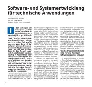
Figure 1: Concept of <strong>the</strong> Method supported by Comos ®
3.2 Tool<br />
To allow <strong>the</strong> advantages of a methodology to pay off in<br />
industrial application, its implementation in software is<br />
mandatory. To achieve <strong>the</strong> user's acceptance,<br />
extraordinary improvements over conventional tools have<br />
to be realized. The main goals during <strong>the</strong> project<br />
described in this paper were<br />
• to guarantee data consistency,<br />
• to automatically generate key documents, and<br />
• to include <strong>the</strong> predevelopment phase in a tool used<br />
for detail engineering.<br />
4. APPROACH<br />
Based on <strong>the</strong> requirements explained in chapter 3, a<br />
method and a tool supporting it, have been developed.<br />
4.1 Method<br />
Figure 2 shows steps to be taken during <strong>the</strong> pre-design<br />
phase (also see 3.1), as suggested in [5]. It is divided into<br />
<strong>the</strong> functional description of a machine and its<br />
infrastructure planning as described below.<br />
Functional Description<br />
A machine is structured according to functional aspects as<br />
recommended in [9]. For every function, an operational<br />
principle (figure 3) and a sequence as a project network<br />
[10] are drawn. Each step in this project network is<br />
assigned to a degree of freedom. For every degree of<br />
freedom a state graph including all attainable states is<br />
defined (also see [4], [11]). Temporary and final states<br />
can be distinguished. While final states are determined by<br />
constant energy within <strong>the</strong> system of interest, temporary<br />
states are required to change from one final state to<br />
ano<strong>the</strong>r. For every transition from a temporary to a final<br />
state, <strong>the</strong> amount of energy within <strong>the</strong> system has to be<br />
determined. Therefore, required measurement quantities<br />
for every degree of freedom can be derived. One example<br />
of a state graph for rising and lowering <strong>the</strong> upper die is<br />
given in figure 4.<br />
Figure 2: Engineering as Supported in Comos ® ME<br />
Figure 3: Operating Principle for a Press<br />
3<br />
Infrastructure Planning<br />
Figure 4: Simple State Graph<br />
After <strong>the</strong> functional description is completed, <strong>the</strong> concepts<br />
defined in operation principles, network diagrams and<br />
state graphs have to be realized with hard- and software<br />
components. Therefore, each degree of freedom is<br />
assigned to an actuator and for every measurement<br />
quantity a sensor is chosen. As suggested in [8], setting<br />
elements – for example valves or relays – elements are<br />
added as required to every degree of freedom. Figure 5<br />
illustrates that <strong>the</strong>n <strong>the</strong> electrical input and output signals<br />
in <strong>the</strong> machine field are determined. Therefore, <strong>the</strong><br />
signals for <strong>the</strong> CNC cabinet can be obtained (also see<br />
figure 6).<br />
Figure 5: Actuators, Sensors and Setting Elements<br />
Figure 6: Connections for Field and Control Components
Derived Documents<br />
As shown in [12], sequential function charts according to<br />
[13] can be received from state graphs and network<br />
diagrams. This kind of document contains a considerable<br />
amount of valuable information for <strong>the</strong> electrical and fluid<br />
design of a machine tool. However, as it does not support<br />
<strong>the</strong> mechanical engineering process, it is rarely provided.<br />
Therefore, a method of automatically generating<br />
functional charts improves <strong>the</strong> interdisciplinary<br />
communication.<br />
Fur<strong>the</strong>rmore, I/O lists can be easily created from<br />
connection diagrams as shown in figure 6 (also see [12]).<br />
4.2 Tool<br />
The documents and data object described in section 4.1<br />
have been integrated into <strong>the</strong> software platform Comos®<br />
[5], a product, which is commonly used in chemical<br />
engineering, which is – like mechatronic engineering –<br />
highly interdisciplinary.<br />
Macros have been provided to perform <strong>the</strong> tasks of<br />
automatically generating key documents, such as<br />
sequential function charts or I/O-Lists. The architecture of<br />
Comos ® is illustrated in figure 7. The component object<br />
server provides an interface between a database, which<br />
saves all project information, and every single engineering<br />
application. Since every piece of information is stored<br />
once in <strong>the</strong> database and depending views link to one<br />
unique record, data consistency is ensured.<br />
The engineering applications "Basic Logical Diagram"<br />
developed by <strong>the</strong> iwb and "Electrical & Instrumentation"<br />
as well as "Hydraulics & Pneumatics" from innotec have<br />
been combined to <strong>the</strong> Comos ® ME bundle.<br />
Figure 7: Architecture of <strong>the</strong> Comos ® Product Family<br />
4<br />
5. CASE STUDY<br />
To prove <strong>the</strong> feasibility of <strong>the</strong> method and tool portrayed in<br />
chapter 4, a complete milling machine has been mapped<br />
in Comos ® in cooperation with an international vendor for<br />
machine tools [14]. All actuators and sensors totaling to<br />
roughly 350 I/O-signals have been modeled in an Access ®<br />
database. Figure 8 shows <strong>the</strong> machine and a screenshot<br />
of a document describing parts <strong>the</strong> electrical wiring.<br />
Information about actuators, sensors and cables have has<br />
been exported to Pro/Engineer via an XML interface<br />
considered in [12] (figure 9). Fur<strong>the</strong>rmore, raw concepts<br />
for <strong>the</strong> PLC software have been generated from <strong>the</strong><br />
sequential function charts and imported into Simatic<br />
Manager in an IEC 61131 format (figure 10).<br />
Figure 8: Electrical Connections of a Machine in Comos ®<br />
Figure 9: Interface to 3D-CAD-System<br />
Figure 10: Interface to PLC-Environment
6. CONCLUSIONS AND FUTURE WORK<br />
The development of <strong>the</strong> Comos ® ME system is an<br />
example, how <strong>the</strong> cooperation between a university and a<br />
software vendor can lead to innovative and promising<br />
products. The research work completed by <strong>the</strong> iwb and<br />
<strong>the</strong> software framework from innotec GmbH lead to a new<br />
generation of engineering tools, ready to enter <strong>the</strong> market.<br />
The viability <strong>the</strong> method and <strong>the</strong> toll described in chapter<br />
4 has been proven in a case study sketched in chapter 5.<br />
Fur<strong>the</strong>r work will focus on customizing <strong>the</strong> COMOS ® ME<br />
to <strong>the</strong> requirements of users. The integration of <strong>the</strong><br />
engineering environment and certain simulation tools, for<br />
example hardware-in-<strong>the</strong>-loop systems as described in<br />
[15] and [16], may lead to even more improved<br />
development cycles in <strong>the</strong> field of mechatronic<br />
engineering.<br />
[1] Harashima, F.; Tomizuka, M.; Fukuda, T.; 1996:<br />
Mechatronics – What Is It, Why, and How? – An<br />
Editorial, IEEE/ASME Transactions on Mechatronics,<br />
Vol. 1, No. 1, 1996, pp. 1-4<br />
[2] Reinhart, G.; Egermeier, H.; Thieke, S.; Dürrschmidt,<br />
S.; 2001: Mechatronik, In: offprint of Enzyklopädie<br />
Naturwissenschaft und Technik, addendum 7<br />
[3] VDI 2221, 1993: Methodik zum Entwickeln und<br />
Konstruieren technischer Systeme und Produkte.<br />
[4] VDI/VDE 2422; 2001: Entwicklungsmethodik für<br />
Geräte mit Steuerung durch Mikroelektronik.<br />
[5] Zaeh, M. F.; Graetz, F.; Rashidy, H., 2003: An<br />
Approach to Simultaneous Development in Machine<br />
Tool industry, Proceedings on International<br />
Workshop on Modeling and Applied Simulation, pp.<br />
128-133, Bergeggi, Italy.<br />
[6] VDI 2206, 2004: Design Methodology for<br />
Mechatronic <strong>Systems</strong>.<br />
[7] Zaeh, M. F.; Graetz, F.; Rashidy, H., 2004:<br />
Installation Planning for Mechatronic Production<br />
<strong>Systems</strong>, Proceedings on <strong>the</strong> IEEE-Conference<br />
"Mechatronics & Robotics 2004", pp. 315-319,<br />
Aachen, Germany.<br />
[8] Zaeh, M. F.; Graetz, F.; Gerdelmann, U.; 2003: Neue<br />
Konstruktion – Mechatronische Systeme Systeme<br />
erfordern neue Konstruktionswerkzeuge, SPS-<br />
Magazin, vol. 11//2003, pp. 68-70.<br />
[9] VDI 2800, 2000: Value Analysis.<br />
[10] DIN 69900-2, 1987: Project Controlling, Project<br />
Network Techniques, Methods of Presentation.<br />
[11] PG3, 2001: Projektgruppe 3, Richtlinie<br />
Funktionsbeschreibung.<br />
[12] Zaeh, M. F.; Graetz, F.; Rashidy, H., 2004:<br />
Installationsplanung – Entwicklung von<br />
mechatronischen Produktionssystemen. In:<br />
Konstruktion 7/8-2004, pp. 59-62.<br />
[13] IEC 60848, 2002: GRAFCET specification language<br />
for sequentional function charts.<br />
[14] Zaeh, M. F.; Graetz, F.; Rashidy, H., 2004: A<br />
Platform for Installation Planning – a case study. In:<br />
Proceedings of <strong>the</strong> CIRP Design Seminar 2004,<br />
Cairo, Egypt.<br />
[15] Maier, M.; Dierssen, S.; Ba<strong>the</strong>lt, J., 2004: Die<br />
Virtuelle Maschine – oder wie Inbetriebnahme vor<br />
Montage möglich ist. In: Seminarband zum<br />
Chemnitzer Produktionstechnischen Kolloquium<br />
2004, pp. 365-380.<br />
5<br />
[16] Zaeh, M. F.; Poernbacher, C.; Wuensch, G., 2003:<br />
Emerging Virtual Machine Tools. In: Proceedings of<br />
<strong>the</strong> DETC 2003, 29 th Design Automation<br />
Conference, Chicago, Illinois.
vibration-based interface as one sort of <strong>the</strong> forcefeedback<br />
one.<br />
Figure 6: System configuration of vibration-based<br />
interface.<br />
Figure 6 shows a configuration of vibration-based<br />
interface developed in this reseach. 4 sets of vibration<br />
motor are used to give a vibration siglal to <strong>the</strong> user. The<br />
vibration motors are controlled by PIC microchip on a<br />
control circuit, based on <strong>the</strong> signals transmitted from PC<br />
through RS-232C serial line. This interface is used by<br />
hand movement of a user, of which position in 3D space<br />
is traced by a magnetic sensor system composed of a<br />
controller, transmitter, and receiver.<br />
Figure 7: User interaction with vibration-based interface.<br />
Figure 7 shows a user interaction with a virtual object via<br />
this vibration-based interface. The user wearing a glove<br />
and a headband in Figure 7 is under manipulation on <strong>the</strong><br />
object in <strong>the</strong> screen. The glove is equipped with magnetic<br />
sensor to trace <strong>the</strong> position and orientation of hand to<br />
manipulate <strong>the</strong> object which is shown in <strong>the</strong> computer<br />
screen. The headband is equpped with 4 vibration motors,<br />
which start and/or stop vibration in various strength<br />
corresponding to <strong>the</strong> signals to feed back to <strong>the</strong> user.<br />
When <strong>the</strong> user touches <strong>the</strong> object, <strong>the</strong> system returns a<br />
signal so that <strong>the</strong> user can feel that his hand touches <strong>the</strong><br />
object. The vibration interface is equipped with 4 vibration<br />
motors. With <strong>the</strong> combination of <strong>the</strong>se 4 motors, <strong>the</strong><br />
system provides <strong>the</strong> direction toward which <strong>the</strong> user<br />
touches <strong>the</strong> object as well. If <strong>the</strong> user touches from <strong>the</strong> 45<br />
degree to <strong>the</strong> object front, vibration motor 2 and 3 are on<br />
in <strong>the</strong> same strength of vibration, whereas, for example,<br />
<strong>the</strong> user touches <strong>the</strong> object from 60 degree to <strong>the</strong> object<br />
front, or more horizontal direction, vibration of motor 3 is<br />
stronger than that of 2. If <strong>the</strong> user touches around <strong>the</strong><br />
object, <strong>the</strong> vibration moves around <strong>the</strong> object according to<br />
<strong>the</strong> touching point, so that <strong>the</strong> user can feel from which<br />
direction <strong>the</strong> user is currently touching <strong>the</strong> object as a real<br />
time interaction.<br />
Figure 8: Vibration mechanism in remote object<br />
manipulation.<br />
Figure 8 shows a series of interaction with virtual object<br />
with virtual hand which is controlled by <strong>the</strong> user’s hand<br />
through <strong>the</strong> vibration-based interface. When <strong>the</strong> hand is<br />
away from <strong>the</strong> object as show in Picture 1 in Figure 8, no<br />
vibration is given to <strong>the</strong> user. The user moves around <strong>the</strong><br />
hand and it touches to <strong>the</strong> object from <strong>the</strong> front direction<br />
as shonw in Picture 2, vibration starts on motor #2 on <strong>the</strong><br />
front position. During <strong>the</strong> move of object by pushing with<br />
hand, vibration becomes stronger so that <strong>the</strong> user has a<br />
feeling of pushing <strong>the</strong> object. The user keeps on pushing<br />
<strong>the</strong> object along <strong>the</strong> crank-shape route, changing <strong>the</strong><br />
direction of pushing from front-foward to right-forward,<br />
<strong>the</strong>n front-forward direction, during which <strong>the</strong> vibration site<br />
changes corresponding to <strong>the</strong> move so that <strong>the</strong> user also<br />
9
has a feeling of pushing to each direction to follow <strong>the</strong><br />
route to reach <strong>the</strong> goal. The pictures on <strong>the</strong> right hand<br />
side in Figure 8 shows how <strong>the</strong> vibration position changes<br />
during this operation.<br />
Figure 9: Snapshot of computer screen for vibrationbased<br />
interface.<br />
This vibration-based interface not only provides a control<br />
function with digital objects but also provides an interface<br />
to control a mechatronics object. For example, Figure 9<br />
shows a snapshot of teleoperation interaction to <strong>the</strong><br />
remote object. The user in <strong>the</strong> local site is under video<br />
conference with a remote site, where a cylinder-shaped<br />
object can be recognized through video Window 1 on <strong>the</strong><br />
left side of <strong>the</strong> screen. What <strong>the</strong> local user is doing is to<br />
move <strong>the</strong> object with his hand. The object is equipped<br />
with 2 DC motors so that it can be controlled to move in<br />
any direction if a control signal is given to it. A hand in<br />
Window 2 on <strong>the</strong> right side of <strong>the</strong> cylinder-shaped object<br />
is a virtual hand which is corresponding to <strong>the</strong> real hand of<br />
<strong>the</strong> manipulating person in terms of movement of hand.<br />
The user can feel <strong>the</strong> touching point on <strong>the</strong> object, and<br />
also feel <strong>the</strong> vibration indicating <strong>the</strong> direction to which <strong>the</strong><br />
user should move it. It also means that <strong>the</strong> user can move<br />
<strong>the</strong> object to <strong>the</strong> appropriate direction even if <strong>the</strong> user<br />
cannot see <strong>the</strong> window, because <strong>the</strong> vibration signal gives<br />
<strong>the</strong> direction to him. The participants in <strong>the</strong> video<br />
conference can manipulate <strong>the</strong> object with a touch and<br />
feel of movement, which actually controls <strong>the</strong> real object.<br />
3.2 Force-feedback lever interface for mechatronics<br />
design review<br />
Physical interaction plays a very important role in design<br />
review of mechatronics products, for example, a<br />
mechatronics devive. Designers study not only <strong>the</strong><br />
appearance of <strong>the</strong> device but also embedded function and<br />
usability of it. Designers touch <strong>the</strong> device, use it and<br />
check <strong>the</strong> function to discusses <strong>the</strong> feasibility of <strong>the</strong><br />
design. Design review could also be carried out in a video<br />
conference system over <strong>the</strong> network so that participants<br />
remotely distributed should join <strong>the</strong> discussion. However,<br />
physical interaction with <strong>the</strong> device is not available in a<br />
conventional video conference system, including<br />
CELAVIS. This research pays attention on <strong>the</strong> idea of<br />
physical interaction in video conference system, for<br />
example, <strong>the</strong> usage of vibration-based interface as<br />
described in <strong>the</strong> previous section. This section describes<br />
a senario of physical interaction for design review of a<br />
mechatronics device.<br />
Figure 10 shows a force-feedback controller which is<br />
under development as a part of this research. The lever<br />
on <strong>the</strong> right side of <strong>the</strong> box is designed to control <strong>the</strong> up-<br />
10<br />
down movement of a target device. A DC motor in <strong>the</strong> box<br />
generates a dynamic torque based on <strong>the</strong> angle of<br />
movement detected by potentiometers. The lever returns<br />
a force-feedback to a user so that it can be used as an<br />
interface for object manipulation.<br />
Figure 10: A controller with a force-feedback lever.<br />
Figure 11 shows a snapshot of computer screen during<br />
video conference to have design review on some devices<br />
in dental applications. Window 1 in Figure 11 shows a<br />
physical measurement device, called micro-surveyor,<br />
which is used to examine abutment teeth, design dentures,<br />
and to make parallel measurements of abutment teeth for<br />
bridges in dental applications. The window shows a<br />
measurement to check <strong>the</strong> jaw bone condition using a<br />
physical jaw bone model. The pen of <strong>the</strong> micro-surveyor<br />
has free movement on x-y horizontal surface, and updown<br />
movement on its vertical axis.<br />
Window 2 in Figure 11 shows a digital prototype which is<br />
identical to <strong>the</strong> micro-surveyor and jaw bone in Window 1.<br />
We have implemented manipulation software so that this<br />
digital compass can be manipulated by a controller such<br />
as joystick. A user can move up-and-down <strong>the</strong> pen to<br />
check <strong>the</strong> jaw condition, however, <strong>the</strong> user cannot have a<br />
feeling of touching to <strong>the</strong> jaw bone even if <strong>the</strong> pen touches<br />
it or penetrate to inside of <strong>the</strong> jaw bone. We have adopted<br />
<strong>the</strong> force-feedback lever controller shown in Figure 10 to<br />
manipulate <strong>the</strong> movement of <strong>the</strong> pen. In combination with<br />
ano<strong>the</strong>r controller under development, <strong>the</strong> user can<br />
control <strong>the</strong> movement of a virtual micro-surveyor in a<br />
touch and feeling manner, which could control an actual<br />
mechatronics micro-surveyor if it is designed to be<br />
controllable by PC.<br />
Figure 11: Snapshot of computer screen of interactive<br />
manipulation in video conference.
4. Concluding remarks<br />
A number of commercial or free systems are available, as<br />
<strong>the</strong> increasing demand on video conference for business,<br />
technical, and routine meetings. The main objective of<br />
<strong>the</strong>se systems is to provide an environment for<br />
audio/video communication for participants. If we need to<br />
have a video phone conversation with <strong>the</strong> counterparts,<br />
<strong>the</strong>n it surely works fine. We have developed CALAVIS<br />
system as we described in this paper, and we have<br />
confirmed that our small group meeting which we held a<br />
couple of times between Japan and US sites works quite<br />
fine.<br />
In our video meeting experiments, we also have found<br />
that when we have a face-to-face meeting, what we would<br />
like to share is not only <strong>the</strong> information which is discussed<br />
in <strong>the</strong> conference but also <strong>the</strong> data, software, or physical<br />
devices on which <strong>the</strong> agenda of meeting might be related.<br />
Currently available system including CALAVIS does not<br />
provide such an environment where participants can<br />
share those items. What we are pursuing as one of <strong>the</strong><br />
objectives in this study is to setup an environment where<br />
participants can share a virtual workspace where <strong>the</strong>y can<br />
work with <strong>the</strong> common sharing of those items as well as<br />
have a video conference.<br />
This study focuses on <strong>the</strong> physical aspects of interaction<br />
in video conference, which means that participants not<br />
only should share information/data through visual<br />
interactions but also should share <strong>the</strong>m through physical<br />
interactions to work toge<strong>the</strong>r much more collaboratively.<br />
For this objective, this paper presented a web-based<br />
video conference system with vibration-based interface to<br />
manipulate a remote mechatronics object through virtual<br />
space. Our system makes it possible to have physical<br />
interaction with <strong>the</strong> object over <strong>the</strong> network.<br />
The vibration-based interface presented in this paper is<br />
not as powerful as forced-feed back device interaction but<br />
users can feel <strong>the</strong> manipulation. While vibration signal is<br />
commonly used to draw attention from users, such as<br />
silent mode of mobile phone, and to let <strong>the</strong>m know<br />
something, such as phone call, or new messages, etc.,<br />
but it is not suitable to guide physical direction to users to<br />
support manipulation. With <strong>the</strong> combination of multiple<br />
vibration motor based on a simple protocol to show<br />
direction of movement, <strong>the</strong> interface of our system<br />
provides not only signals of notice, but also guidance of<br />
manipulation. For example, a user may receive vibration<br />
signal at <strong>the</strong> time of contact with an object during<br />
manipulation, and <strong>the</strong>n may be given directional vibration<br />
to move accordingly. Reporting <strong>the</strong> result of experiment<br />
using a simple mechatronics prototype via vibration-based<br />
interface for collaboration, <strong>the</strong> paper discussed <strong>the</strong><br />
feasibility of <strong>the</strong> interface for collaboration as well as <strong>the</strong><br />
usability of <strong>the</strong> interface.<br />
BOCOLLA interface presented in this paper is also a new<br />
approach to support collaborative work over video<br />
conference. When we have a meeting, we often use a<br />
whiteboard-like panel to write down words, phrases,<br />
figures, marks, etc., which surely support understanding<br />
each o<strong>the</strong>r with reducing difficulty and mistakes caused by<br />
miscommunication, and with increasing easiness and<br />
mutual understanding supported by visual aides. With<br />
only a marker pen, participants can not only control<br />
computers located locally or remotely, but also even<br />
manipulate teleoperation to control a remote machine<br />
located on a remote site. Although what we did in this<br />
study was limited to a simple operation on a miniature<br />
crane, but we are actually able to manipulate various<br />
kinds of devices, including remote computers, mechanical<br />
machines, electrical devices, home appliances, etc. only if<br />
we can make it available to control <strong>the</strong>m via IT network,<br />
which can be available in a variety of ways.<br />
What we have employed in our test environment was a<br />
teleoperation as an example of collaborative work during<br />
video conference. To do so, we have prepared a toy<br />
crane and controller, both of which can be connected to<br />
PC ei<strong>the</strong>r locally or remotely, so that an operator can<br />
control it during video conference. BOCOLLA interface<br />
allows participants to control <strong>the</strong> crane during <strong>the</strong><br />
conference. Vibration-based interface presented in this<br />
paper can also be used as an interface. Participants can<br />
have a touch-and-feel of control on <strong>the</strong> crane. The forcefeedback<br />
lever presented in this paper can also be<br />
integrated in this test environment to support physical<br />
interaction in video conference.<br />
The idea of physical interaction presented in this paper is<br />
to support much more collaboration in mechatronics<br />
design over <strong>the</strong> network. We will continue our research,<br />
and work much more on <strong>the</strong> development on each<br />
interface modules and subsystems to implement an<br />
integrated test environment. Using such an integrated<br />
environment, we will study <strong>the</strong> feasibility of our idea in<br />
more practical scenarios.<br />
11<br />
Acknowledgement<br />
This research was supported in part by <strong>the</strong> Grants-in-Aid<br />
for Scientific Research in 2003-2004 (Scientific Research<br />
(C) 15500347) from <strong>the</strong> Japan Society of Promotion of<br />
Science. The author would like to thank Prof. Teisuke<br />
Sato of Department of Mechanical Engineering, and Prof.<br />
Tetsuo Ichikawa, Dr. Yoritoki Tomotake, DDS. Keiko<br />
Shibutani of School of Dentistry of <strong>the</strong> University of<br />
Tokushima, Prof.Koichi Sairyo of School of Medicine at<br />
<strong>the</strong> University of Tokushima, Dr. Andrew Milne of Stanford<br />
University. The author would also like to thank <strong>the</strong><br />
members of Collaborative Engineering <strong>Laboratory</strong> at <strong>the</strong><br />
University of Tokushima.<br />
References<br />
[1] Ito, T. 2004, Vibration-based interface for remote<br />
object manipulation in video conference system, 13 th<br />
IEEE International Workshop on Robot and Human<br />
Interactive Communication, Kurashiki, Japan, pp.295-<br />
300.<br />
[2] Ito, T. 2004. (ed. K. Chen, D.Webb and R. March), An<br />
approach of virtual environment for planning of implant<br />
placement, Advances in e-Engineering and Digital<br />
Enterprise Technology. Pp.355-362.<br />
[1] Johanson, B., A. Fox, T Winograd. 2002. “The<br />
Interactive Workspaces Project: Experiences with<br />
Ubiquitous Computing Rooms.” IEEE Pervasive<br />
Computing Magazine April-June, 1/2:71-78.<br />
[2] Milne, A., T. Winograd. 2003. “The iLoft Project: A<br />
Technologically Advanced Collaborative Design<br />
Workspace as Research Instrument.” Proc. Int’l Conf.<br />
on Engineering Design ICDE2003, Stockholm, August,<br />
pp-no.1657.<br />
[3] Ponnekanti, S. R., B. Johanson, E. Kiciman and A. Fox.<br />
2003. “Portability, Extensibility and Robustness in<br />
iROS.” Proc. IEEE International Conference on<br />
Pervasive Computing and Communications<br />
(Percom2003), Dallas-Fort Worth, TX. March.<br />
[4] Telemedical.com home page URL<br />
http://www.telemedical.com/Telemedical/Products/vidc<br />
onf.htm
XML-based Product and Process Data Representation for Distributed Process Planning<br />
Dušan N. Šormaz, Jaikumar Arumugam, Narender Neerukonda<br />
Department of Industrial and Manufacturing <strong>Systems</strong> Engineering<br />
Ohio University, A<strong>the</strong>ns, OH 45701<br />
Abstract<br />
The need to exchange product and process data between different software applications has been identified<br />
across manufacturing industries. An efficient model for communications between CAD, CAPP and CAM<br />
applications in distributed manufacturing planning environment has been seen as key ingredient for CIM.<br />
The paper proposes neutral, XML-based representation for product data required for process planning and<br />
for process data required for downstream manufacturing applications (like cell design, and scheduling). The<br />
representation is based on established standards for product data exchange and serves as a prototype<br />
implementation of <strong>the</strong>se standards. The procedures for writing and parsing XML representations have been<br />
developed in object-oriented approach, in such a way that each object from object oriented model is<br />
responsible for storing its data into XML format. Similar approach is adopted for reading and parsing of <strong>the</strong><br />
XML model. Parsing is preformed by a stack of XML handlers, each corresponding to a particular object in<br />
XML hierarchical model. This is very useful approach for direct distributed applications, in which data are<br />
passed in <strong>the</strong> form of XML streams to allow on-line communication. The components of <strong>the</strong> XML model for<br />
product and process data are explained in <strong>the</strong> paper, <strong>the</strong> mechanism and procedures for writing and parsing<br />
<strong>the</strong> XML model are described. The feasibility of <strong>the</strong> proposed model is verified in a sample scenario for<br />
distributed manufacturing planning that involves feature mapping from CAD file, process selection for<br />
several part designs and selection of alternative processes using scheduling criteria.<br />
Keywords:<br />
1 INTRODUCTION<br />
Computer Integrated Manufacturing (CIM) is still moving<br />
target in industrial and manufacturing engineering<br />
research and applications. There are numerous reports<br />
outlining individual islands of automation within <strong>the</strong> CIM<br />
model, with a significant effort in research papers being<br />
focused on a particular task, and much less effort devoted<br />
to integration of <strong>the</strong>se manufacturing engineering and<br />
planning tasks. Integration involves <strong>the</strong> transfer of data<br />
between applications, but also should focus on data and<br />
model integrity, distributed processing of <strong>the</strong> data,<br />
incorporation of knowledge into <strong>the</strong> planning tasks, and so<br />
on. Computer aided process planning (CAPP) is rightly<br />
seen as an integration fabric for CIM with its relations to<br />
design (CAD), manufacturing (CAM), and scheduling<br />
tasks. By virtue of being an integrator between CAD,<br />
CAM, and scheduling, process planning involves decision<br />
making process on various levels of details with <strong>the</strong> final<br />
goal of generating feasible and/or optimal process plan.<br />
The need for integration requires that such model is<br />
transparent between <strong>the</strong>se tasks, that it can be easily<br />
saved, transferred, and re-created as needs arise.<br />
This paper proposes such neutral data model in <strong>the</strong> form<br />
of XML model and describes its details and application in<br />
manufacturing process planning. The paper is organized<br />
as follows. Section 2 describes previous work in process<br />
plan representation and modeling. Section 3 describes<br />
process planning representation object model, which<br />
includes major entities and relations between <strong>the</strong>m.<br />
Section 4 explains process planning XML schema model<br />
that is built for previous object model. Section 5 describes<br />
a flexible mechanism for writing data in XML format and<br />
parsing XML streams into object model. Section 6<br />
describes a sample scenario of integration between<br />
process selection and scheduling using data in XML<br />
format. The paper ends with conclusions and <strong>the</strong> list of<br />
references.<br />
12<br />
2 PREVIOUS WORK<br />
Data and knowledge representation in process planning<br />
have received significant interest in research. An early<br />
work on ALPS [1] proposed a graphical representation for<br />
manufacturing processes and means for specifying serial,<br />
parallel and concurrent tasks. Since <strong>the</strong>n, several papers<br />
addressed knowledge representation, for example, using<br />
frames and rules [2] or an object-oriented data model [2].<br />
International standard for product data exchange (STEP)<br />
has been developed to enable data transfer between<br />
applications that includes process data [8]. Recent results<br />
are in generation of <strong>the</strong> Process Specification Language<br />
(PSL) as a neutral format for <strong>the</strong> specification of process<br />
representation and exchange of different ontologies or<br />
semantics between various domains. Development of<br />
process planning specific, NC data within STEP standard<br />
has been described in [3]. Work on XML [6], as a very<br />
flexible language that transfers both data and <strong>the</strong>ir<br />
description (metadata) prompted its widespread use in<br />
many research efforts. Paper [12] discusses similarities<br />
and differences between STEP and XML and proposes<br />
<strong>the</strong>ir convergence.<br />
3 PROCESS PLANNING REPRESENTATION AND<br />
MODELING<br />
Manufacturing planning object model developed in this<br />
work is based on process planning object model proposed<br />
in [2], which described a data model for representation of<br />
process plans based on <strong>the</strong> different activities involved in<br />
manufacturing. A process planning representation model<br />
facilitates <strong>the</strong> development of algorithms for<br />
manufacturing problems like sequencing, scheduling etc.<br />
by reducing <strong>the</strong> over-all algorithm development time. The<br />
model accommodates a variety of data that may be<br />
needed in manufacturing planning algorithms.<br />
Components of <strong>the</strong> model are manufacturing planning<br />
model, feature object model, and process object model<br />
and <strong>the</strong>y are described in this section.
3.1 Manufacturing planning object model<br />
Manufacturing planning object model is shown in Figure 1.<br />
The model is based on analysis of product and process<br />
design entities and includes hierarchical representation of<br />
manufacturing activities, that has manufacturing<br />
processes as its leaves, collection of manufacturing<br />
features and corresponding manufacturing processes,<br />
and a collection of machines used in <strong>the</strong> manufacturing<br />
system.<br />
A manufacturing activity represents <strong>the</strong> core of <strong>the</strong> model.<br />
Any activity that contributes to <strong>the</strong> manufacturing of a part<br />
is called as a manufacturing activity. A manufacturing<br />
activity has attributes like manufacturing cost,<br />
manufacturing time, member process etc. A<br />
manufacturing activity is subdivided as a part activity, a<br />
machine activity or a tool direction activity. A part activity<br />
describes <strong>the</strong> process plan for a part. There is an<br />
association relationship between part activity and part.<br />
Each part activity is associated with a part. A process plan<br />
for a part is a collection of <strong>the</strong> machines through which a<br />
part has to pass through to be completely manufactured.<br />
The part in turn can have multiple alternative process<br />
plans. The machining process of a part on each machine<br />
in its process plan is represented by a machine activity.<br />
Each machine activity is associated with a machine<br />
object. There is an aggregation relationship between part<br />
activity and machine activity. Each part activity is a<br />
collection of machine activities. The part object has<br />
attributes like a collection of its alternative process plans,<br />
part material, features list, process list etc. The machine<br />
object has attributes like machine name, number of units,<br />
usage frequency, SICGE code etc. Each machine activity<br />
is a collection of tool direction activities. A tool direction<br />
activity holds directional information about a machining<br />
process. The member process attribute of manufacturing<br />
activity is used to store <strong>the</strong> aggregations of a<br />
manufacturing activity. Thus, <strong>the</strong> member process<br />
attribute of a part activity holds a collection of machine<br />
activity. The member process attribute of a machine<br />
activity holds a collection of tool direction activities. The<br />
representation model for <strong>the</strong> cellular manufacturing shown<br />
in Figure 2 is built on <strong>the</strong> basis of <strong>the</strong> process plan<br />
Figure 1.Process plan representation model for manufacturing<br />
representation model and serves as its extension for cell<br />
formation.<br />
Figure 2. Cellular manufacturing representation model<br />
The core of <strong>the</strong> cellular manufacturing model is <strong>the</strong><br />
manufacturing system. A manufacturing system is a place<br />
where parts are manufactured on machines. The main<br />
task of cell formation is <strong>the</strong> partition of <strong>the</strong> parts in <strong>the</strong><br />
system into part families and machines into machine cells<br />
to reduce intercellular traffic. The objective is to find a<br />
partition for machines into machine cells and parts into<br />
part families in such a way as to minimize intercellular<br />
traffic.<br />
3.2 Feature object model<br />
Feature object model represents a hierarchical<br />
representation of various machining features with<br />
inheritance relations within it. The model is shown in<br />
Figure 3. The major class is MfgFeature that abstracts all<br />
common properties for all features. Properties at this level<br />
include feature name, containing part, tolerance data, list<br />
of alternative processes, and precedence relations.<br />
MfgFeature class is extended into several subclasses that<br />
correspond to machining feature types found in<br />
mechanical prismatic parts (such as Hole, Slot, and<br />
Pocket). These classes model properties of particular<br />
feature type and include different dimension parameters,<br />
and process capability data. However, model properties<br />
on general, feature ,level are of generic nature and can be<br />
applied by extending this model to o<strong>the</strong>r domains (like<br />
rotational parts, sheet metal parts, and so on). Model also<br />
contains several auxiliary classes that serve <strong>the</strong> purpose<br />
of generating various feature relations and displaying<br />
<strong>the</strong>m to user.<br />
13
javax.swing.filechooser.FileFilt<br />
SaveFilter<br />
Exception<br />
UnsupportedFeatureExcept<br />
TableCellGenerator<br />
mfgFeatureInteractorGenerat<br />
TestPocket<br />
java.awt.event.ActionListen<br />
...actionAdapter<br />
Pocket<br />
Hole<br />
+HolePanel<br />
3.3 Machining process object model<br />
The knowledge about processes is also represented in an<br />
objected-oriented model. In order to map this knowledge<br />
representation, <strong>the</strong> machining processes are categorized<br />
based on <strong>the</strong>ir characteristics. Figure 4 presents this<br />
hierarchy in a UML based model.<br />
The class MfgProcess represents <strong>the</strong> most generic<br />
process class, i.e., a process with <strong>the</strong> common data<br />
shared by <strong>the</strong> rest of <strong>the</strong> processes. Fur<strong>the</strong>r distinctions<br />
are carried out based on <strong>the</strong> process characteristics such<br />
as hole making processes and profile generating milling<br />
processes. The hole making processes are fur<strong>the</strong>r divided<br />
into CoreMaking, HoleStarting and HoleImproving<br />
processes, while <strong>the</strong> Milling process has as sub-type<br />
java.awt.event.ActionListen<br />
...actionAdapter MfgPartMode<br />
TableCellGenerator<br />
MyMfgPartModel<br />
mfgFeatureNeighborGenera<br />
ImpObject<br />
MfgFeature<br />
MfgFeatureContentHandle<br />
ImpXmlHandler<br />
MfgFeatureSubclassHand<br />
Figure 3. Class diagram for features<br />
TableCellGenerator<br />
MfgFeaturePrecedenceGenera<br />
Slot<br />
+SlotPanel<br />
Figure 4. Machining process hierarchy<br />
14<br />
FeatureSet<br />
javax.swing.filechooser.FileFilt<br />
PartFilter<br />
InstanceFeature<br />
CheckBoxListene<br />
DovetailSlot TSlot<br />
LinearFeatureSe CircularFeatureSe<br />
EndMilling process. These generalized classes are<br />
implemented as abstract classes and are shown with<br />
italicized titles in Figure 4. The classes under <strong>the</strong>se<br />
umbrella classes are for representing <strong>the</strong> actual<br />
machining processes (for example, TwistDrilling,<br />
EndMIllingSlotting, or FaceMilling). Therefore, based on<br />
<strong>the</strong> inheritance, EndMillingSlotting process acquires<br />
process information from ‘Endmilling’, which fur<strong>the</strong>r leads<br />
to <strong>the</strong> parent class MfgProcess’. The following<br />
paragrpahs give a brief description about <strong>the</strong> MfgProcess<br />
and EndMilling classes., while description of o<strong>the</strong>r classes<br />
is part of working documentation.<br />
MfgProcess: This class contains member variables such<br />
as feature, stock, workpiece, cutting parameters,
constraints, tool, and tool path. These listed variables are<br />
used in every inherited process class as every process<br />
contains <strong>the</strong>se components of machining process. Also,<br />
this class carries <strong>the</strong> GUI components for showing<br />
process information and a graphical interface to display a<br />
process.<br />
EndMilling: The implementation for visualization is mainly<br />
concentrated on end milling operations, so this class<br />
contains some graphical components. This class provides<br />
methods to prepare <strong>the</strong> scene graph, which carries nodes<br />
to display machining process components and <strong>the</strong><br />
animation for visualization. The GUI required for eventbased<br />
interaction with <strong>the</strong> virtual world displayed is<br />
provided in this class. The subclasses --slotting and<br />
peripheral end milling-- use this implementation with<br />
distinctive modifications in tool approach for machining.<br />
4 PROCESS PLANNING XML SCHEMA MODEL<br />
This section discusses <strong>the</strong> persistent and neutral data<br />
storage mechanism for <strong>the</strong> process plan representation<br />
model (PPRM) based on XML. It describes <strong>the</strong> XML<br />
schema which is <strong>the</strong> basis or template for process plan<br />
data generation, and provides few examples of XML data.<br />
A schema is a set of rules that have to be satisfied in valid<br />
XML document [6]. Figure 5 shows <strong>the</strong> XML Schema<br />
definition for <strong>the</strong> process plan representation model as<br />
shown in a tool for XML development XMLSpySuite.<br />
Figure 5.XML schema for PPRM from XML Spy Suite.<br />
The root element of <strong>the</strong> schema is that<br />
holds all information about a factory model. This element<br />
holds two collection elements and<br />
. The element is a collection of<br />
part models represented by <strong>the</strong> element.<br />
The is a collection of <strong>the</strong> available<br />
machines represented by element. Each<br />
element has a list element called<br />
, which is a collection of alternative<br />
process plans, for <strong>the</strong> enclosing part element. These<br />
alternative process plans are represented as<br />
elements on <strong>the</strong> part model. Each<br />
element has a <br />
element. The element is a<br />
collection of all <strong>the</strong> elements in <strong>the</strong><br />
enclosing process plan. Each element<br />
encloses a element that holds information<br />
about <strong>the</strong> machine on which <strong>the</strong> machining operation is<br />
done. Each element holds a<br />
element, This element holds<br />
<strong>the</strong> spatial information about <strong>the</strong> tools used in this<br />
machining activity. in turn, holds<br />
element as reference to a machining<br />
process. The hierarchical relationship between parts,<br />
machines, part activities, machine activities, tool activities,<br />
features and processes is in such way incorporated into<br />
<strong>the</strong> XML document.<br />
Information on features and processes may be included in<br />
few levels of detail. For feature modeling, geometric<br />
reasoning and process selection all details are needed, so<br />
element actually carry <strong>the</strong> name of <strong>the</strong> feature or process<br />
class, with inclusion of all details. Example of this model<br />
for two features is shown in Figure 6. Feature tags are<br />
actually class names, and feature have all details of <strong>the</strong>ir<br />
dimensions stored.<br />
Figure 6. Detailed XML data for features<br />
Different XML elements are used when feature and<br />
process data are used in cell formation or scheduling, as<br />
will be shown in detailed example in section 6.<br />
5 MECHANISM FOR WRITING AND PARSING XML<br />
DATA<br />
This section describes flexible mechanism for generation<br />
of XML data from Java and reconstruction of class<br />
instances from XML code.<br />
5.1 XML data generation mechanism<br />
An object-oriented data generation framework was<br />
constructed for <strong>the</strong> purpose of generating XML data for<br />
factory models based on <strong>the</strong> process plan representation<br />
model. The different entities whose XML data needs to be<br />
generated for <strong>the</strong> factory model include MfgPartModel,<br />
Machine, PartActivity, MachineActivity and<br />
ToolDirectionActivity, MfgFeatue and MfgProcess. All <strong>the</strong><br />
Java classes built for <strong>the</strong> process plan representation<br />
model are capable of generating self-describing XML<br />
data. We propose two alternative ways for achieving this<br />
goal: a) each class implements methods for XML data<br />
generation, or b) XML data generation is delegated to<br />
special XML writer classes.<br />
The first approach was used for Machine class as shown<br />
in Figure 7 where <strong>the</strong> code for its method writeXML() is<br />
given. The Machine class holds data about <strong>the</strong> machine<br />
like name, number of units, usage frequency, SICGE code<br />
etc. It is this state data for each machine that needs to be<br />
saved into XML.<br />
15<br />
<br />
<br />
<br />
<br />
<br />
<br />
Figure 7. Machine Java class showing XML data<br />
generation mechanism
To establish uniformity, a method called writeXML() with<br />
<strong>the</strong> following syntax is defined fro each class using this<br />
way:<br />
public void writeXML (StringBuffer xmlTarget,<br />
String indent)<br />
This method is called on <strong>the</strong> Java class whenever data<br />
about <strong>the</strong> state of an instance of <strong>the</strong> class has to be<br />
generated in <strong>the</strong> form of XML. The argument xmlTarget<br />
holds all <strong>the</strong> factory model information generated in XML<br />
form until <strong>the</strong> Machine class method was called. The<br />
generated XML data from <strong>the</strong> Machine class is <strong>the</strong>n<br />
included in <strong>the</strong> xmlTag variable. The indent argument is to<br />
generate properly indented XML code to improve<br />
readability.<br />
Alternative approach is to implement XML writer class for<br />
each PPRM class. The XML writers write out XML data at<br />
a given state of manufacturing process planning .The<br />
PartWriter writes part material and part activities. It calls<br />
FeatureWriter to write <strong>the</strong> feature data.<br />
The feature writers also work in <strong>the</strong> same manner. The<br />
FeatureWriter writes <strong>the</strong> dimensional details like radius,<br />
depth, axis and axis-point about <strong>the</strong> feature. It gives a call<br />
to <strong>the</strong> PropertyTableWriter which writes <strong>the</strong> tolerance<br />
details like surface finish, roundness, true position and<br />
straightness. It also calls ProcessWriter that writes data<br />
fro alternative processes like, class name (type), process<br />
name, cutting parameters, machine name, process time<br />
and cost. This chain of XML data writing is shown in<br />
Figure 8.<br />
Part Writer<br />
Feature Writer<br />
Process Writer<br />
Part name<br />
Part material<br />
Batch size<br />
Call feature writer<br />
Call activity writer<br />
Feature name<br />
Radius<br />
Depth<br />
Axis<br />
Axis point<br />
Call tolerance writer<br />
Call process writer<br />
Tool Material<br />
Depth of cut<br />
Cutting parameters<br />
Machine name<br />
Process time<br />
Process cost<br />
Figure 8:XMLWriters for processes<br />
It should be noted that during <strong>the</strong> writing process writers<br />
verify <strong>the</strong> state of <strong>the</strong> process planning and write only data<br />
that is available. For example, at <strong>the</strong> end of feature<br />
mapping only feature details are written, and <strong>the</strong> writer<br />
does not write anything about processes or tolerances.<br />
5.2 XML data parsing<br />
XML data generated from PPRM holds all <strong>the</strong> information<br />
necessary to reconstruct <strong>the</strong> Java class instance,<br />
including data about all <strong>the</strong> parts in <strong>the</strong> factory model, <strong>the</strong><br />
machines in <strong>the</strong> factory model, <strong>the</strong> routing information for<br />
all <strong>the</strong> parts etc. XML parsers can be used to reconstruct<br />
instances of Java classes from <strong>the</strong> XML data. There are<br />
two kinds of parsers available for XML data parsing [6]:<br />
SAX parser (Simple API for XML parsing) and DOM parse<br />
(Document object model). DOM views an XML document<br />
16<br />
as a tree structure and loads <strong>the</strong> entire document into<br />
memory. It builds parent-child relationship between<br />
nested elements. The DOM API provides standard<br />
methods for querying <strong>the</strong> XML document and<br />
reconstructing Java objects. SAX is an event-based<br />
parser that fires different events based on <strong>the</strong> element<br />
parsed. A SAX parser, unlike <strong>the</strong> DOM parser, does not<br />
maintain a default model for <strong>the</strong> parsed data. If a listener<br />
can be set on <strong>the</strong> SAX parser to listen to parsing of<br />
specific tags, <strong>the</strong>n whenever <strong>the</strong> corresponding element is<br />
parsed, <strong>the</strong> listener can construct a Java instance of <strong>the</strong><br />
class corresponding to <strong>the</strong> element. The SAX parser used<br />
in Factory Model Generator is an instance of <strong>the</strong> Java<br />
class (javax.xml.parsers.SAXParser). This parser is used<br />
to construct factory models from <strong>the</strong> saved XML files. The<br />
listener for this parser is called as content handler and is<br />
an instance of <strong>the</strong> Java class<br />
(org.xml.sax.helpers.DefaultHandler). Every object (or<br />
class) in <strong>the</strong> PPRM is responsible for defining and<br />
implementing a content handler that can reconstruct<br />
instances of <strong>the</strong> Java class from <strong>the</strong> XML element parsed.<br />
For example, for <strong>the</strong> Machine class, <strong>the</strong> content handler is<br />
defined as an inner class and an instance of <strong>the</strong> content<br />
handler can be obtained by calling a method called<br />
getSAXHandler(). XML data can <strong>the</strong>n be parsed with this<br />
content handler.<br />
The content handler provides three methods that are used<br />
to reconstruct <strong>the</strong> wrapper class instance: startElement(),<br />
endElement(), and characters(). The content handler<br />
class for parsing XML data of <strong>the</strong> machine XML data is<br />
shown in Figure 9.<br />
Figure 9. Parsing machine XML data with a content<br />
handler<br />
An instance of <strong>the</strong> SAXHandler class is capable of<br />
generating events when a element is parsed<br />
in <strong>the</strong> XML document. Separate events are generated<br />
corresponding to <strong>the</strong> parsing of ,<br />
and character data. The startElement ()<br />
method is called when <strong>the</strong> SAXParser parses <strong>the</strong><br />
tag. Since all <strong>the</strong> information in <strong>the</strong> <br />
element is available as attributes of <strong>the</strong> element, <strong>the</strong><br />
values corresponding to <strong>the</strong> attributes can be obtained<br />
from <strong>the</strong> atts argument of <strong>the</strong> method, as shown in <strong>the</strong><br />
code above. Thus, <strong>the</strong> Java object mac corresponding to<br />
<strong>the</strong> element tag parsed is constructed. The<br />
characters method is fired when characters are parsed<br />
between <strong>the</strong> and <strong>the</strong> .<br />
Since <strong>the</strong> tag shown above does<br />
not have any characters, this method never gets fired.<br />
The endElement () method gets fired when <strong>the</strong>
tag is parsed by <strong>the</strong> SAXParser. This method<br />
can be used to deal with <strong>the</strong> instance of <strong>the</strong> Machine<br />
class constructed in <strong>the</strong> startElement () method. For<br />
example, this instance can be added to <strong>the</strong> machineList<br />
variable of <strong>the</strong> MfgSystem object, which holds this<br />
machine. The content handler of <strong>the</strong> MfgSystem class has<br />
already constructed <strong>the</strong> MfgSystem object by <strong>the</strong> time <strong>the</strong><br />
Machine element is parsed. This MfgSystem object is<br />
passed to <strong>the</strong> machine content handler as a variable<br />
called parent.<br />
5.3 Hierarchy of XML Handlers<br />
In order to accommodate method described in <strong>the</strong><br />
previous section, it was necessary to provide a<br />
mechanism for parsing a single XML file (or stream). This<br />
is responsibility of ImpXmlReader class. This class<br />
accepts <strong>the</strong> XML stream and initial handler, and delegates<br />
XML parsing task to this handler. As different XML<br />
elements require different handlers, ImpXmlReader keeps<br />
a stack of handlers, so that when new handler is invoked,<br />
<strong>the</strong> old is kept stored in <strong>the</strong> stack. When parsing of one<br />
PPRM object is completed, <strong>the</strong> last handler is recalled<br />
from <strong>the</strong> stack and it continues parsing. At <strong>the</strong> end,<br />
parsing of <strong>the</strong> file is completed by <strong>the</strong> very first handler<br />
that started it. Thus, <strong>the</strong> entire PPRM model instance is<br />
constructed from <strong>the</strong> XML data.<br />
In order to better explain <strong>the</strong> above described process,<br />
and example of parsing a single part file is shown in<br />
Figure 10. The file is given to ImpXmlReader, which starts<br />
parsing using <strong>the</strong> PartHandler. The PartHandler starts<br />
interpreting tags (or elements) in <strong>the</strong> XML file. As soon as<br />
it encounters <strong>the</strong> tag it switches <strong>the</strong><br />
handler and sets it to <strong>the</strong> FeatureHandler class which<br />
continues parsing <strong>the</strong> file fur<strong>the</strong>r. The PartHandler is<br />
pushed into <strong>the</strong> stack of ImpXmlReader. The feature<br />
handler instantiates <strong>the</strong> feature object and populates it<br />
with data using setter methods as explained earlier. The<br />
feature handler as it parses and reads <strong>the</strong><br />
tag shifts and sets <strong>the</strong> handler to<br />
PropertyTableHandler class. This class sets all <strong>the</strong><br />
tolerances on <strong>the</strong> current feature. On parsing <strong>the</strong> closing<br />
tolerance tag <strong>the</strong> handler is switched<br />
back to <strong>the</strong> FeatureHandler.<br />
XML tag Handler Action<br />
PartHandler<br />
Switch to FeatureHandler<br />
<br />
<br />
<br />
<br />
Switch to<br />
PropertyTablehandler<br />
Switch back to<br />
Featurehandler<br />
Keep <strong>the</strong> same handler<br />
Switch back to Part handler<br />
MfgPart Object<br />
instantiated<br />
Feature object instantiated<br />
feature dimesions set:<br />
axis, axis point, radius,<br />
depth<br />
Tolerances to Feature<br />
set: truePosition,<br />
roundness, positive<br />
tolerance, sets surface<br />
finish, etc.<br />
Feature added to part<br />
MfgPart Object completed<br />
Figure 10.Functioning of XML Handlers.<br />
The feature also is added to MfgPartModel object. Finally<br />
when all features are done and <strong>the</strong> tag is<br />
encountered <strong>the</strong> handler is reset to PartHandler, which<br />
completes <strong>the</strong> parsing <strong>the</strong> file.<br />
This approach provides for great flexibility in parsing XML<br />
data. For example, in cell formation, layout design,<br />
capacity planning, or scheduling applications, all data may<br />
be stored in a single file that corresponds to <strong>the</strong> whole<br />
factory model. In that case, MfgSystemHandler starts<br />
parsing, and it calls PartHandler and MachineHandler at a<br />
corresponding tag in <strong>the</strong> file and resumes parsing when<br />
<strong>the</strong>y finish <strong>the</strong> work. This approach also provides fro a<br />
scenario in which parts may be parsed from different files<br />
or o<strong>the</strong>r sources, and <strong>the</strong>n combined into single file, or<br />
parsed in a single file and <strong>the</strong>n split for individual<br />
processing in some application.<br />
The existence of separate XML writers and handlers<br />
provides for ano<strong>the</strong>r extensibility of <strong>the</strong> approach. The<br />
XML writer and handler can be specified at run time, so<br />
that it is possible to parse data in one format and <strong>the</strong>n<br />
store it back in a different format. Utilization of this method<br />
is for applications where not all details about <strong>the</strong> model<br />
are required, but only some subset. Also in cases where<br />
applications already exist with particular structure, this<br />
structure may be used to extend <strong>the</strong> applicability.<br />
We have tested this approach in a rule-based process<br />
selection system in which communication between<br />
IMPlanner [12] (<strong>the</strong> prototype in which this approach has<br />
been implemented and tested) successfully implemented<br />
a different set of writers and handlers, with <strong>the</strong> need to reimplement<br />
any o<strong>the</strong>r class and we were able to utilize<br />
system in this case.<br />
6 INTEGRATION OF PROCESS PLANNING AND<br />
SCHEDULING – AN EXAMPLE SCENARIO<br />
Utilization of XML-based process plan data model will be<br />
demonstrated in distributed integration of process<br />
planning and scheduling. Scenario is <strong>the</strong> following. For a<br />
group of designed parts it is necessary to perform process<br />
planning and select <strong>the</strong> process plan from several<br />
alternatives in order to achieve shortest processing time<br />
(makespan) on a group of available machines. Cad<br />
models are available for <strong>the</strong>se parts.<br />
This scenario will be illustrated on several mechanical<br />
parts from NIST design repository [5]. Four different parts<br />
were chosen as shown in Figure 11. For each part CAD<br />
model was modified to feature based model to<br />
accommodate our approach to CAD/CAPP integration.<br />
The procedure will be illustrated on AES94 model.<br />
Feature based model was created in Unigraphics CAD<br />
package (Figure 12). Each model has been separately run<br />
by feature mapping application (details are in [9]) as<br />
shown in Figure 13. The result for all models is saved into<br />
XML file with <strong>the</strong> full feature details (Figure 14). Process<br />
selection is done by rule-based system [10] which was<br />
developed for an industrial partner, with results shown in<br />
Figure 15. For scheduling application, XML files for all<br />
models are used in simplified version (scheduling is not<br />
concerned with feature details, but only with process<br />
times and machines), so different writers and parsers are<br />
used (Figure 16 shows one input file). Scheduling<br />
application used LP approach for selection of<br />
simultaneous selection of alternatives and <strong>the</strong>ir<br />
scheduling [11], its results are shown interactively (Figure<br />
17) and saved into XML file, which is shown in Figure 18,<br />
successfully completing <strong>the</strong> whole scenario.<br />
7 CONCLUSIONS<br />
This paper has demonstrated <strong>the</strong> flexible use of XML data<br />
representation in process planning modeling and<br />
integration. The XML schema has been developed for<br />
validation of XML process plan files.<br />
17
Name AES94 Anc101<br />
Model<br />
Number of<br />
features<br />
12 20<br />
Name Switcharm Scfdemo04<br />
Model<br />
Number of<br />
features<br />
Figure 12. Feature based model in CAD system<br />
Flexible approach for writing XML data from PPRM and<br />
parsing data back has been explained. Benefits of this<br />
approach were demonstrated in few small examples.<br />
Scenario for <strong>the</strong> use of proposed XML based model in<br />
integration of feature mapping, process planning, and<br />
scheduling application is demonstrated on simple<br />
example.<br />
9 18<br />
Figure 11. Models used in <strong>the</strong> example scenario<br />
18<br />
Figure 13. Feature mapping application<br />
8 REFERENCES<br />
[1] B. A. Catron, and S. R. Ray, ALPS: A Language for<br />
Process Specification. International Journal of<br />
Computer Integrated Manufacturing, 4, 105-113.<br />
1991.<br />
[2] J. Y. Park, B. Khoshnevis. A real time computer<br />
aided process planning system as a support tool for<br />
economic product design. Journal of Manufacturing<br />
<strong>Systems</strong>, 12(6):181-193, 1993.
Figure 14 XML file as a results of feature mapping<br />
Figure 15. XML file as a result of process selection<br />
Figure 16. XML file as input to scheduling<br />
Figure 17.Scheduling application with <strong>the</strong> solution<br />
19<br />
Figure 18. XML as a solution to scheduling algorithm<br />
[3] D. N. Sormaz and B. Khoshnevis, Process Planning<br />
Knowledge Representation using an Object-oriented<br />
Data Model, Int. Journal of Computer Integrated<br />
Manufacturing, Vol. 10, No. 1-4, p. 92-104, 1997.<br />
[4] C. Schlenoff, A. Knutilla, S. Ray, Proceedings of <strong>the</strong><br />
Process Specification Language (PSL) Roundtable,<br />
National Institute of Standards and Technology,<br />
Gai<strong>the</strong>rsburg, MD, 1997<br />
[5] Regli, William C, Gaines, Daniel M., A repository for<br />
design, process planning and assembly, Computer<br />
Aided Design, Vol. 29, No.12 p. 895-905., 1997.<br />
available on-lone at <strong>the</strong> URL:<br />
[6]<br />
http://edge.mcs.drexel.edu/repository/frameset.html<br />
S. Holzner, Inside XML, New Riders, Publishing,<br />
Indianapolis, Indiana,2001.<br />
[7] S T Newman, Integrated CAD/CAPP/CAM/CNC<br />
Manufacture for <strong>the</strong> 21st Century, Invited paper<br />
Flexible Automation and Intelligent Manufacturing,<br />
FAIM2004, Toronto, CA, 2004.<br />
[8] STEPTools web site www.stepttols.com, September<br />
2004.<br />
[9] J. Arumugam, IMSE Department, Analysis of<br />
Feature Interactions and Generation of Precedence<br />
Network for Automated Process Planning, MSc<br />
<strong>the</strong>sis, Ohio University, 2004.<br />
[10] A. Wadatkar, Process Selection fro Hole Operations<br />
Using a Rule Based Approach, Msc <strong>the</strong>sis, Ohio<br />
University, 2004.<br />
[11] R. S. Harihara, Modeling Scheduling Algorithms with<br />
Alternative Process Plans in OPL, Msc <strong>the</strong>sis, Ohio<br />
University, 2004.<br />
[12] D. N. Sormaz, J. Arumugam, S. Rajaraman,<br />
Integrative Process Plan Model and Representation<br />
for Intelligent Distributed Manufacturing Planning,<br />
International Journal of Production Research, Vol.<br />
42, No. 17, p. 3397 - 3417, 2004.<br />
[13] J. Lubell, R. S. Peak, V. Srinivasan, S. C. Waterbury,<br />
STEP, XML, and UML: Complementary<br />
Technologies, Proceedings of DETC’04, ASME 2004<br />
Design Engineering Technical Conferences and<br />
Computers and Information in Engineering<br />
Conference, Sep.28-Oct. 2, 2004, Salt Lake City, UT
PART 2<br />
INTEGRATION & PRODUCT<br />
VARIANTS AND COMPLEXITY<br />
20
The integration of CAE into <strong>the</strong><br />
Complete Manufacturing Workflow<br />
Integration of ECAE into workflow process Tony Ward / EPLAN Sales / 15 November 2004<br />
21<br />
1
Acceptance of CAE in <strong>the</strong> market<br />
• The need for E-CAE (Electrical Computer Aided<br />
Engineering) is now far more accepted in <strong>the</strong> market<br />
than 10 years ago<br />
• At that time, <strong>the</strong> mechanical drawing office would<br />
often select <strong>the</strong> CAD system that a company would<br />
use, <strong>the</strong> electrical drawing office having to make best<br />
use of a 2D CAD solution<br />
Integration of ECAE into workflow process Tony Ward / EPLAN Sales / 15 November 2004<br />
22
Problems with 2D CAD design<br />
• If using a 2D CAD system, <strong>the</strong> process of electrical<br />
design is far less automated.<br />
• Time spent on producing electrical documentation is<br />
a main part of <strong>the</strong> project.<br />
– Circuit diagram<br />
– Cross-References<br />
– Possible terminal diagrams<br />
– Possible bill of materials<br />
• CAD = Computer Aided Drawing, all <strong>the</strong>se<br />
evaluations required for electrical engineering must<br />
still be produced manually<br />
Integration of ECAE into workflow process Tony Ward / EPLAN Sales / 15 November 2004<br />
23
Compared to conventional 2D CAD<br />
E_CAE solutions can deliver<br />
Reduction in errors and project design costs through:<br />
•Rapid Generation and modification of schematics<br />
•Automatic generation of project documentation<br />
such as terminal, wire, cable lists and BoM’s<br />
•Easy modification process greatly reducing time<br />
and errors<br />
•Single data entry solution reducing errors<br />
Integration of ECAE into workflow process Tony Ward / EPLAN Sales / 15 November 2004<br />
24
Problems with 2D CAD design<br />
CAD - Alone is not <strong>the</strong> key for success<br />
• Fact: Computer based drawing does not bring all<br />
<strong>the</strong> benefits alone.<br />
Cost & Time intensive evaluations missing.<br />
Evaluations still generated manually<br />
• Higher demands on documentation because of:<br />
– Automisation of machinery /plant.<br />
– Greater demands from quality standards,<br />
customer expects error free documentation<br />
– Optimised document flow<br />
Integration of ECAE into workflow process Tony Ward / EPLAN Sales / 15 November 2004<br />
25
There is a better way!<br />
• Database driven E-CAE systems are now much more<br />
widely used, particularly in continental Europe but are<br />
still often seen as ‘a design island’ within <strong>the</strong> overall<br />
project management process.<br />
• This leads to multiple entries of <strong>the</strong> same data in<br />
different systems within <strong>the</strong> process<br />
• A far more efficient approach is to optimise this<br />
process through single data entry and interfaces<br />
Integration of ECAE into workflow process Tony Ward / EPLAN Sales / 15 November 2004<br />
26
PLC I/O<br />
The typical disjointed approach<br />
might consist of a workflow like this:<br />
Bus info<br />
= manual process<br />
PDM<br />
CAE design<br />
MRP<br />
Integration of ECAE into workflow process Tony Ward / EPLAN Sales / 15 November 2004<br />
27<br />
Drawings<br />
Panel Build<br />
Customer<br />
Maintenance
What is being transferred and how?<br />
= manual process<br />
A verbal transfer of<br />
information such as<br />
PDM<br />
project number,<br />
completion date,<br />
customer details,<br />
CAE design project value,<br />
machine details.<br />
Name of CAE project,<br />
date drawings<br />
completed, revision<br />
information etc.<br />
Integration of ECAE into workflow process Tony Ward / EPLAN Sales / 15 November 2004<br />
28
PLC I/O<br />
Bus info<br />
What is being transferred and how?<br />
= manual process<br />
PDM<br />
CAE design<br />
Integration of ECAE into workflow process Tony Ward / EPLAN Sales / 15 November 2004<br />
29<br />
An I/O list may be<br />
printed as a Word<br />
or ASCII file and<br />
passed to <strong>the</strong><br />
designer who <strong>the</strong>n<br />
duplicates this<br />
information in <strong>the</strong><br />
schematic.<br />
Sometimes <strong>the</strong><br />
process works in<br />
reverse
What is being transferred and how?<br />
A parts list is created<br />
by <strong>the</strong> designer <strong>the</strong>n<br />
printed out to be<br />
entered into a stock<br />
control / purchasing<br />
system. A separate<br />
bill of material may<br />
be printed for panel<br />
build, customer and<br />
maintenance<br />
requirements<br />
CAE design Drawings<br />
MRP<br />
= manual process<br />
Integration of ECAE into workflow process Tony Ward / EPLAN Sales / 15 November 2004<br />
30<br />
Panel Build<br />
Customer<br />
Maintenance
What is being transferred and how?<br />
Paper drawings are<br />
printed out for <strong>the</strong><br />
panel builder to work<br />
to, DXF files may be<br />
created for <strong>the</strong><br />
customer and<br />
maintenance, losing<br />
all <strong>the</strong> intelligence<br />
built into <strong>the</strong> E-CAE<br />
design.<br />
= manual process<br />
CAE design Drawings<br />
Integration of ECAE into workflow process Tony Ward / EPLAN Sales / 15 November 2004<br />
31<br />
Panel Build<br />
Customer<br />
Maintenance
PLC I/O<br />
Bus info<br />
Now make a modification, can you<br />
be sure <strong>the</strong> change is implemented<br />
in all areas?<br />
PDM<br />
CAE design<br />
MRP<br />
Integration of ECAE into workflow process Tony Ward / EPLAN Sales / 15 November 2004<br />
32<br />
Drawings<br />
Panel Build<br />
Customer<br />
Maintenance
There is a better way!<br />
• By creating interfaces between <strong>the</strong> different solutions<br />
and transferring data by means of spreadsheets or<br />
<strong>the</strong> lowest common denominator – an ASCII file!<br />
• This ensures a single point of entry for all data, ei<strong>the</strong>r<br />
in <strong>the</strong> PDM system, PLC programme or <strong>the</strong> electrical<br />
design.<br />
• Greatly improves <strong>the</strong> workflow process and reduces<br />
time and, more importantly, errors in <strong>the</strong> manual<br />
transfer of data<br />
Integration of ECAE into workflow process Tony Ward / EPLAN Sales / 15 November 2004<br />
33
The new concept, workflow process!<br />
PLC<br />
PDM CAE<br />
Bus<br />
Integration of ECAE into workflow process Tony Ward / EPLAN Sales / 15 November 2004<br />
34<br />
Panel<br />
Language<br />
MRP<br />
Maint.<br />
Customer
To summarise:<br />
E-CAE solutions already offer<br />
• Significantly improved performance through time<br />
saving and quality schematics<br />
• Reduction in errors and reduction in overall project<br />
design costs in excess of 75%<br />
• Quality support documentation (auto generated).<br />
• Improved quality of design and documentation<br />
• Now, take it one step fur<strong>the</strong>r and integrate into <strong>the</strong><br />
workflow process for even greater efficiency<br />
• Let <strong>the</strong> DESIGNER DESIGN!<br />
Integration of ECAE into workflow process Tony Ward / EPLAN Sales / 15 November 2004<br />
35
Aachen Technical University, <strong>Laboratory</strong> for Machine Tools and Production Engineering<br />
Release-Engineering:<br />
An Innovative Approach to Handle Complexity of Mechatronic Products<br />
Introduction<br />
G. Schuh, J.C. Desoi, M. Lenders, V. Witte<br />
Abstract:<br />
Complexity Management has emerged to an essential part of management in <strong>the</strong> automotive industry. Only if all drivers<br />
of complexity are well balanced, an economic optimum of variety can be achieved. Current automotive trends increasingly<br />
accelerate <strong>the</strong> deterioration of mechatronics products especially when compared to more recent rival products.<br />
Driven by <strong>the</strong> advent of innovative vehicle applications, contemporary automotive mechatronic architecture has reached<br />
a level of complexity which requires a technological breakthrough in order to manage it satisfactorily and to fulfil <strong>the</strong><br />
customer and legal requirements. The inevitable complexity drivers in dynamic automotive markets will remain <strong>the</strong> increasing<br />
customer orientation, rising model diversity and <strong>the</strong> increasing software and mechatronics shares. The presented<br />
Release-Engineering approach allows to control and to manage innovation programmes by ra<strong>the</strong>r suitable, dedicated<br />
R&D efforts on emerging variants over <strong>the</strong> product lifecycle.<br />
Keywords: Product Programme Management, Development, Mechatronics<br />
The complexity of R&D projects in <strong>the</strong> automotive industry<br />
is still increasing. The rising number of mechatronics<br />
applications and <strong>the</strong> growing number of derivative product<br />
variants stress <strong>the</strong> factor complexity even more. In fact, in<br />
81% of products <strong>the</strong> number of variants was found to<br />
increase over <strong>the</strong> product life cycle in a recent WZL-study<br />
(with an increase of variants by <strong>the</strong> factor 2 or more in<br />
43% of <strong>the</strong> cases). At <strong>the</strong> same time, only 19% of <strong>the</strong><br />
companies perform a systematic integration of part commonality<br />
schemes into <strong>the</strong> product development process<br />
with a high priority [1]. However, companies within a<br />
premium market are required to offer a greater product<br />
variety to maintain market share. The challenge to handle<br />
<strong>the</strong> increasing number of models and derivative products<br />
to penetrate market niches becomes even more complex.<br />
Thus, <strong>the</strong> balancing act between differentiation due to<br />
customized product offerings being launched at ever<br />
shorter intervals and concurrent amortization of R&D<br />
efforts becomes one of <strong>the</strong> main challenges.<br />
Opportunities and needs in automotive innovation<br />
Current trends increasingly accelerate <strong>the</strong> deterioration of<br />
mechatronics products especially when compared to more<br />
recent rival products. Driven by <strong>the</strong> advent of innovative<br />
vehicle applications, contemporary automotive mechatronic<br />
architecture has reached a level of complexity<br />
which requires a technological breakthrough in order to<br />
manage it satisfactorily and to fulfil customer requirements.<br />
A number of studies have focused on <strong>the</strong> speed and<br />
<strong>the</strong> productivity of individual projects in automotive development<br />
[2,3,4,5,6,7]. A common finding is that in order<br />
to shorten development lead times a relatively projectoriented<br />
organization with cross-functional coordination is<br />
essential. Strong project managers facilitate quick completion<br />
of a project by integrating different functions within<br />
<strong>the</strong> project. This approach has led to successful individual<br />
projects but is not necessarily <strong>the</strong> most efficient one for<br />
considering linkages among multiple projects of an entire<br />
company. Companies understand <strong>the</strong> need to cope with<br />
today’s dynamics of change and to reduce complexityrelated<br />
R&D efforts while utilizing <strong>the</strong> potentials of elec-<br />
36<br />
tronics and embedded software. However, <strong>the</strong> process to<br />
achieve this is usually not clear. Especially mechatronics<br />
and software driven R&D managers have not fully discovered<br />
that uncoordinated innovation and product programme<br />
management itself can produce unnecessary<br />
complexity costs. They realize that <strong>the</strong>y did not examine<br />
thoroughly enough what kind of active standards in terms<br />
of basic design architectures <strong>the</strong>y have to provide to<br />
achieve a cost-effective development strategy over <strong>the</strong><br />
programme lifecycle. The obvious consequence is that <strong>the</strong><br />
proactive management of product variety and complexity<br />
generation during <strong>the</strong> product life cycle and <strong>the</strong> associated<br />
R&D efforts is a key factor to economic success.<br />
The mechatronisation of components, product proliferation<br />
and decreasing model cycles are essential complexity<br />
factors in product development. All factors are challenges<br />
especially in European premium product and component<br />
development. As a consequence, <strong>the</strong> expected economies<br />
of scale associated with <strong>the</strong> launch of new variants are<br />
often overestimated and resulting dis-economies of scope<br />
are underrated [8].<br />
Origins of Release-Engineering<br />
The Release-Management approach is derived from Software-Engineering<br />
and can be carried forward to automotive<br />
(mechatronical) systems and significantly reduce<br />
unnecessary product complexity. Two major reasons<br />
stimulate software developers to coordinate software<br />
development in releases. They differ in <strong>the</strong>ir temporal<br />
domain – proactive complexity reduction over <strong>the</strong> lifecycle<br />
as well as R&D efficiency enhancement over <strong>the</strong><br />
different developing stages. Without a release-based product<br />
programme planning, ei<strong>the</strong>r software would always be<br />
obsolete or none of <strong>the</strong> sophisticated hardware components<br />
could be installed. Product releases are also built so<br />
that <strong>the</strong>y are approved for various platforms and markets<br />
[9]. Thus, one release represents a harmonised bundle of<br />
enhancements to a product’s functionality. The cycles in<br />
which releases take place are planned ahead; i.e. during<br />
<strong>the</strong> Windows 2000 development, Microsoft enforced a<br />
strict schedule for submitting revisions. Here, a release<br />
typically equals up to 250 changes [10].
Engineering in releases could feature a sustainable way to<br />
control and leverage emerging complexity. Especially<br />
those components for which cyclicity of technological<br />
evolutions comes into <strong>the</strong> fore – e.g. telemetrics, engineelectronics,<br />
active chassis frames – are predestined for a<br />
Release-Engineering approach. These components and<br />
<strong>the</strong>ir interfaces can benefit from an early coordination of<br />
following adoptions and innovations in derivatives or<br />
contiguous product families. The best possible functionality<br />
could be combined with <strong>the</strong> best possible robustness of<br />
<strong>the</strong> entire system.<br />
Perspectives of Release-Engineering<br />
Release-Engineering features advantages on three different<br />
levels of product development. It substantially improves<br />
product programme planning, requirement specifications<br />
management and change management efforts during advanced<br />
development stages.<br />
Utilizing Release-Engineering for product programme<br />
planning means evaluating <strong>the</strong> market acceptance of new<br />
innovations beforehand and <strong>the</strong>reby actively planning <strong>the</strong><br />
company’s innovation roadmap. The impact of Release-<br />
Engineering in this context means to focus new innovations<br />
over <strong>the</strong> whole product programme on one’s unique<br />
selling proposition. By a well-targeted timing of <strong>the</strong> introduction<br />
of innovations, innovations are assigned to certain<br />
Release-intervals and <strong>the</strong> perceived level of innovation can<br />
be controlled.<br />
Due to <strong>the</strong> parallel existence of increasingly divergent<br />
component life cycles within today’s automotive systems,<br />
product architecture specifications need to be kept flexible<br />
for decisive functions at <strong>the</strong> right point of time. The decisive<br />
factor is <strong>the</strong> successful identification of <strong>the</strong> underlying,<br />
“ideal” component clock-speeds.<br />
The aspect of consolidating changes represents a central<br />
aspect of <strong>the</strong> methodology of Release-Engineering.<br />
Changes are to be executed only within <strong>the</strong> scope of predefined<br />
release-intervals. The synergy effect of <strong>the</strong> consolidation<br />
of changes consists of <strong>the</strong> savings on reactive<br />
changes. Reactive changes potentially appear whenever a<br />
component is changed that is “coupled” to o<strong>the</strong>r components.<br />
The approach presented in this paper is focussed on <strong>the</strong><br />
product release planning. The Release-Engineering approach<br />
for product management in general is based on <strong>the</strong><br />
following two hypo<strong>the</strong>ses.<br />
1. Hypo<strong>the</strong>sis: Active regulation of <strong>the</strong> commonality<br />
degree within <strong>the</strong> product programme<br />
Only by actively integrating variant planning into <strong>the</strong><br />
product development process it will be possible to generate<br />
a variant- and innovation triggered economic growth<br />
next to lucrative cost-structures. In case OEMs and suppliers<br />
are not able to consider future variants already within<br />
<strong>the</strong> concept phase, rising complexity cost will ruin <strong>the</strong><br />
profitable efficiency [11]. High degrees of commonality<br />
and notable product innovations are not contradictory. The<br />
duty of conventional program planning is to aim at a<br />
sensible compromise between a mere increase of <strong>the</strong> newproduct-rate<br />
and <strong>the</strong> introduction of new technologies as<br />
opposed to <strong>the</strong> extensive reuse of existing technologies<br />
37<br />
and applications („[...] <strong>the</strong> rapid reuse among multiple<br />
projects of new technology may actually improve <strong>the</strong><br />
overall newness or technological sophistication of a firm’s<br />
product offerings. Therefore, we can hypo<strong>the</strong>size that <strong>the</strong><br />
negative impact on a firm’s market competitiveness<br />
should depend to some extent on <strong>the</strong> average design age of<br />
new products introduced into <strong>the</strong> marketplace” [3]). The<br />
success factor of covering <strong>the</strong> competitive ability of OEMs<br />
and suppliers is a consequent integration of variant planning<br />
into <strong>the</strong> development process, defined for <strong>the</strong> complete<br />
product programme lifecycle [12]. Successful control<br />
of product variety starts at <strong>the</strong> beginning of <strong>the</strong> development<br />
process and ends with <strong>the</strong> withdrawal of <strong>the</strong> product<br />
from <strong>the</strong> market. It requires tools and methods to control<br />
<strong>the</strong> evolution of product and part variants and <strong>the</strong> recognition<br />
and elimination of unnecessary variants from both <strong>the</strong><br />
technical and economical point of view. Professional<br />
complexity management will be assisted by engineering in<br />
releases.<br />
2. Hypo<strong>the</strong>sis: Active planning of intended innovations<br />
Innovation planning has to be focussed on long term<br />
ranges and also has to be implemented uncoupled of market<br />
cyclicity. As a consequence of shifting value-added<br />
share to first tier suppliers, <strong>the</strong> system and component<br />
creation will be one of <strong>the</strong> main triggers for innovation<br />
planning. The classical product development process will<br />
not be obsolete, but <strong>the</strong> creation of innovation grades will<br />
be defined by innovations on component level. Amortisation<br />
of R&D expenditure, calculated for component usage<br />
within different product lines, will be one of <strong>the</strong> valuable<br />
decision points for new innovation cycles.<br />
Focusing Automotive Development on Releases<br />
Automotive OEMs have recognized <strong>the</strong> complexity problem<br />
in <strong>the</strong> early nineties. Complexity increases R&Dcosts<br />
exponentially through exotic status of most of <strong>the</strong><br />
resolving variants and reduces OEMs and supplier profits<br />
[13]. Existing cost calculation systems often do not<br />
support an identification of costs and R&D efforts according<br />
to <strong>the</strong> input involved. Especially <strong>the</strong> phenomenon of<br />
unconscious cross-subsiding of niche variants is problematic.<br />
Management of R&D activities by means of Release-<br />
Engineering means to glance at synergy potential according<br />
to upcoming product innovations. However, for trendsetting<br />
product innovations, it can be strategically sensible<br />
to cross-subsidize new solutions, even if <strong>the</strong>y are overengineered<br />
for <strong>the</strong> actual project.<br />
To address <strong>the</strong> general complexity problem, companies<br />
have two possibilities: <strong>the</strong>y can ei<strong>the</strong>r make <strong>the</strong>ir processes<br />
and systems more efficient in order to handle increased<br />
variant variety throughout <strong>the</strong> whole company or<br />
<strong>the</strong>y can concentrate on developing a product release<br />
strategy that is optimized to meet <strong>the</strong> market requirements<br />
<strong>the</strong>reby avoiding unnecessary variants and R&D efforts.<br />
The first approach seems currently to be most common<br />
among OEMs and suppliers, but is like curing <strong>the</strong> symptoms<br />
instead of killing <strong>the</strong> virus itself. It is really promising<br />
to keep focus on single project complexity management<br />
because it allows for keeping <strong>the</strong> internal product<br />
systems as simple as possible, <strong>the</strong>reby reducing internal<br />
error rates and allowing for more streamlined processes.
Fur<strong>the</strong>rmore, it leads to high shares of commonality on<br />
part usage rates, but impedes to find <strong>the</strong> really big treasures.<br />
The second possibility is focussing on <strong>the</strong> product programme<br />
planning with new innovation triggers, and seems<br />
to be <strong>the</strong> most probable way – according to <strong>the</strong> trend of<br />
rising added value on supplier’s side. The key success<br />
factor of complexity management can be found in <strong>the</strong><br />
product planning phase. To control and manage <strong>the</strong> diversity<br />
of variants means to describe profits as well as R&D<br />
efforts not only for <strong>the</strong> basic project, but ra<strong>the</strong>r for <strong>the</strong><br />
following application projects over <strong>the</strong> product lifecycle.<br />
The careful analysis of all relevant product programme<br />
lifecycle requirements as well as <strong>the</strong> definition of <strong>the</strong><br />
product variants to be offered on <strong>the</strong> market is <strong>the</strong> enabler<br />
for cost-effective product programme development. Only<br />
companies that master aspects of product specific R&D<br />
efforts and realise <strong>the</strong> matching of following application<br />
project requirements will be on <strong>the</strong>ir way out of <strong>the</strong> dilemma<br />
of economies-of-scale in engineering departments.<br />
Requirements have not to be defined only for <strong>the</strong> basic<br />
project but ra<strong>the</strong>r have to be managed for all possible<br />
application projects in <strong>the</strong> future. Release-Engineering as a<br />
methodical principle means balancing <strong>the</strong> complexity<br />
drivers correctly over <strong>the</strong> product programme lifecycle on<br />
Multi-Project Management.<br />
The automotive development process is already well<br />
defined by gateways and milestones – but merely in perspective<br />
of a single project and only on a generic level.<br />
The creation of product variety and <strong>the</strong> timing of change<br />
programs over <strong>the</strong> product lifecycle are usually not implemented<br />
within <strong>the</strong>se schemes. A stronger focus on<br />
change management within <strong>the</strong> context of release requirements<br />
will be a solution to proactively shape <strong>the</strong> future<br />
product variance formation (see Figure 1). Not every change<br />
cycle is absolutely necessary– an optimum ratio of interdependencies<br />
that have to be overcome and innovation<br />
contribution is important.<br />
Quantity<br />
Release 3<br />
Release 2<br />
Release 1<br />
Today gestern Yesterday<br />
Frequency<br />
scale<br />
Exotics Standard<br />
Exotics<br />
Figure 1: Dynamic generation of product variants<br />
Time<br />
Many product adoptions and changes obviously have to be<br />
inserted to cover development faults during <strong>the</strong> development<br />
phase or to shape product innovativeness over <strong>the</strong><br />
product lifecycle. Due to distributed development responsibilities<br />
towards suppliers as well as towards wider product<br />
ranges this isolated approach is no longer feasible.<br />
Impacts of necessary and unnecessary changes as well as<br />
reactive changes have to be implicated in <strong>the</strong> long term.<br />
Automotive innovation frequency – as ano<strong>the</strong>r reason for<br />
38<br />
necessary changes – is determined by a mix of innovation<br />
rates e.g. for engine, body & mechatronics/ electronics<br />
[14]. But innovation cycles are mainly different –<br />
electronic products rarely last longer than 18 months with<br />
performance doubling from generation to generation [15]<br />
where power train cycles could exist several years. Decoupling<br />
in releases is <strong>the</strong> solution to manage <strong>the</strong> dichotomy<br />
between rising R&D effort for product or component<br />
changes and necessary economies of scale of <strong>the</strong> entire<br />
product [16].<br />
Reduction of R&D-complexity through<br />
Release-Engineering<br />
The methodology of Release-Engineering can be utilised<br />
to consequently structure <strong>the</strong> product program towards an<br />
“optimum” fulfilment of customer requirements. The preplanning<br />
of releases on behalf of configuration management<br />
allows a steady realignment of variants demanded by<br />
<strong>the</strong> markets without causing a disproportionate increase in<br />
variance. Within <strong>the</strong> framework of Release-Engineering,<br />
<strong>the</strong> ra<strong>the</strong>r ample “Major Releases” provide useful points in<br />
time to revise <strong>the</strong> significance of actual, current product<br />
variants and replace less relevant ones (see Figure 2). Configuration<br />
management plans releases so that <strong>the</strong> mandatory<br />
adjustment to changed customer requirements takes<br />
place. At <strong>the</strong> same time, <strong>the</strong> commonly observed disproportionate<br />
increase in product variety can be avoided.<br />
X<br />
A<br />
B<br />
Release Intervals<br />
Product<br />
Variance<br />
„Major Release“ „Major Release“<br />
Figure 2: Continuous adjustment of product variance<br />
time<br />
R&D-efforts will be lowered by <strong>the</strong> time-wise bundling of<br />
component changes without affecting <strong>the</strong> diversity necessary<br />
marketwise yet including price sensitive configuration<br />
opportunities. More significant innovation programs<br />
by more dedicated R&D efforts on system variants could<br />
be achieved by governed variant reduction cycles. Disadvantageous<br />
features and according variants can be eliminated<br />
or replaced at each major release cycle.<br />
The Spiral Model of Software Development and its<br />
Implications for Release-Engineering<br />
The spiral model for software development is a model for<br />
cyclic, risk oriented development (see Figure 3). In general,<br />
<strong>the</strong>re are no harmonised hard- and software-cycles in <strong>the</strong><br />
computer industry, nei<strong>the</strong>r by generating nor by voiding of<br />
innovations. An active Release-Engineering <strong>the</strong>reby supports<br />
a continuous improvement of innovativeness over<br />
<strong>the</strong> software lifecycle. In <strong>the</strong> computer industry, software<br />
always has to be adapted to new hardware specifications<br />
or devices. Without a release-bases management, software<br />
developers could not react on new hardware technology or
and update <strong>the</strong> software. The principle development methodology<br />
can be carried forward to automotive mechatronic<br />
development, but here <strong>the</strong> major trigger for new product<br />
adoption are product characteristics or requirements defined<br />
for application or variant projects e.g. when downscaling<br />
product component innovations to lower product<br />
segments. Simultaneously, fix synchronisation points have<br />
to be defined and transferred to suited parts of <strong>the</strong> spiral<br />
process.<br />
Product development<br />
Example: Operating System<br />
Market<br />
Launch<br />
Release 1 Release 2<br />
Definition of<br />
synchronisation points<br />
Market Release 1‘<br />
Launch<br />
Development of application<br />
Example: Office package<br />
Synchronisation point product development<br />
Synchronisation point development of application<br />
Identify targets, alternatives<br />
and restrictions<br />
Planning of<br />
next release<br />
Plan next cycle<br />
Release 1<br />
Assess alternatives,<br />
identify and minimize risks<br />
System specification<br />
Market Launch<br />
Concept for<br />
architecture<br />
Realise and verify<br />
chosen alternatives<br />
Figure 3: Cyclic synchronisation points within <strong>the</strong> product programme<br />
For example if actively regulated chassis components,<br />
originally developed for limousines, have to be adapted for<br />
o<strong>the</strong>r derivatives like station wagons or sports cars on <strong>the</strong><br />
same platform, <strong>the</strong> dimensioning for maximum loading<br />
and deceleration values has to be adjusted.<br />
In industrial practice, it is very common to first develop<br />
<strong>the</strong> basic product instead of generating a whole building<br />
set. After start of production, <strong>the</strong> basic product is gradually<br />
supplemented by additional product features. After<br />
enabling <strong>the</strong> basic type, those applications cause an overproportional<br />
growth of development expenses. Objective<br />
of <strong>the</strong> Release-Engineering methodology is to consider <strong>the</strong><br />
to-be product features within <strong>the</strong> basic product structure<br />
during early phases. The managing complexity methodology<br />
“Variant Mode and Effect Analysis (VMEA)” is<br />
applied to analyze <strong>the</strong> complexity origin and provides a<br />
structured and transparent survey of how variety is emerging<br />
[17]. Availability of information is one of <strong>the</strong> key<br />
requirements for <strong>the</strong> active process of managing releases.<br />
The procedure for release planning can be deducted from<br />
<strong>the</strong> VMEA methodology. The major step forward by<br />
means of Release-Engineering is to consider <strong>the</strong> dynamic<br />
evolution of variants over <strong>the</strong> product lifecycle.<br />
The VMEA uses two interpretations – <strong>the</strong> functional and<br />
<strong>the</strong> structural description of product variants. As can be<br />
seen in Figure 4, <strong>the</strong> functional structure of each variant is<br />
described by related product functions. Thereby it is important<br />
to define necessary product functions and <strong>the</strong>ir<br />
respective attributes, but not to focus too much about <strong>the</strong><br />
later technical implementation. The features can be arranged<br />
according to <strong>the</strong>ir importance or o<strong>the</strong>r criteria,<br />
forming a so-called Feature Tree as shown in Figure 4.<br />
The right end of <strong>the</strong> Feature Tree represents all product<br />
types to be offered on <strong>the</strong> market and should be completed<br />
by sales volumes which <strong>the</strong>n allows for <strong>the</strong> calculation of<br />
attribute usage analysis on all levels and branches of <strong>the</strong><br />
Feature Tree. After finalization, this type list represents<br />
<strong>the</strong> diversity target for <strong>the</strong> product programme to be developed.<br />
39<br />
On <strong>the</strong> o<strong>the</strong>r hand, from a complexity management point<br />
of view <strong>the</strong> main question to be answered in this phase is<br />
how to technically implement <strong>the</strong> required product diversity<br />
most effectively and efficiently. The development of<br />
parts and modules is supported by <strong>the</strong> Variant Tree methodology<br />
(Figure 4). While similar to <strong>the</strong> Feature Tree, this<br />
methodology is used to control <strong>the</strong> internal complexity and<br />
to ensure that products are realized with <strong>the</strong> least variety<br />
possible on <strong>the</strong> parts and module level. The Variant Tree<br />
shows <strong>the</strong> development of diversity along <strong>the</strong> assembly<br />
sequence of any part or module. Parts information of<br />
existing parts (e.g. carry-over parts) can be loaded and<br />
new parts can be entered easily with all relevant information.<br />
In terms of Release-Engineering, <strong>the</strong> most important question<br />
is how <strong>the</strong> mutation of both structures over <strong>the</strong> product<br />
life cycle can be compromised.<br />
Product Structure<br />
E<br />
B B B<br />
B T T T B<br />
Functional Structure<br />
B471<br />
T T T T T T T<br />
10kW<br />
20kW<br />
Product Characteristics<br />
Keilr.<br />
Zahnr.<br />
Wasser<br />
Öl<br />
Wasser<br />
Öl<br />
3.0<br />
3.5<br />
3.0<br />
3.5<br />
3.0<br />
3.5<br />
4.0<br />
4.5<br />
3.0<br />
3.5<br />
4.0<br />
4.5<br />
100C<br />
100C<br />
120C<br />
100C<br />
120C<br />
100C<br />
120C<br />
120C<br />
120C<br />
120C<br />
120C<br />
120C<br />
120C<br />
120C<br />
System<br />
specification<br />
Concept for<br />
architecture<br />
Market Launch<br />
Release 1<br />
Variants<br />
Figure 4: Interdependencies of product functions and product structure<br />
Complexity management by means of Release-<br />
Engineering is deduced form <strong>the</strong> methodical procedure of<br />
product platform definition. In Figure 5 <strong>the</strong> basic steps for<br />
building product releases in terms of Release-Engineering<br />
are described.<br />
1. Step: Product functions required by <strong>the</strong> market and<br />
related characteristics have to be analysed and clustered<br />
according to favoured customer segments. By means of<br />
Release-Engineering <strong>the</strong> according sales volume for each<br />
customer segment has to be forecasted considered achieving<br />
ranking of <strong>the</strong> most important product features. After<br />
analysing market demands <strong>the</strong> customer requirements<br />
have to be translated to real product features.<br />
2. Step: Product features are assigned to modules. The<br />
major challenge is to isolate <strong>the</strong> most volatile product<br />
characteristics – so called complexity drivers – on only<br />
minor modules. Especially volatile product features should<br />
be composed on easily changeable modules. The achievement<br />
of <strong>the</strong> second step is a transparent overview of<br />
“must-change-in-any-case” modules in <strong>the</strong> future, to be<br />
considered in upcoming releases. The focus of <strong>the</strong> classical<br />
complexity managements is on determination of common<br />
and non-common shares. With <strong>the</strong> focus on Release-<br />
Engineering, <strong>the</strong> focus is also on <strong>the</strong> timewise static and<br />
dynamic differentiation of product functions. As mentioned<br />
in <strong>the</strong> previous section, with <strong>the</strong> VMEA methodology<br />
<strong>the</strong> dynamic evolution of variants - due to emerging<br />
demands of feature level - over <strong>the</strong> product lifecycle is <strong>the</strong><br />
most important challenge. Therefore an evaluation matrix<br />
of <strong>the</strong> most dynamic features has to be developed. Based<br />
T1<br />
T2<br />
T3<br />
T4<br />
T5<br />
T6<br />
T7<br />
T8<br />
T9<br />
T10<br />
T11<br />
T12<br />
T13<br />
T14
on such a dynamic feature, a ranking of release cycle<br />
predictions and matters has to be made.<br />
3. Step: Analysis of emerging module interfaces. The main<br />
challenge is to generate a modular product structure, so<br />
that <strong>the</strong> product features influencing complexity most are<br />
isolated preferably on only a few modules. Main target is<br />
to create as few as possible module interfaces.<br />
4. Step: Analysis and optimisation of commonality on part<br />
level. As mentioned before, high degrees of commonality<br />
could be achieved, when <strong>the</strong> product development is based<br />
on common design rules. The optimisation <strong>the</strong>reby may<br />
not only focus on common parts; in order to improve R&D<br />
effectiveness it is also possible to implicate parametric<br />
design procedures. Main target is to use <strong>the</strong> related R&D<br />
efforts for optimisation of ideal commonality. Likewise<br />
mentioned in <strong>the</strong> second step, it will be necessary to comprehend<br />
and to manage <strong>the</strong> degree of commonality on part<br />
level as an active control element for <strong>the</strong> Release-<br />
Engineering approach. As seen in Figure 2, a continuous<br />
adjustment of product variance will be possible at major<br />
release steps. This major step results in certain decision to<br />
reduce complexity on part level and to introduce a new<br />
design layout within <strong>the</strong> next substantial release.<br />
5. Step: Analysis and optimisation of part commonality by<br />
using variant flexible production facilities. Production<br />
facilities are most suitable when highly variant as well as<br />
change over flexibility is provided.<br />
Markets<br />
Applications 1<br />
• Basic requirements<br />
• Specific customer<br />
and project<br />
6<br />
requirements<br />
Price Quality<br />
2<br />
Technical<br />
Functions<br />
(concept<br />
unspecific<br />
Project unspecific<br />
Project specific<br />
Implementation<br />
3<br />
Modules<br />
Modules<br />
Figure 5: Methodical procedure of release building<br />
Evaluation of dynamics<br />
x<br />
x<br />
x<br />
Product-<br />
4 programme<br />
Communalities<br />
Project x<br />
Project 2<br />
Project 1<br />
6. Step: Analysis of ideal clustering of price valuable<br />
features, especially when those features are highly instable<br />
over <strong>the</strong> product lifecycle. Ambition of an ideal clustering<br />
is to meet customer’s preferences with <strong>the</strong> offered product<br />
features and contemporaneously to isolate instable product<br />
features for minimised internal product complexity.<br />
The last three steps, <strong>the</strong> optimisation procedure for achieving<br />
high degrees of commonality on part and production<br />
level as well as defining most differential functions in <strong>the</strong><br />
product structure could only be done in an iterative procedure.<br />
The challenge on <strong>the</strong> one hand is to define low internal<br />
product complexity on a static level and on <strong>the</strong> o<strong>the</strong>r<br />
hand to optimise <strong>the</strong> commonality degree on product<br />
feature level over <strong>the</strong> product programme lifecycle.<br />
Concluding reflection<br />
Release-Engineering reduces R&D complexity and increases<br />
<strong>the</strong> competitiveness of OEMs and <strong>the</strong>ir suppliers<br />
by adopting this development principle from software<br />
engineering and introducing it to <strong>the</strong> field of mechatronics<br />
Processes<br />
5<br />
40<br />
engineering. R&D efforts can be reduced over <strong>the</strong> entire<br />
product programme life cycle. Ano<strong>the</strong>r effect of Release-<br />
Engineering is <strong>the</strong> well-directed control of a product’s<br />
perceived innovation level in <strong>the</strong> market place. The process<br />
of building Release-units needs to be integrated with<br />
o<strong>the</strong>r processes of structuring a product such as modularisation.<br />
Only if <strong>the</strong>se approaches will intertwine to a large<br />
extent, cost-effective R&D procedures and a refinancing<br />
of R&D expenditure is enabled.<br />
The process of complexity management by managing<br />
product programme variety on component level has not<br />
received much research attention yet. In order to fully<br />
utilise <strong>the</strong> benefits of Release-Engineering, principles of<br />
calculation and optimisation of possible product structure<br />
scenarios have to be aligned with presented programme<br />
planning by means of Release-Engineering. Along with<br />
this, <strong>the</strong> impact of <strong>the</strong> controlling within <strong>the</strong> supply chain<br />
by means of degrees of product maturity for different<br />
release stages needs to be examined.<br />
1. References<br />
1 Schuh, G.: Complexity-Management Study 2004. <strong>Laboratory</strong><br />
for Machine Tools and Production Engineering (WZL)<br />
and GPS Schuh & Co. GmbH, Aachen, 2004<br />
2 Clark, K. B.; Fujimoto, T.: Product Development Performance<br />
– Strategy, Organization and Management in <strong>the</strong> World<br />
Auto Industry. Boston, Mass., Harvard Business School<br />
Press, 1991<br />
3 Nobeoka, K.; Cusumano, M.: Multi-Project Strategy and<br />
Market-Share Growth: The Benefits of Rapid Design Transfer<br />
in New Product Development. MIT Sloan School of<br />
Management Working Paper, WP #3686-94/BPS, 1994<br />
4 Womack, J.; Jones, D.; Roos, D.: The Machine that Changed<br />
<strong>the</strong> World. Rawson Associates, New York 1990<br />
5 Cusumano, M. A.: Japan’s Software Factories: A Challenge to U.S.<br />
Management. Oxford University Press, New York 1991<br />
6 von Braun, C. F.: The Acceleration Trap in <strong>the</strong> Real World. In: Sloan<br />
Management Review, summer 1991, pp.43-52<br />
7 Crawford, C. M.: The Hidden Coasts of Accelerated Product<br />
Development. In: Journal of Product Innovation Management,<br />
9, 1992, pp. 188-199<br />
8 Schuh, G.; Schwenk, U.: Produktkomplexität managen – Strategien,<br />
Methoden, Tools. Hanser, Munich 2001<br />
9 Cusumano, M.; Selby, R.: Microsoft Secrets. The Free Press, a division<br />
of Simon & Schuster, New York 1995<br />
10 Freeman, E.: Building Gargantuan Software, American Scientific,<br />
Winter 1999, pp.28-31<br />
11 Richter, G.: Schnelle Autos schnell entwickeln. Automobil-<br />
Entwicklung, 2000, Nr. 11, S. 45-48<br />
12 Riedel, H.: Mass Customization - Kundenbedürfnisse und<br />
Skaleneffekte verbinden. Vortrag bei der 3. Aachener Tagung<br />
Komplexitätsmanagement, Vaals - Niederlande, 2002<br />
13 Anderson, D. M.: Agile Product Development for Mass<br />
Customization, McGraw-Hill, New York, 1998<br />
14 Fine, C.: Clockspeed – Winning Industry Control in <strong>the</strong> Age<br />
of Temporary Advantage, Perseus Books, Reading, MA,<br />
1998<br />
15 Kipferler, A.; Monti, R.: How Electronics will Revolutionize<br />
Innovation in Autos, The Boston Consulting Group, Stuttgart,<br />
Milan, 2000<br />
16 Eversheim, W.; Schuh, G.: Standard, individualisiert – individuell,<br />
in: Reinhard, G., Zäh, M. F. (editor), Marktchance<br />
Individualisierung, Springer, Berlin, pp. 55-63., 2003<br />
17 www.gps-mbh.de: GPS Schuh Komplexitätsmanagement,<br />
September 2004
Costing Issues Regarding Product Variant Design<br />
P. Baguley 1 , D. Schaefer 1 , and Tom Page 2<br />
1 Design and Manufacturing Research Group, School of Engineering<br />
University of Durham, 2 Department of Design and Technology, Loughborough University<br />
Abstract<br />
Competition for most companies means <strong>the</strong>re is a need to offer <strong>the</strong>ir products in a number of different<br />
variants to <strong>the</strong>ir customers. Tools such as computer-aided product configuration systems to automatically<br />
compose existing components to new variants of a specific product are widely used today. However, in<br />
contemporary CAE tools <strong>the</strong>re is a lack of intelligent mechanisms to consider such aspects, especially in<br />
relation to interaction between <strong>ECAD</strong> and MCAD affects. This paper proposes <strong>the</strong> use of type-2 fuzzy<br />
logic to circumvent such problems in capturing <strong>the</strong> cost of interactions using Integrated Product Teams.<br />
Keywords:<br />
Costing, optimisation, type-2 fuzzy logic, automation, product configuration<br />
1 INTRODUCTION<br />
<strong>ECAD</strong> (Electrical Computer Aided Design) is an<br />
application of design of electrical equipment. The design<br />
of electrical equipment impacts mechanical design of<br />
associated components, such as control/switch cabinets,<br />
etc. The scope of applications of <strong>the</strong> interaction between<br />
<strong>ECAD</strong> and MCAD (Mechanical Computer Aided Design)<br />
is huge, notably factory design and <strong>the</strong> design of systems<br />
that manufacture products being on <strong>the</strong> large scale side,<br />
while switch cabinets etc. are on <strong>the</strong> small scale side.<br />
An important issue is <strong>the</strong> integration of <strong>ECAD</strong> and MCAD<br />
systems within an overall engineering environment.<br />
Usually, <strong>the</strong> electrical and mechanical parts of<br />
electromechanical components are designed individually<br />
with separate systems. There is no bidirectional<br />
modelling incorporating updates on each side. Today,<br />
existing multi- or interdisciplinary constraints between<br />
electrical and mechanical design parts cannot be<br />
modelled properly. Hence, <strong>the</strong>re is no bidirectional<br />
constraint propagation etc. The clear complexity of this<br />
interaction impacts <strong>the</strong> complexity of cost models at all<br />
stages of <strong>the</strong> life cycle.<br />
Product configuration and configuration based modelling<br />
is a widespread means for <strong>the</strong> development of product<br />
variants in MCAD. Recently, this methodology has been<br />
applied to <strong>ECAD</strong> as well. In <strong>ECAD</strong>, configuration objects<br />
are for instance schematics and diagrams representing<br />
particular functional units of an electrical installation.<br />
Plans and diagrams refer to parts that may appear on a<br />
Bill Of Materials (BOM). Cost knowledge is required for<br />
entire installations and all <strong>the</strong> components <strong>the</strong> installation<br />
is made of, such as assemblies, sub-assemblies, and so<br />
on. No previous work has dealt with cost models for <strong>the</strong><br />
<strong>ECAD</strong> and MCAD interaction but previous cost models<br />
have appeared separately for <strong>ECAD</strong> and MCAD ([1]). An<br />
encompassing cost model including both <strong>ECAD</strong> and<br />
MCAD, i.e. an overall systems model, might give<br />
management more opportunities for optimisation and is a<br />
growing concern in <strong>the</strong> design of complex systems.<br />
41<br />
Therefore it is important for <strong>ECAD</strong> to have an indicator<br />
that communicates <strong>the</strong> cost of decisions from MCAD and<br />
vice versa. Because no previous models have been<br />
made in this way, <strong>the</strong>re is also no previous data<br />
supporting <strong>the</strong>se types of models. Fuzzy logic is a<br />
method which can model quantities using no data, but<br />
experts. Fuzzy logic can be categorised into Type-1 and<br />
Type-2 fuzzy logic. Type-1 fuzzy logic includes precise<br />
degrees of membership to a set, whereas type-2 fuzzy<br />
logic includes degrees of membership to a set that are<br />
type-1 fuzzy sets <strong>the</strong>mselves. There are very few<br />
applications of Type-2 fuzzy logic, despite some clear<br />
advantages in modelling accuracy and robustness found<br />
by [2]. Type-2 fuzzy logic can be clearly distinguished by<br />
its efficacy in a team environment. An application of<br />
<strong>ECAD</strong> and type-2 fuzzy logic can be integrated<br />
electronically via spreadsheet or MATLAB files using a<br />
Product Data Management (PDM) system with <strong>the</strong><br />
Computer Aided Design system.<br />
2 EXAMPLE PROBLEM<br />
A company wants to develop an elevator that can carry<br />
10 persons. The elevator has electrical parts as well as<br />
mechanical parts and <strong>the</strong>re exist a lot of constraints<br />
between <strong>the</strong>m. However, division A of <strong>the</strong> company<br />
develops <strong>the</strong> mechanical parts with an MCAD system<br />
and division B develops <strong>the</strong> electrical ones with an <strong>ECAD</strong><br />
system. There is no integration of both systems.<br />
Therefore, <strong>the</strong> corresponding engineers talk to each<br />
o<strong>the</strong>r in a conventional sense and <strong>the</strong>n continue working<br />
with <strong>the</strong>ir CAD systems. There is no interdisciplinary<br />
concurrent engineering at all, nei<strong>the</strong>r in respect to <strong>the</strong><br />
general engineering nor to costing aspects relevant to<br />
management, controlling and o<strong>the</strong>r decisions of <strong>the</strong><br />
company.<br />
Some months later, <strong>the</strong> same company is asked to<br />
develop two variants of <strong>the</strong>ir elevators, one for carrying a<br />
maximum of 5 persons, one for a maximum of 25<br />
persons. The problem is to develop <strong>the</strong> two variants<br />
based on existing drawings, plans, etc., and to calculate<br />
costs.
3 COST MODELLING TYPES<br />
There are a few main types of cost models that are<br />
associated with particular stages of <strong>the</strong> product<br />
development cycle. The 2 main examples of this are:<br />
• Grass roots cost models, and<br />
• Parametric cost models ([3]).<br />
Grass roots cost models break down a product into a<br />
very detailed Bill Of Materials (BOM) and associated<br />
detailed activities. Grass roots cost modelling suffers<br />
from resource intensive data collection that can only<br />
occur late in <strong>the</strong> design stage when <strong>the</strong> detail required is<br />
available. In addition, if <strong>the</strong> detail is available, <strong>the</strong> large<br />
amount of summations involved of <strong>the</strong> small details can<br />
become a significant error in cost. Parametric cost<br />
models are those most significant to this research.<br />
Parametric cost models relate product specifications to<br />
cost. These product specifications can be geometric or<br />
functional or o<strong>the</strong>r, and typically occur early in <strong>the</strong> design,<br />
for example concept or aggregate (as defined by [4]).<br />
Parametric cost models produce relationships between<br />
<strong>the</strong> individual costs of previous variants for which cost<br />
estimates exist, and <strong>the</strong>ir specifications, identified as<br />
“cost drivers”. Such relationships are termed Cost<br />
Estimating Relationships (CERs) and are typically<br />
produced using regression analysis.<br />
4 DATA SOURCES<br />
A key part of cost modelling is in identifying and<br />
collecting relevant data from data sources, <strong>the</strong> part that is<br />
<strong>the</strong> key constraint in subsequent cost modelling tasks.<br />
The lack of data informing designers of <strong>the</strong> bidirectional<br />
impact of MCAD with <strong>ECAD</strong> means cost modelling<br />
methods that can operate with no data are essential.<br />
Fuzzy logic is one such method that can use expert<br />
opinion and intuition to form models. Fuzzy logic that can<br />
be used by an Integrated Product Team (IPT), i.e one<br />
that can lever expertise in both <strong>ECAD</strong> and MCAD, is<br />
Type-2 fuzzy logic.<br />
5 SOLUTION TO THE PROBLEM<br />
The proposed solution to <strong>the</strong> problem is to capture <strong>the</strong><br />
interaction between <strong>ECAD</strong> and MCAD using expert rules.<br />
Such expert rules can be based on <strong>the</strong> dependencies<br />
between design entities, a requirement of parametric<br />
modelling in electrical design identified by [5]. With <strong>the</strong><br />
growing standardisation of parametric parts in both<br />
<strong>ECAD</strong> and MCAD (known as <strong>the</strong> “box of bricks” in<br />
MCAD) a more general set of expert rules can be<br />
foreseen applied to <strong>the</strong> general problem of <strong>the</strong> interaction<br />
between standard parts. For our elevator problem a<br />
sample of <strong>the</strong> set of rules could be:<br />
If “Number of People” is “Large” <strong>the</strong>n “Motor” is “Medium”<br />
If “Motor” is “Medium” <strong>the</strong>n “Motor Cost” is “Small”<br />
If “Motor” is “Medium” <strong>the</strong>n “Cable Strength” is “High”<br />
If “Cable Strength” is “High” <strong>the</strong>n “Cable Cost” is “Very<br />
High”<br />
The interactions are captured as expert knowledge in a<br />
series of structured look up tables. It is envisaged in <strong>the</strong><br />
future, when <strong>the</strong> method will be a mature one, that such<br />
tables can be supplied by <strong>the</strong> manufacturers of electrical<br />
equipment. Hence <strong>the</strong> knowledge becomes a marketable<br />
product. This ultimate knowledge capture mechanism<br />
within fuzzy logic can be termed that of a grammar ([6]).<br />
6 FUZZY SETS<br />
A central issue surrounding fuzzy logic is that of fuzzy<br />
sets. In conventional Boolean thinking elements can<br />
belong to a set (represented by <strong>the</strong> value 1), or not<br />
belong to <strong>the</strong> set (represented by 0). The boundary is<br />
very well defined. Fuzzy sets are different in that<br />
elements can partially belong to a set to a degree<br />
between 0 and 1. Hence a person can belong to <strong>the</strong> set<br />
of tall people (to a degree 0.3) and also to <strong>the</strong> set of short<br />
people (to a degree 0.3). It is noticed that <strong>the</strong> degrees of<br />
membership to <strong>the</strong> sets of tall people and short people do<br />
not necessarily add up to 1. The concepts of tall and<br />
short are fuzzy. Fuzzy sets were developed by Zadeh<br />
([7]) because humans do not think in a Boolean sense,<br />
so that <strong>the</strong>re is not a well defined barrier between being<br />
short and being tall, and in fact any calculations based on<br />
a well defined barrier should come under question. Two<br />
fuzzy sets are shown in Figure 1, where it is noticed that<br />
a person is only thought of as certainly tall (degree of<br />
membership 1 to <strong>the</strong> fuzzy set, tall) if <strong>the</strong>y are 6 foot and<br />
over. Of course this is subjective and might be moved<br />
higher or lower, or o<strong>the</strong>r.<br />
Figure 1: Type-1 fuzzy sets<br />
7 TYPE-2 FUZZY LOGIC<br />
Type-2 fuzzy logic takes <strong>the</strong> concept of fuzzy sets fur<strong>the</strong>r<br />
by recognising that degrees of membership to a fuzzy set<br />
are also precisely defined. Mendel ([2]) and John ([8])<br />
describe how uncertainty is not fully captured by precise<br />
degrees of membership since precision implies a form of<br />
certainty. Hence type-2 fuzzy logic should be considered<br />
as a system when <strong>the</strong> degrees of membership to a set<br />
are fuzzy sets <strong>the</strong>mselves. In addition, when utilising<br />
type-2 fuzzy logic, <strong>the</strong>re is <strong>the</strong> process of type reduction<br />
to reduce type-2 fuzzy sets to type-1 fuzzy sets after<br />
performing inferencing. (This is an algorithmic concern<br />
but also has connotations for <strong>the</strong> interpretation of<br />
uncertainty). Subsequently it is possible to defuzzify <strong>the</strong><br />
type-1 (reduced type-2) fuzzy set. John ([8]), provides a<br />
formal definition from Karnik and Mendel ([9]), "a type-2<br />
fuzzy set is characterised by a fuzzy membership<br />
function, i.e. <strong>the</strong> membership value (or membership<br />
grade) for each element of this set is a fuzzy set in [0,1],<br />
unlike a type-1 fuzzy set where <strong>the</strong> membership grade is<br />
a crisp number in [0,1]".<br />
8 SEQUENCE OF STEPS IN PRODUCING TYPE-2<br />
FUZZY LOGIC MODELS<br />
The sequence of steps in producing type-2 fuzzy logic<br />
models can be summarised (as shown in Figure 2):<br />
1. identify <strong>the</strong> “concepts” to be used in <strong>the</strong> model<br />
2. Identify expert rules<br />
3. Produce type-2 fuzzy sets for <strong>the</strong> concepts in <strong>the</strong><br />
expert rules using knowledge acquisition methods,<br />
or newly developed automatic methods ([10])<br />
42
4. Identify fuzzy logic operators by consensus from <strong>the</strong><br />
existing literature, or by using a decision making<br />
methodology. A decision making methodology was<br />
developed by Baguley and Stockton (2002) within<br />
<strong>the</strong> EPSRC Grant Reference: GR/M58818/01, "IMI:<br />
IMPROVING THE COST MODEL DEVELOPMENT<br />
PROCESS (COSTMOD)", for <strong>the</strong> choice of type-1<br />
fuzzy logic structural elements.<br />
5. Refine choices in (1), (2), and (3) through a learning<br />
mechanism.<br />
Figure 2: Sequence of steps in using fuzzy logic<br />
9 IDENTIFY CONCEPTS IN THE MODEL<br />
Concepts in <strong>the</strong> model include <strong>the</strong> nouns and adjectives<br />
of <strong>the</strong> problem. For example <strong>the</strong> nouns, “motor”, “lift”,<br />
“time”, “labour”, “cost”; and <strong>the</strong> adjectives “low”,<br />
“medium”, “high”, and “very”. Brain storming methods are<br />
typical for identification, for example <strong>the</strong> use of<br />
relationship diagrams, as shown in Figure 3, allows <strong>the</strong><br />
picturing of concepts and <strong>the</strong> relationships between <strong>the</strong>m<br />
using arrows. The formation of rules is made easier using<br />
such diagrams, i.e. <strong>the</strong> identification of relationships<br />
using <strong>the</strong> arrows.<br />
Number of People<br />
Lift Weight<br />
Depends on<br />
Lift Size<br />
Motor Power<br />
Concept<br />
Relationship<br />
Figure 3: Relationship diagram to identify concepts for a<br />
fuzzy logic model<br />
10 IDENTIFY EXPERT RULES<br />
The format of expert rules (if <strong>the</strong>n rules) is familiar to<br />
many. For example if “size” of “lift” is “medium” <strong>the</strong>n<br />
“motor” “power” is “low”. Of importance is whe<strong>the</strong>r <strong>the</strong><br />
rule base is to be a “complete” rule base or an informal<br />
and ad-hoc collection of rules <strong>the</strong> expert uses whilst<br />
informally performing trade-offs between cost and<br />
changes in MCAD and <strong>ECAD</strong> designs. A complete rule<br />
base involves every single combination of variables.<br />
Complete rule bases consume more resources to build,<br />
and when <strong>the</strong>re are lots of rules, are difficult to form<br />
effectively.<br />
43<br />
11 PRODUCE TYPE-2 FUZZY SETS<br />
Firstly <strong>the</strong> range of <strong>the</strong> variables (also known as <strong>the</strong><br />
Universe of Discourse) with which to cover with fuzzy<br />
sets, must be identified. Subsequently <strong>the</strong> following<br />
decisions are required:<br />
1. shape of <strong>the</strong> fuzzy sets (do not all have to be <strong>the</strong><br />
same, for example a mixture of triangular and<br />
trapezoidal shapes)<br />
2. parameters of <strong>the</strong> shape of <strong>the</strong> fuzzy sets (for<br />
example <strong>the</strong> width and centre point of a triangular<br />
fuzzy set)<br />
3. overlap between fuzzy sets (for example how much<br />
fuzzy set widths coincide on <strong>the</strong> range of <strong>the</strong><br />
individual variables)<br />
4. “blurring” of <strong>the</strong> fuzzy sets, i.e. making <strong>the</strong> type-1<br />
fuzzy sets into type-2 fuzzy sets (as shown in Figure<br />
4), (for example each precise degrees of<br />
membership to a fuzzy set are made into a type-1<br />
fuzzy set)<br />
This sequence of tasks, here, is not a unique one. The<br />
decision can be a difficult one, but is aided by <strong>the</strong> robust<br />
properties of fuzzy logic, i.e. errors in detail of <strong>the</strong> shapes<br />
of <strong>the</strong> fuzzy sets can be accommodated by <strong>the</strong> model in<br />
that accuracy is not greatly reduced. In addition, <strong>the</strong>re is<br />
<strong>the</strong> potential extra robust properties of type-2 fuzzy sets.<br />
Degrees of membership to a fuzzy set and <strong>the</strong> ideas of<br />
set <strong>the</strong>ory are essential, but work has been done in which<br />
such knowledge is shielded from experts by indirect<br />
questions provided in a written questionnaire ([11]).<br />
Therefore only <strong>the</strong>ir domain knowledge is required.<br />
Figure 4: Type-2 fuzzy set<br />
12 FUZZY LOGIC OPERATORS<br />
The fuzzy logic operators are ma<strong>the</strong>matical operators or<br />
rules for combining fuzzy sets for inferencing and<br />
particularly involve:<br />
(1) connectives in rules, e.g. <strong>the</strong> “AND” operator<br />
(2) implication operator for using rules<br />
(3) aggregation operator for combining <strong>the</strong> results of<br />
rules<br />
13 TYPE-REDUCTION<br />
Type reduction involves <strong>the</strong> conversion of <strong>the</strong> type-2<br />
fuzzy set produced after inferencing into a type-1 fuzzy<br />
set.<br />
14 DEFUZZIFICATION<br />
Defuzzification converts a fuzzy set into a single value.<br />
This step is most appropriate for control system<br />
applications.
15 REQUIREMENTS FOR A KNOWLEDGE<br />
ACQUISITION METHOD FOR TYPE-2 FUZZY<br />
LOGIC AND <strong>ECAD</strong><br />
An essential step in using fuzzy logic as proposed in this<br />
research is <strong>the</strong> knowledge acquisition phase. Experts'<br />
domain knowledge is mapped into fuzzy logic structural<br />
elements. Some of <strong>the</strong> requirements of a knowledge<br />
acquisition method are shown below.<br />
1. To capture <strong>the</strong> terminology of <strong>ECAD</strong> and MCAD<br />
engineers<br />
2. To consistently capture <strong>the</strong> parameters of type-2<br />
fuzzy sets using (1)<br />
3. To hide fuzzy logic knowledge from <strong>ECAD</strong> and<br />
MCAD experts<br />
16 DIGITAL ENTERPRISE TECHNOLOGY (DET)<br />
ARCHITECTURE FOR THE USE OF TYPE-2 FUZZY<br />
LOGIC AND <strong>ECAD</strong>.<br />
Due to <strong>the</strong> lack of research and practice into type-2 fuzzy<br />
sets, <strong>the</strong>re are no commercial software packages<br />
available to perform type-2 operations. Mendel ([2]) at <strong>the</strong><br />
University of California has produced “m-files” that can<br />
perform some type-2 operations, for <strong>the</strong> MATLAB fuzzy<br />
logic toolbox. The MATLAB fuzzy logic toolbox is a well<br />
known software package for performing type-1 fuzzy logic<br />
operations. The essential aspect of MATLAB is its<br />
intuitive Graphical User Interface. The GUI promotes <strong>the</strong><br />
modelling of expert intuition. Digital Enterprise<br />
Technology (DET) is defined as: "<strong>the</strong> collection of<br />
systems and methods for <strong>the</strong> digital modelling of <strong>the</strong><br />
global product development and realisation process in<br />
<strong>the</strong> context of life cycle management". A fuzzy logic<br />
model can depart from an integrated systems<br />
architecture, by standing outside of any collection of<br />
software components, and to be used by an expert to<br />
express his opinion (Figure 5). The expert may use<br />
existing DET components within a DET architecture to<br />
formulate this opinion, but need not connect MATLAB to<br />
any data sources, as would be <strong>the</strong> case in processing<br />
numerical data.<br />
Distributed and Collaborative<br />
Product Design<br />
Distributed and Collaborative<br />
Process Design & Planning<br />
Equipment and Plant Layout<br />
Design & Modelling<br />
Physical-to-Digital Environment<br />
Integrators<br />
Technologies for Enterprise<br />
Integration & Logistics<br />
Figure 5: Observer using a DET architecture to formulate<br />
opinion<br />
17 HOW TO USE THE TYPE-2 FUZZY LOGIC MODEL<br />
1. Crisp values (non-fuzzy, i.e. ordinary numbers) for<br />
<strong>the</strong> input values are put into <strong>the</strong> model,<br />
2. Because each value corresponds to a degree of<br />
membership to a type-2 fuzzy set, which is a type-1<br />
fuzzy set, <strong>the</strong> input value corresponds to this type-1<br />
fuzzy set,<br />
3. This type-1 fuzzy set is combined with similar type-1<br />
fuzzy sets produced for <strong>the</strong> o<strong>the</strong>r input variables,<br />
P<br />
D<br />
M<br />
from <strong>the</strong>ir respective input values, as indicated by<br />
each rule in turn,<br />
4. The resulting type-1 fuzzy set from <strong>the</strong> several<br />
combinations of input values, is combined with <strong>the</strong><br />
type-2 fuzzy set corresponding to <strong>the</strong> output variable<br />
for each rule in turn,<br />
5. All <strong>the</strong>se resulting type-2 fuzzy sets from each rule<br />
are aggregated toge<strong>the</strong>r to form one overall type-2<br />
fuzzy set,<br />
6. this type-2 fuzzy set undergoes a type-reduction<br />
operation to form a type-1 fuzzy set,<br />
7. this final type-1 fuzzy set is defuzzified.<br />
The structure of a type-2 Fuzzy Logic System is shown in<br />
Figure 6, It is clearly seen that <strong>the</strong>re is a separate typereduction<br />
stage, this is needed to defuzzify type-2 fuzzy<br />
sets.<br />
Figure 6: Type-2 fuzzy inference system<br />
18 CONCLUSION<br />
There is a gap in provision for modelling <strong>the</strong> design of<br />
electrical and mechanical components when <strong>the</strong>y affect<br />
each o<strong>the</strong>r. The interaction of electrical and mechanical<br />
components, for example when predicting costs, is<br />
captured using expert rules and quantified using type-2<br />
fuzzy logic. Type-2 fuzzy logic is used because of <strong>the</strong><br />
exceptional level of uncertainty within an Integrated<br />
Product Team. This uncertainty is especially prevalent<br />
because of <strong>the</strong> diversity of <strong>the</strong> 2 interacting areas of<br />
<strong>ECAD</strong> and MCAD.<br />
19 REFERENCES<br />
[1] Aguirre, E., and Raucent, B. (1994), Economic<br />
Comparison of Wire Harness Assembly <strong>Systems</strong>,<br />
Journal of Manufacturing <strong>Systems</strong>, Vol 13 No. 4.,<br />
pp. 276-288.<br />
[2] Mendel, J. (2001), Uncertain Rule-based Fuzzy<br />
Logic <strong>Systems</strong>, Prentice Hall, ISBN 0-13-040969-3.<br />
[3] Rush, C. and Roy, R. (2001), Expert Judgement in<br />
Cost Estimating: Modelling <strong>the</strong> Reasoning Process,<br />
Concurrent Engineering: Research and<br />
Applications, Vol. 9, No. 4., pp. 271-284.<br />
[4] Maropoulos et al (1998), CAPABLE: an Aggregate<br />
Process Planning System for Integrated Product<br />
Development, Journal of Materials Processing<br />
Technology 76, pp.16-22.<br />
[5] Schaefer, D., Eck, O., and Roller, D., A Shared<br />
Knowledge Base for Interdisciplinary Parametric<br />
Product Data Models in CAD, In: Lindemann, U.,<br />
Birkhofer, H., Meerkamm, H., Vajna, S. (Eds.):<br />
Proceedings of <strong>the</strong> 12th International Conference<br />
on Engineering Design: ICED ’99, Volume 3.<br />
Garching: Technische Universität Muenchen, 1999.<br />
- Munich, Germany, August 24-26, 1999. - ISBN 3-<br />
922979-53-X, pp. 1593-1598.<br />
[6] Hsiao, S., and Chen, C. (1997), A Semantic and<br />
Shape Grammar Based Approach for Product<br />
Design, Design Studies 18, pp. 275-296.<br />
[7] Zadeh, L.A. (1965), Fuzzy Sets, Information and<br />
Control, 8, pp. 338-353.<br />
44
[8] John, R.I. (2002), Embedded Interval Valued Fuzzy<br />
Sets, Proceedings of <strong>the</strong> Fuzz-IEEE 2002, pp.<br />
1316-1321.<br />
[9] Karnik, N.N., and Mendel, J. (1998), An Introduction<br />
to Type-2 Fuzzy Logic <strong>Systems</strong>, Technical Report,<br />
University of Sou<strong>the</strong>rn California, 1998.<br />
[10] John, R.I., and Czarnicki, C. (1999), An Adaptive<br />
Type-2 Fuzzy System for Learning Linguistic<br />
Membership Grades, IEEE International Fuzzy<br />
<strong>Systems</strong> Conference Proceedings, August 22-25,<br />
1999, Seoul, Korea.<br />
[11] Arnold, F., Moody, N., Reiter, W.F., Maunder, C.,<br />
Rogers, B., Baguley, P., Chapman, P., Lomas, C.,<br />
Zhang, D., and Maropoulos, P. (2004), An Extended<br />
Virtual Enterprise SMARTEAM Engineering Project,<br />
2 nd International Seminar on Digital Enterprise<br />
Technology, Seattle, Washington, USA, September<br />
13-15 th 2004.<br />
45
A New Method for Variant Design Technology in <strong>ECAD</strong><br />
D. Schaefer<br />
School of Engineering, University of Durham, UK<br />
Abstract<br />
One of <strong>the</strong> most important approaches to enable cost and time reduction with respect to Computer-Aided<br />
Design for electrical/electromechanical engineering (<strong>ECAD</strong>/ECAE) is to develop, generate, and handle design<br />
variants in an efficient manner. The objective of this paper is to present a generic variant design technology<br />
approach that has a high potential for <strong>the</strong> efficient reusability of existing projects. More precisely, <strong>the</strong> paper<br />
will present <strong>the</strong> procedure to allow <strong>the</strong> new methodology in variant design technology to be implemented<br />
within an arbitrary <strong>ECAD</strong> environment. The method presented automatically generates a complete technical<br />
documentation of an electrical installation on <strong>the</strong> basis of a placed order specification. This involves three<br />
major steps. Firstly, a product variant of an installation is configured on <strong>the</strong> basis of existing standardised<br />
modules. Secondly, based upon <strong>the</strong> corresponding configuration file, a set of commands describing <strong>the</strong><br />
generation of a typical <strong>ECAD</strong> project containing <strong>the</strong> configured modules is automatically compiled. This is a<br />
key novelty, as all commands are expressed in a non-system specific meta-language, which can <strong>the</strong>n be<br />
automatically translated into a macro programming language of a specific <strong>ECAD</strong> system and stored as a file.<br />
Thirdly, <strong>the</strong> specific <strong>ECAD</strong> system can import and process <strong>the</strong> file to create a practical <strong>ECAD</strong> project of<br />
realistic complexity.<br />
Keywords:<br />
Variant Design, <strong>ECAD</strong>/ECAE, Process Automation, Product Configuration<br />
1 INTRODUCTION<br />
In order to remain competitive in <strong>the</strong> market, most<br />
companies offer <strong>the</strong>ir products in a range of different<br />
variants. However, new variants of existing products are<br />
more and more often composed of existing basic<br />
components ra<strong>the</strong>r than newly designed. A precondition to<br />
allow for this is to have modular product structures. An<br />
industrial branch where this is common practice is plant<br />
engineering and construction. The majority of companies<br />
developing electrical/electromechanical installations tend<br />
to reuse <strong>the</strong>ir existing designs, plans and project<br />
documentations to develop additional customer specific<br />
variants.<br />
Unfortunately, this process is predominantly performed<br />
manually, which is far from being efficient and effective.<br />
Due to <strong>the</strong> permanently increasing pressure of competition<br />
it is vital to develop automatisms that facilitate <strong>the</strong><br />
generation of product variants.<br />
The basic idea behind <strong>the</strong> variant design approach<br />
presented in this paper is simply to automate <strong>the</strong> workflow<br />
process of creating <strong>ECAD</strong> variants as it is manually<br />
performed by most companies today. The approach is<br />
closely related to industrial best practice and derived from<br />
day-to-day operations.<br />
1.1 The basic concept as applied in practice<br />
Many companies approach <strong>the</strong>ir potential customers by<br />
technical field sales and distribution staff. These sales<br />
persons usually have selling catalogues on <strong>the</strong>ir disposal,<br />
which allow customers to assemble bespoke product<br />
variants based on basic modules or components that can<br />
be combined. Hereby, <strong>the</strong> number of components that can<br />
46<br />
be chosen from (at this stage of <strong>the</strong> sales process) tends<br />
to be relatively small.<br />
Once a rough pre-configuration is finished, design<br />
engineers and o<strong>the</strong>r office employees get toge<strong>the</strong>r to<br />
determine a resultant technical fine configuration. This fine<br />
configuration comprises all parts and components<br />
necessary to make up <strong>the</strong> product variant desired and –<br />
depending on <strong>the</strong> nature of <strong>the</strong> modular product structure<br />
associated – may consist of thousands of items. This fine<br />
configuration also includes technical knowledge in terms of<br />
rules and constraints pinpointing under what<br />
circumstances what components may or may not be<br />
combined with o<strong>the</strong>rs.<br />
In order to identify specific components or items, designers<br />
usually refer to part numbers, drawing numbers, BOM<br />
entries, or similar terms. Specifically in <strong>the</strong> area of<br />
electrical/electromechanical engineering most of <strong>the</strong>se<br />
configuration items are schematic diagrams, terminal plans<br />
or a variety of o<strong>the</strong>r documents required to express<br />
functionality and assembly of an installation.<br />
The next step in creating <strong>the</strong> configured variant requires a<br />
design engineer to start an <strong>ECAD</strong> system, generate a new<br />
project, copy <strong>the</strong> plans configured into <strong>the</strong> project and<br />
specify individual customer and order details.<br />
Subsequently, alterations necessary to <strong>the</strong> specific project<br />
have to be accomplished and <strong>the</strong> process of generating an<br />
updated complete electrical documentation according to<br />
<strong>the</strong> alterations or amendments made has to be initiated.<br />
In order to make <strong>the</strong> development of product variants more<br />
effective, <strong>ECAD</strong> system vendors aim towards an automatic<br />
computer-aided support of <strong>the</strong> workflow process outlined<br />
above.
2 VARIATIONAL DESIGN TECHNOLOGY APPROACH<br />
2.1 Functional Principle<br />
The basic functional principle of <strong>the</strong> variant design<br />
approach presented in this paper is now described. It is<br />
based on aspects from knowledge-based product<br />
configuration, <strong>the</strong> programming of variants, as well as<br />
parametric modelling and process automation. The<br />
fundamental idea behind <strong>the</strong> approach is to automatically<br />
generate an entire technical documentation of an<br />
electrical/electromechanical installation on <strong>the</strong> basis of a<br />
placed order specification. The overall process to achieve<br />
this involves five steps as shown in figure 1.<br />
Identification of standardised components of<br />
an electrical installation to represent a<br />
modular structured product variant<br />
Composition of identidied components in<br />
terms of data structure expressions<br />
Automatic compilation of commands in non<br />
system specific meta-language describing <strong>the</strong><br />
generation of a typical <strong>ECAD</strong> project containing<br />
<strong>the</strong> previously configured modules<br />
Automatic translation of meta-language<br />
commands into a macro programming<br />
language of a specific <strong>ECAD</strong> system<br />
Import and processing of generated file to<br />
create practical <strong>ECAD</strong> project<br />
Figure 1: Functional principle of<br />
<strong>ECAD</strong> variant design technology approach.<br />
Firstly, based upon a modular product structure a variant of<br />
an installation is configured by composing standardised<br />
modules of existing (previously developed) components.<br />
Secondly, all components identified to compose a specific<br />
variant configuration are stored in a data file. This includes<br />
settings for parameter values that may finally define some<br />
characteristics of <strong>the</strong> components. This configuration file<br />
corresponds to a bespoke data structure newly developed<br />
and appropriate to describe <strong>ECAD</strong> product variants in<br />
general.<br />
Thirdly, based upon <strong>the</strong> configuration file created, a set of<br />
commands describing <strong>the</strong> generation of a typical <strong>ECAD</strong><br />
project containing all <strong>the</strong> components configured toge<strong>the</strong>r<br />
is automatically compiled. This is a key novelty, as all<br />
1.<br />
2.<br />
3.<br />
4.<br />
5.<br />
commands to generate such a project are expressed in a<br />
non system specific meta-language.<br />
Fourthly, <strong>the</strong> variant project description expressed in non<br />
system specific meta-language commands is automatically<br />
transformed into a batch file of commands of a macro<br />
programming language of associated to a particular <strong>ECAD</strong><br />
system.<br />
Fifthly, <strong>the</strong> specific <strong>ECAD</strong> system imports and processes<br />
this batch file to create an actual <strong>ECAD</strong> project. This<br />
project <strong>the</strong>n may be handled or dealt with in any way <strong>the</strong><br />
<strong>ECAD</strong> system allows.<br />
2.2 Technology Approach<br />
A technical approach to realise <strong>the</strong> functional principle is<br />
now given. An overview is illustrated in figure 2. Since step<br />
one of <strong>the</strong> functional principle is obvious, step two is <strong>the</strong><br />
point to start with going into fur<strong>the</strong>r detail.<br />
As already mentioned in paragraph 2.1, a data structure<br />
specifically tailored for representing configuration based<br />
variant projects is required. This data structure primarily<br />
has to cover components and documents typically used to<br />
make up an entire project documentation of an electrical<br />
installation. Fur<strong>the</strong>rmore, <strong>the</strong> data structure it has to span<br />
semantic information on relations and constraints existing<br />
between components or documents. In order to be able to<br />
store, import, process and automatically evaluate variant<br />
projects based on a semantics-based data structure in<br />
subsequent processes, a standardised data format for<br />
representing <strong>the</strong> data structure has to be chosen. In <strong>the</strong><br />
approach described in this paper <strong>the</strong> variant project data<br />
structure has been expressed in terms of a document type<br />
definition (DTD) associated to <strong>the</strong> language XML<br />
(extensible mark-up language). Simply speaking, XML is a<br />
mark-up language for describing hierarchically composed<br />
objects that strictly distinguishes between structure,<br />
content and layout of <strong>the</strong> objects data. The specific<br />
purpose of a DTD is to define <strong>the</strong> structure of XML files.<br />
Based upon <strong>the</strong>se technical arrangements, a variant<br />
project expressed in terms of XML can be validated<br />
against a DTD to check whe<strong>the</strong>r or not its structure<br />
complies with <strong>the</strong> requirements defined in <strong>the</strong> DTD. So far,<br />
configuration based variant projects (components,<br />
documents, relations, constraints, etc.) whose original<br />
underlying data structure has been transferred into a XML<br />
pendant can be stored as XML data files to be fur<strong>the</strong>r<br />
processed later on.<br />
Realising step three of <strong>the</strong> functional principle involves<br />
formulating commands expressing <strong>the</strong> generation of a<br />
configuration based <strong>ECAD</strong> project in a non system specific<br />
form. Hence, a suitable meta-language has been<br />
developed and applied. This meta-language covers a<br />
variety of system commands similar to those being typical<br />
for contemporary <strong>ECAD</strong> system’s macro languages.<br />
Following <strong>the</strong> functional principle of paragraph 2.1, a<br />
variant project stored as XML file now can be transferred<br />
into a new data format describing <strong>the</strong> generation of an<br />
<strong>ECAD</strong> project containing <strong>the</strong> configured components.<br />
Technically speaking, this means to enhance <strong>the</strong> original<br />
XML data structure of a configuration based variant project<br />
in such a way that it allows to model and express<br />
commands in <strong>the</strong> meta-variant-construction language ‘vcl’.<br />
In order to allow for fur<strong>the</strong>r standardised data processing<br />
operations to be performed on vcl files, <strong>the</strong> data structure<br />
of <strong>the</strong> meta-language vcl has to be transferred into an<br />
equivalent XML DTD. Henceforth, this meta-language<br />
expressed in terms of an XML DTD will be denoted as<br />
variant construction language in XML, in short ‘vclX’. To<br />
sum-up, <strong>the</strong> components of a configured <strong>ECAD</strong> variant<br />
project stored as XML file have been picked-up and<br />
transferred into ano<strong>the</strong>r, more sophisticated and powerful<br />
47
New Method for <strong>ECAD</strong> Variant Design Technology<br />
<strong>ECAD</strong> Variant Project<br />
data structure<br />
of<br />
configuration based<br />
variant project<br />
transfer given data<br />
structure into XML-DTD<br />
to allow standardised<br />
data exchange<br />
store variant<br />
project as<br />
XML-file<br />
Transformation of data<br />
structure into vclX<br />
<strong>ECAD</strong> Variant Project<br />
enhanced data structure<br />
of variant project<br />
containing commands for<br />
<strong>ECAD</strong> project generation<br />
in meta-language vcl<br />
transfer vcl into XML-<br />
DTD (vclX) to allow<br />
standardised data<br />
exchange<br />
store variant project<br />
containing project<br />
generation commands<br />
as XML file<br />
Transformations are described in terms of XSL files<br />
Automated transformations are realised by<br />
processing given XSL files using XSLT<br />
XML data structure containing non system specific<br />
commands to describe <strong>the</strong> generation of an <strong>ECAD</strong> project<br />
made up of <strong>the</strong> components configured.<br />
The above transformation process is carried out<br />
automatically using ‘XSL’ (Extensible Style sheet<br />
Language) and a software tool called ‘XSLT’ (XSL<br />
Transformation). XSL is a language specifically developed<br />
to facilitate transformation purposes and allows defining<br />
rules describing <strong>the</strong> transformation from one XML structure<br />
into ano<strong>the</strong>r data structure. The transformation rules<br />
necessary to perform <strong>the</strong> desired transformation are stored<br />
within a specific XSL data file. The actual data<br />
transformation <strong>the</strong>n is carried out by XSLT which requires<br />
three things to work: (1) a source XML file to be<br />
transferred, (2) <strong>the</strong> source file’s corresponding DTD and<br />
(3) a XSL file containing all <strong>the</strong> rules describing <strong>the</strong><br />
mapping onto <strong>the</strong> target XML data structure.<br />
The procedure described above analogously recurs for<br />
step 4 of <strong>the</strong> technology approach. However, this time an<br />
XSL file describing <strong>the</strong> transformation from <strong>the</strong> non-system<br />
specific vclX command list structure into ano<strong>the</strong>r structure<br />
encompassing commands of a specific <strong>ECAD</strong> system’s<br />
macro language is required. The result of this final<br />
transformation is a batch file to be imported and processed<br />
by <strong>the</strong> specific <strong>ECAD</strong> system chosen. In o<strong>the</strong>r words, a<br />
real <strong>ECAD</strong> project in a native data format has been<br />
created.<br />
2.3 Module Conception<br />
In this paragraph a module conception for implementing<br />
<strong>the</strong> approach discussed above is presented. It is tailored to<br />
support a workflow closely related to that described in<br />
Transformation of vclX into<br />
<strong>ECAD</strong> macro language<br />
<strong>ECAD</strong> Variant Project<br />
<strong>ECAD</strong> data structure of a<br />
variant project containing<br />
commands for <strong>ECAD</strong><br />
project generation in<br />
<strong>ECAD</strong> macro language<br />
<strong>ECAD</strong> macro language<br />
as data exchange<br />
format of an <strong>ECAD</strong>system<br />
Store variant project in <strong>ECAD</strong><br />
macro language or.native data<br />
format of <strong>ECAD</strong> system<br />
Figure 2: Approach to an automatic generation of <strong>ECAD</strong> project<br />
48<br />
paragraph 1.1. For an overall illustration of <strong>the</strong> module<br />
conception see figure 3.<br />
The variant module basically comprises of two submodules,<br />
notably <strong>the</strong> ‘configuration module’ and <strong>the</strong><br />
‘coupling module’. It is developed as a self-contained unit<br />
that may be coupled to one or more <strong>ECAD</strong> systems ra<strong>the</strong>r<br />
than directly implemented within a specific system.<br />
The purpose of <strong>the</strong> configuration module is to perform <strong>the</strong><br />
tasks carried out by design engineers and office<br />
employees as described in paragraph 1.1. This means to<br />
ei<strong>the</strong>r create new configurations or adjust existing ones<br />
based upon a modular product structure using existing<br />
basic parts or components. Hereby, <strong>the</strong> various plans of an<br />
electrical documentation (e.g. schematics, terminal plans,<br />
part lists, etc.) are drawn on as configuration objects.<br />
Prior to being able to work with <strong>the</strong> configuration module all<br />
<strong>the</strong> components (projects, sub-projects, etc.) existing on<br />
<strong>ECAD</strong> site and meant to be available for variant projects<br />
have to be imported to <strong>the</strong> configuration module’s<br />
database.<br />
Using <strong>the</strong> features of a comfortable graphical user<br />
interface (GUI), <strong>the</strong> imported <strong>ECAD</strong> components can be<br />
used to combine new variant projects, to adjust previously<br />
created variants and to store fur<strong>the</strong>r basic components into<br />
<strong>the</strong> database. The design knowledge regarding rules<br />
describing possible combinations and configurations has to<br />
be brought into <strong>the</strong> database as well. The system kernel of<br />
<strong>the</strong> configuration module <strong>the</strong>refore has to incorporate an<br />
intelligent mechanism to maintain, check and control <strong>the</strong><br />
compliance of constraints modelled.
<strong>ECAD</strong> Variant Module<br />
Configurator<br />
XML data<br />
model<br />
Kernel<br />
manual import of projects, components and o<strong>the</strong>r data<br />
Coupling module<br />
Kernel<br />
database database<br />
Figure 3: System architecture of <strong>the</strong> variant module<br />
Due to <strong>the</strong> complexity of knowledge based configuration<br />
systems <strong>the</strong> development of proprietary knowledge based<br />
configuration tools is not recommended. There are many<br />
commercial solutions for almost any configuration tasks<br />
available on <strong>the</strong> market.<br />
The purpose of <strong>the</strong> coupling module is to automate those<br />
steps of <strong>the</strong> workflow process that today are usually<br />
Non<br />
system<br />
specific<br />
language<br />
Figure 4: Example of a simple schematic automatically generated<br />
with <strong>the</strong> variant module<br />
Interface sets<br />
Macro<br />
language 1<br />
Macro<br />
language 2<br />
Macro<br />
language 3<br />
Macro<br />
language n<br />
performed manually by an engineer after <strong>the</strong> components<br />
for a variant configuration have been determined.<br />
A first task for <strong>the</strong> coupling module is to import a variant<br />
configuration from <strong>the</strong> configuration module. Subsequently,<br />
it has to create a batch file of non-system specific<br />
commands describing <strong>the</strong> relevant steps to open a new<br />
<strong>ECAD</strong> project and to include <strong>the</strong> chosen components. After<br />
that, <strong>the</strong> coupling module has to transfer<br />
this non-specific commands into a batch<br />
file for a specific <strong>ECAD</strong> system which can<br />
import and process <strong>the</strong> final batch file<br />
<strong>the</strong>n.<br />
3 CONCLUSION<br />
The approach presented in this paper has<br />
been realised as a software prototype. Its<br />
general applicability has been proven and<br />
several possibilities to amend, extend, or<br />
standardize <strong>the</strong> suggested technological<br />
approach are currently being investigated.<br />
Commercially enhanced, a variant module<br />
like <strong>the</strong> one proposed in this paper would<br />
bear a high potential in respect to cost and<br />
time reduction.<br />
4 REFERENCES<br />
[1] Schaefer, D., 2003, Variantentechnologie<br />
unter besonderer Berücksichtigung<br />
von Elektrotechnik CAD,<br />
Shaker-Verlag, Aachen, ISBN 3-<br />
8322-1901-3, 292 pages<br />
49
PART 3<br />
MICRO ELECTRO-MECHANICAL<br />
SYSTEMS (MEMS)<br />
50
Use of CoventorWare in <strong>the</strong> Design of Innovative IC Probes Based on<br />
Microsystems Technology<br />
M.D. Cooke and D. Wood<br />
Microsystems Technology Group, School of Engineering<br />
University of Durham, Durham, England DH1 3LE<br />
Abstract<br />
This paper presents a detailed examination of <strong>the</strong> use of <strong>the</strong> CoventorWare Tm software in <strong>the</strong> design of<br />
novel IC probes. Analysis is made of <strong>the</strong> factors which can influence <strong>the</strong> device reliability and<br />
performance. Discussion is made of <strong>the</strong> usefulness of <strong>the</strong> analysis in comparison to actual experimental<br />
data. We also demonstrate <strong>the</strong> usefulness of our devices and determine how future designs may be<br />
fur<strong>the</strong>r optimised using <strong>the</strong> software as a design aid.<br />
Keywords:<br />
Integrated Circuit Probe Card, microsystems, CoventorWare Tm<br />
1 INTRODUCTION<br />
A standard probe card to test integrated circuits (ICs) is<br />
a piece of precision mechanical engineering. It consists<br />
of a large number of individually assembled probes,<br />
usually arranged ei<strong>the</strong>r in a circular or a rectangular<br />
perimeter, around a space where <strong>the</strong> chip will sit. The<br />
probes are individually addressable electrically, and<br />
have all to be assembled and set at <strong>the</strong> same correct<br />
height on <strong>the</strong> card in order to function. The complete<br />
card takes a long time to assemble, and is large and<br />
expensive. The cost of a probe card is in <strong>the</strong> range £500<br />
- £5000, or even higher, depending on complexity. No<br />
significant breakthrough has been made in probe card<br />
design for many decades.<br />
Previous microsystems work on IC probes has been<br />
limited mainly to silicon micromachining or simple metal<br />
designs [1-3]. These tend to have issues with contact<br />
resistance or durability. There are also associated issues<br />
in producing enough stress to make <strong>the</strong> metal<br />
cantilevers all deflect evenly. Recently more complex<br />
structures have been developed. The design by Kataoka<br />
et al. was a complex electroplated spring structure<br />
comprising multiple fabrication stages which could be<br />
made straight onto a circuit board [4]. Krüger et al.<br />
demonstrated a beam design optimized on multiple<br />
anchor points to minimize stress with a self alignment<br />
feature for contact bumps [5].<br />
Membrane<br />
Substrate<br />
IC lowered<br />
Probe Bump<br />
Self-Limiting<br />
Sensor<br />
Support Columns<br />
Figure 1: Schematic diagram of <strong>the</strong> IC probe<br />
We have developed a new approach to fabricating IC<br />
probe cards based on Microsystems Technology. It<br />
involves <strong>the</strong> fabrication of electroplated nickel or gold<br />
structures that are both flexible and electrically<br />
51<br />
addressable. The design has unique features to allow it<br />
to be highly durable for application in <strong>the</strong> workplace.<br />
Our design can be seen in figure 1. The electroplated IC<br />
probes are designed as a membrane structure with a<br />
probe bump in <strong>the</strong> centre. This membrane, which in<br />
principle can be any geometry, is supported by a number<br />
of columns with a self-limiting sensor located beneath<br />
<strong>the</strong> structure to allow control of <strong>the</strong> applied force. These<br />
structures can be mass manufactured in large arrays<br />
suitable for use as a probe card, and an additional<br />
benefit is that <strong>the</strong>re is only a minor design change to<br />
make <strong>the</strong> probes suitable for ei<strong>the</strong>r contact pad or solder<br />
bump designed circuits. Our typical structure is a beam<br />
design, with a membrane dimension of 1000µm x 100µm<br />
x 5µm supported on 2µm high columns. Deflection is<br />
less than 3µm under an applied force of 2mN giving a<br />
contact resistance below 1?. We have <strong>the</strong> very real<br />
promise of cheap flexible probe designs which can be<br />
produced quickly. In order to optimise our current probe<br />
devices, <strong>the</strong> CoventorWare package has been used to<br />
model <strong>the</strong>ir performance under loading as seen when an<br />
IC pad or bump would make contact. This allows <strong>the</strong><br />
design to be optimised before any fabrication work is<br />
undertaken. This means that <strong>the</strong> time in producing <strong>the</strong><br />
samples is significantly reduced, and <strong>the</strong> work required<br />
to determine <strong>the</strong> optimum dimensions, materials etc is<br />
much less. Also it allows <strong>the</strong> design solution for a<br />
particular problem to be produced rapidly. We<br />
particularly examine <strong>the</strong> effect of membrane geometry<br />
and dimensions on <strong>the</strong> deflection under load.<br />
2 COVENTORWARE SOFTWARE<br />
2.1 Overview of Software<br />
CoventorWare is an integrated microsystems analysis<br />
environment programmed to determine an effective<br />
design before experimental work is undertaken [6]. It has<br />
a number of individual modules which <strong>the</strong> user can<br />
specifically purchase.<br />
The Designer module allows <strong>the</strong> development of a three<br />
dimensional model of a complex device. Integrated into<br />
this is <strong>the</strong> process emulator which emulates <strong>the</strong><br />
fabrication steps for Microsystems devices. It uses<br />
standard deposition processes and etching with control<br />
of <strong>the</strong> bulk and thin-film geometries.
The layout editor <strong>the</strong>n allows mask design as used in <strong>the</strong><br />
process flow. Integration of a wide range of materials<br />
allows a more accurate evaluation of true device<br />
behaviour. This information is <strong>the</strong>n all combined to give<br />
a 3D generated model, which allows meshing of<br />
individual components for fur<strong>the</strong>r analysis.<br />
The Analyser module is a range of tools specifically<br />
designed to fully determine how a device will interact<br />
under specified conditions. It is split into several sub<br />
packages, for example, MemElectro examines<br />
electrostatic properties, MemMech steady-state <strong>the</strong>rmomechanical<br />
properties and CoSolve-EM analyzes<br />
coupled electromechanics with hysteresis. Fur<strong>the</strong>r<br />
packages allow analysis of damping, piezoelectric,<br />
<strong>the</strong>rmal effects and electrical characterisation. More<br />
detailed modelling allows <strong>the</strong> introduction of <strong>the</strong> package<br />
and external environment to <strong>the</strong> system. These results<br />
can <strong>the</strong>n be viewed using TechPlot, which allows both<br />
3D and graphical information to be extracted from <strong>the</strong><br />
modelling.<br />
2.2 Probe Design Specific Information<br />
To apply our device analysis to <strong>the</strong> software system, it<br />
was essential to set up <strong>the</strong> parameters of our design, in<br />
<strong>the</strong> process designer. Initially, we characterised <strong>the</strong><br />
individual device layer thickness and determined <strong>the</strong><br />
fabrication route using <strong>the</strong> process editor. The defined<br />
substrate was silicon , with a 1000Å <strong>the</strong>rmal oxide<br />
layer on <strong>the</strong> surface to limit any electrical conductivity<br />
and isolate it from <strong>the</strong> device. The column, membrane<br />
and contact regions could <strong>the</strong>n all be specified for <strong>the</strong>ir<br />
individual thickness, with a sacrificial defined layer used<br />
to fully simulate <strong>the</strong> device design process. In Table 1<br />
we show a typical process flow as used for our designs<br />
(<strong>the</strong> parameters are varied as <strong>the</strong> device optimisation is<br />
examined).<br />
Table 1: Process flow parameters as used in <strong>the</strong><br />
examination of <strong>the</strong> IC probe design in <strong>the</strong> Process<br />
Designer element of CoventorWare<br />
The information from <strong>the</strong> process design stage was <strong>the</strong>n<br />
integrated into <strong>the</strong> design layout editor. Using <strong>the</strong> simple<br />
graphical interface, it was possible to apply <strong>the</strong> typical<br />
design of our structures as a two dimensional image<br />
viewed from <strong>the</strong> top side. A typical design in 2D can be<br />
seen in Fig 2.<br />
By linking each structure to <strong>the</strong> information stored in <strong>the</strong><br />
process designer, it was possible to build a three<br />
dimensional model of <strong>the</strong> device.<br />
52<br />
Figure 2: Typical beam probe design as fabricated using<br />
<strong>the</strong> design layout editor<br />
The next stage in <strong>the</strong> device development was to use <strong>the</strong><br />
Preprocessor to view and provide <strong>the</strong> initial modelling of<br />
<strong>the</strong> device. The initial design showed all <strong>the</strong><br />
components. For our modelling, it was important to<br />
define two specific regions, <strong>the</strong> first being <strong>the</strong> substrate,<br />
<strong>the</strong> second being <strong>the</strong> device structure. All components<br />
were defined as solid conductors <strong>the</strong>n added for mesh<br />
modelling. Before modelling was undertaken, it was<br />
important to define <strong>the</strong> key faces which had to be<br />
referenced for interaction during <strong>the</strong> modelling. These<br />
included <strong>the</strong> anchor point, membrane bottom, substrate<br />
surface and top of <strong>the</strong> contact.<br />
As shown in Fig. 3 for our typical device, region 1 (<strong>the</strong><br />
substrate) was modelled using a surface mesh with<br />
individual mesh size of 20 microns. The components in<br />
region 2 (<strong>the</strong> device) were modelled using an extruded<br />
brick mesh using a pave algorithm, with element size of<br />
5 microns. The pre-processor was <strong>the</strong>n used to generate<br />
<strong>the</strong> mesh.<br />
Figure 3: Three Dimensional model of <strong>the</strong> probe<br />
structure with appropriate meshing on each individual<br />
component. Blue corresponds to region 1 (<strong>the</strong><br />
substrate). Green (<strong>the</strong> support columns), red (<strong>the</strong><br />
membrane beam) and orange (<strong>the</strong> probe bump) make<br />
up <strong>the</strong> device (region 2).<br />
The final stage in producing <strong>the</strong> model for <strong>the</strong> device<br />
was to use <strong>the</strong> analyser package. The analysis used for<br />
measuring <strong>the</strong> probe deflection was <strong>the</strong> mechanical<br />
settings. Surface boundary conditions were applied, and<br />
<strong>the</strong> anchor points were fixed. At <strong>the</strong> top of <strong>the</strong> probe<br />
bump, increasing pressure in <strong>the</strong> z-plane was applied,<br />
ranging from 0 to 10 Pa. This parametric range was <strong>the</strong>n<br />
applied to <strong>the</strong> membrane to give <strong>the</strong> variation of<br />
deflection as a function of applied pressure. The typical<br />
expected deflection as a function of pressure can be
seen in Fig 4, while we show <strong>the</strong> profile of <strong>the</strong> beam<br />
during deflection in Fig 5. As expected <strong>the</strong> maximum<br />
deflection is in <strong>the</strong> centre where <strong>the</strong> force is applied to<br />
<strong>the</strong> probe pump. However <strong>the</strong> deflection is not linear with<br />
applied force.<br />
Deflection (μm)<br />
3.0<br />
2.5<br />
2.0<br />
1.5<br />
1.0<br />
0.5<br />
0.0<br />
0 2 4 6 8 10<br />
Applied Pressure (Pa)<br />
Figure 4: Model of <strong>the</strong> deflection of a 1000 x 100 micron<br />
beam of thickness 5 microns made from nickel on 4<br />
micron high support columns.<br />
Figure 5: Modelled deflection profile of <strong>the</strong> IC probe card<br />
device at maximum deflection<br />
It was <strong>the</strong>n possible to examine <strong>the</strong> data to show a<br />
number of key parameter variations as a function of <strong>the</strong><br />
applied pressure. For instance <strong>the</strong> stress in <strong>the</strong> sample<br />
may be modelled. This can provide an insight into <strong>the</strong><br />
regions where <strong>the</strong> device would fail during repeated<br />
cyclic loading. Also it is essential in <strong>the</strong> implementation<br />
of <strong>the</strong> self limiting sensor as this can <strong>the</strong>n be employed<br />
to determine how <strong>the</strong> optimum deflection can be<br />
achieved.<br />
Fig 6 shows <strong>the</strong> deflected cantilever and highlights <strong>the</strong><br />
regions of stress. As expected <strong>the</strong> main stress regions<br />
were those found near <strong>the</strong> column support regions giving<br />
rise to high stress which could result in <strong>the</strong> damage of<br />
<strong>the</strong> membrane surface. Secondary high regions of stress<br />
were found at <strong>the</strong> position where <strong>the</strong> sample is in contact<br />
with <strong>the</strong> underlying surface.<br />
53<br />
Figure 6: Modelled stress of <strong>the</strong> membrane under full<br />
deflection<br />
2.3 Specific Analysis for Probe Optimisation<br />
Using CoventorWare, it was possible to undertake more<br />
specific analysis of <strong>the</strong> beam design for use in <strong>the</strong> probe<br />
card. We performed <strong>the</strong> analysis of <strong>the</strong> change in beam<br />
deflection for a fixed applied pressure ( 0.25 Pa). In Fig<br />
7, <strong>the</strong> effect of producing <strong>the</strong> membrane from different<br />
materials is investigated. Clearly nickel provides a good<br />
deal of rigidity, whilst also being a good conductor. Gold<br />
is <strong>the</strong> most flexible, suggesting that <strong>the</strong> applied force to<br />
give complete deflection is significantly lower. Potentially<br />
a gold membrane may be less durable than a nickel one,<br />
although whe<strong>the</strong>r this durability would be a problem for<br />
our devices in <strong>the</strong> long-term is uncertain.<br />
Deflection (microns)<br />
0.018<br />
0.016<br />
0.014<br />
0.012<br />
0.010<br />
0.008<br />
0.006<br />
0.004<br />
0.002<br />
Nickel nickel Gold Gold Tungsten Copper<br />
Material<br />
Figure 7: Variation in deflection under a fixed load for a<br />
typical 1000 micron long 5 micron thick 100 micron wide<br />
membrane with only variation of <strong>the</strong> material parameters.
Deflection (microns)<br />
0.005<br />
0.004<br />
0.003<br />
0.002<br />
0.001<br />
0.000<br />
0 10 20 30 40 50<br />
Beam Thickness (Microns)<br />
Figure 8: Variation in deflection under a fixed load for a<br />
typical 1000 micron long 100 micron wide Nickel<br />
membrane with only variation of <strong>the</strong> membrane depth.<br />
Deflection (microns)<br />
0.035<br />
0.030<br />
0.025<br />
0.020<br />
0.015<br />
0.010<br />
0.005<br />
0.000<br />
0 50 100 150 200 250 300 350<br />
Beam Width (Microns)<br />
Figure 9: Variation in deflection under a fixed load for a<br />
typical 1000 micron long 5 micron deep Nickel<br />
membrane with only variation of <strong>the</strong> membrane width.<br />
Deflection (microns)<br />
0.005<br />
0.004<br />
0.003<br />
0.002<br />
0.001<br />
0.000<br />
200 300 400 500 600 700 800 900 1000 1100<br />
Beam Length (microns)<br />
Figure 10: Variation in deflection under a fixed load for a<br />
typical 5 micron deep, 100 micron wide Nickel<br />
membrane with only variation of <strong>the</strong> membrane length.<br />
Varying <strong>the</strong> membrane dimensions provides control of<br />
<strong>the</strong> deflection for a fixed applied pressure over <strong>the</strong> probe<br />
bump region. These results are given in Figs. 8-10,<br />
showing that increasing <strong>the</strong> thickness, increasing <strong>the</strong><br />
width and decreasing <strong>the</strong> length of <strong>the</strong> membrane all<br />
make it stiffer. It is <strong>the</strong>refore possible to provide a degree<br />
of control to <strong>the</strong> deflection purely by varying <strong>the</strong><br />
54<br />
membrane dimensions. However, it should be noted that<br />
<strong>the</strong>re are also certain fabrication issues which would<br />
provide a limit on this, as discussed in 3.<br />
(a)<br />
(b)<br />
(c)<br />
Figure 11: Deflection under a fixed load for a typical 5<br />
micron thick membrane a) circular, b) ‘X’ shaped, c) ‘H’<br />
shaped
Relative Deflection (Arb. U.)<br />
1.0<br />
0.8<br />
0.6<br />
0.4<br />
0.2<br />
0.0<br />
1 2 3 4<br />
H Circular X Beam<br />
Membrane Structure<br />
Figure 12: Deflection under a fixed load for a typical 5<br />
micron thick membrane of varying geometry<br />
Finally it is possible to simply examine geometrical<br />
variations of <strong>the</strong> membrane to determine <strong>the</strong> device<br />
behaviour under load. Three typical examples can be<br />
seen in Fig. 11. The circular device was chosen as it is<br />
an optimum shape for looking at solder bumps (Fig.<br />
11a). The ‘X’ and ‘H’ design were considered as <strong>the</strong>y<br />
provide a design which is easier to remove residual<br />
material during <strong>the</strong> sacrificial layer removal stage,<br />
coupled with different control on <strong>the</strong> stress and<br />
deflection for a specific applied force (Fig. 11b-c<br />
respectively). If we <strong>the</strong>n examine <strong>the</strong> deflection for a<br />
fixed force, we find that, as shown in figure 12, <strong>the</strong><br />
deflection will vary depending on our membrane shape.<br />
3 EXPERIMENTAL DETAILS<br />
Experimental fabrication also places constraints on <strong>the</strong><br />
device design. The column z plane dimensions are<br />
limited by <strong>the</strong> thickness of <strong>the</strong> photoresist. Beyond this<br />
<strong>the</strong> samples will start to overplate. The size of <strong>the</strong> upper<br />
membrane is primarily determined by device fabrication<br />
considerations. The larger <strong>the</strong> membrane area, <strong>the</strong><br />
greater <strong>the</strong> associated problems with stiction are found<br />
at <strong>the</strong> device release stage. Also increasing <strong>the</strong><br />
membrane area decreases <strong>the</strong> number of potential<br />
probes. However, too small a structure increases <strong>the</strong><br />
stress in <strong>the</strong> membrane during deflection and limits <strong>the</strong><br />
use of <strong>the</strong> self-limiting sensor. Our typical structures<br />
have a membrane dimension of 1000µm x 100µm x 5µm<br />
supported on 2µm high columns. The probe bump is<br />
100µm x 100µm, which is comparable in size to a typical<br />
IC solder bump or pad dimension.<br />
The individual probe devices were fabricated using a<br />
similar technique to that previously used to produce our<br />
capacitor structures [7]. Initially a seed layer of titanium<br />
(20 A), with a thin layer of nickel (500A), was deposited<br />
on a silicon substrate (Fig. 13A). This was <strong>the</strong>n<br />
patterned using S1813 photoresist to define <strong>the</strong> regions<br />
where <strong>the</strong> anchor points and self-limiting sensor were to<br />
be fabricated. The sample was <strong>the</strong>n placed in <strong>the</strong> gold<br />
(or nickel) electroplating bath using a current of 2mA, <strong>the</strong><br />
columns were plated up to <strong>the</strong> top of <strong>the</strong> photoresist<br />
surface. A fur<strong>the</strong>r layer of photoresist was added, with<br />
only <strong>the</strong> columns being plated this time (Fig. 13B).<br />
55<br />
Figure 13: Schematic diagram of <strong>the</strong> fabrication process<br />
In order to plate <strong>the</strong> membrane, a thin layer of gold<br />
(20nm) was sputter deposited onto <strong>the</strong> surface of <strong>the</strong><br />
sample (Fig 13C). Above this a second layer of photo<br />
resist was spun and defined for <strong>the</strong> membrane region.<br />
Again <strong>the</strong> gold electroplating technique was used to fill<br />
this region to produce <strong>the</strong> membrane (Fig 13D). The<br />
third step was <strong>the</strong> fabrication of <strong>the</strong> probe bump region<br />
using <strong>the</strong> same technique as used to define <strong>the</strong><br />
membrane (Fig 13E).<br />
Finally <strong>the</strong> sample <strong>the</strong>n underwent <strong>the</strong> sacrificial removal<br />
stage to free <strong>the</strong> membrane device. The top layers of<br />
photoresist were removed using full field UV exposure<br />
and immersion of <strong>the</strong> sample in <strong>the</strong> developing solution.<br />
The thin layer of sputtered gold was removed using a<br />
fast wet etch in gold etching solution. The under-layer of<br />
photoresist was <strong>the</strong>n stripped initially using acetone in<br />
an ultrasonic bath followed by iso-propanol. Then <strong>the</strong><br />
sample was placed into <strong>the</strong> gold (or nickel) etch. This<br />
was <strong>the</strong>n followed by a dip in sulphuric acid : hydrogen<br />
peroxide (1 :1) to remove any remaining photoresist and<br />
<strong>the</strong> titanium under-layer. The sample was <strong>the</strong>n washed<br />
again in iso-propanol and release fully achieved by<br />
placing in an oven to give <strong>the</strong> final device (Fig 13F)<br />
Figure 14: SEM image of an individual electroplated<br />
membrane structure. Insert is an typical device with 20<br />
individual measurement pads.
We fabricated a range of <strong>the</strong> electroplated structures<br />
(example Fig. 14), varying in membrane dimensions<br />
from 100µm by 100µm to 1000µm by 1000µm. These<br />
showed good adhesion to <strong>the</strong> substrate via <strong>the</strong> support<br />
columns. In <strong>the</strong> unloaded state <strong>the</strong> samples show no<br />
electrical conduction between <strong>the</strong> probe bump and <strong>the</strong><br />
self-limiting sensor suggesting <strong>the</strong> structure had been<br />
released. In order to verify that no waste material was<br />
left under <strong>the</strong> membrane an electrical probe was used to<br />
apply a force to <strong>the</strong> probe bump and gently bring it into<br />
contact with <strong>the</strong> self limiting sensor. This was cycled,<br />
showing that <strong>the</strong> devices can go through a<br />
load/unloaded cycle repeatedly without damage and that<br />
<strong>the</strong> self- limiting sensor can easily detect when <strong>the</strong><br />
membrane is touching it. For an applied force giving full<br />
membrane deflection, <strong>the</strong> total membrane to self-limiting<br />
sensor resistance was 7 ?, with a low contact resistance<br />
of less than 2 ?. It was also noted that varying <strong>the</strong><br />
sample dimensions changed <strong>the</strong> required force to touch<br />
<strong>the</strong> self-limiting sensor, and that <strong>the</strong> trends in this data<br />
were similar to those suggested by <strong>the</strong> modelling (Fig<br />
15).<br />
Relative Applied Force (Arb. U.)<br />
Contact Resistance (Ω)<br />
1.0<br />
0.8<br />
0.6<br />
0.4<br />
0.2<br />
0.0<br />
2.5<br />
2.0<br />
1.5<br />
1.0<br />
0.5<br />
0.25 0.50 0.75 1.00<br />
Relative Device Width (Arb. U.)<br />
Figure 15: Comparison of experimental data with that<br />
produced from modelling for variations in cantilever<br />
width. [squares correspond to experimental data,<br />
triangles to modelled data].<br />
0.0<br />
0.000 0.001 0.002 0.003 0.004 0.005<br />
Applied Force (N)<br />
Figure 16: Measurement of <strong>the</strong> contact resistance as a<br />
function of applied force for typical membrane beam<br />
(1000 microns x 100 micron x 5 micron)<br />
The contact resistance was determined using fabricated<br />
aluminium pads to simulate IC pads. Increasing force<br />
was applied to <strong>the</strong> pads to determine <strong>the</strong> relationship<br />
between force and contact resistance. The probe bump<br />
is crucial for <strong>the</strong>se measurements. Without this design<br />
56<br />
feature <strong>the</strong> membrane will not deflect giving a high<br />
contact resistance greater than 10 ?. Addition of <strong>the</strong><br />
probe bump allows simple contact to <strong>the</strong> pad while <strong>the</strong><br />
membrane deflects. The contact resistance varies as a<br />
function of applied force (Fig. 16), ultimately giving a<br />
minimum resistance of 0.5 ? for a force of 3.4mN which<br />
is comparable with results of o<strong>the</strong>rs, e.g. [5].<br />
Examination of <strong>the</strong> deflection of <strong>the</strong> membrane probed<br />
using an AFM tip showed that for a constant applied<br />
force <strong>the</strong> membrane deflects until it reaches <strong>the</strong> bump<br />
stop (Fig. 17). The internal structure in <strong>the</strong> signal<br />
suggests that <strong>the</strong> membrane is trying to resist <strong>the</strong><br />
pressure applied by <strong>the</strong> probe.<br />
Delflection (V)<br />
0.20<br />
0.15<br />
0.10<br />
0.05<br />
0.00<br />
-0.05<br />
-0.10<br />
-0.15<br />
-0.20<br />
0 500 1000 1500 2000 2500<br />
Depth (microns)<br />
Figure 17: Measurement of <strong>the</strong> deflection of a typical<br />
membrane beam (1000 microns x 100 micron x 5<br />
micron), using an AFM probe to apply <strong>the</strong> force and<br />
monitoring <strong>the</strong> signal in scope mode.<br />
Using our simple fabrication technique, it was also<br />
possible to fabricate quickly a number of structures of<br />
different geometries. This allows us to tie in our work on<br />
<strong>the</strong> modelling side easily into <strong>the</strong> fabrication route<br />
allowing us to optimise a device. Figure 18 gives SEM<br />
images of comparable devices to those modelled earlier<br />
(Fig. 11).
(a)<br />
(b)<br />
(c)<br />
Figure 18: SEM image of a individual electroplated<br />
membrane structure, following <strong>the</strong> designs produced<br />
using CoventorWare, a) circular membrane, b) ‘H’<br />
membrane, c) ‘X’ membrane<br />
A sample of experimental results for <strong>the</strong> fabricated<br />
devices can be seen in table 2. This clearly shows that<br />
<strong>the</strong> contact force depends on <strong>the</strong> sample geometry, and<br />
indicates <strong>the</strong> potential of integrating a design package<br />
into <strong>the</strong> fabrication route. However, <strong>the</strong> results from <strong>the</strong><br />
modelled simulations are not in agreement with those<br />
found experimentally (Fig. 19). The general trend is<br />
similar, but <strong>the</strong> absolute values disagree. Also <strong>the</strong>re is<br />
some discrepancy seen in <strong>the</strong> data for <strong>the</strong> circular<br />
membrane. This is likely to be caused by limitations in<br />
modelling real devices.<br />
57<br />
Sample Contact Force (mN) Contact<br />
Resistance (? )<br />
‘H’ Sample 0.8 0.28<br />
‘X’ Sample 2.2 0.46<br />
Circular<br />
Sample<br />
2.2 0.51<br />
Beam Sample 3.4 0.50<br />
Table 2: Contact force and Resistance for various<br />
different device geometries.<br />
Contact Force (mN)<br />
6<br />
5<br />
4<br />
3<br />
2<br />
1<br />
0<br />
Circular X H Beam<br />
Sample Geometry<br />
Figure 19: Comparison of contact force for experimental<br />
data (triangles) and modelled data (squares)<br />
4 DISCUSSION<br />
Comparison of <strong>the</strong> modelling solutions provided using<br />
<strong>the</strong> CoventorWare software to our experimental results<br />
allow us to determine <strong>the</strong> use of <strong>the</strong> modelling in relation<br />
to our IC probe project. Clearly information can be<br />
provided on <strong>the</strong> deflection as a function of <strong>the</strong> design<br />
parameters. This is crucial in tuning <strong>the</strong> device to<br />
provide an opposing force to minimise <strong>the</strong> applied force<br />
needed to make a good contact with a low resistance.<br />
Also, it allows us to make an informed decision on <strong>the</strong><br />
mechanical properties of different materials that can be<br />
used to fabricate <strong>the</strong> membrane. This can <strong>the</strong>n be<br />
coupled with information on <strong>the</strong> electrical properties of<br />
<strong>the</strong> material to provide an appropriate solution to <strong>the</strong><br />
problem. In our case materials in <strong>the</strong> range from nickel<br />
to gold were found to behave well both mechanically and<br />
electrically. However, <strong>the</strong> modelling data allows us to<br />
fine tune our devices, particularly in terms of <strong>the</strong><br />
deflection. The self limiting sensor will provide a greater<br />
potential device lifetime when reaching <strong>the</strong> production<br />
stage. Also <strong>the</strong> nature of <strong>the</strong> software means that more<br />
exotic materials could be investigated for <strong>the</strong>ir potential<br />
in improving device stiffness prior to fabrication.<br />
The modelling also provides a good insight into <strong>the</strong><br />
regions of stress. In some of <strong>the</strong> earlier fabricated probe<br />
devices, it became clear that <strong>the</strong> membranes were<br />
becoming damaged and torn from <strong>the</strong> support columns.<br />
This was believed to be due to <strong>the</strong> high stress regions<br />
near <strong>the</strong> column-membrane interface as found in <strong>the</strong><br />
modelling solutions. Therefore by changing <strong>the</strong><br />
dimensions of <strong>the</strong> beam, <strong>the</strong> damage was eliminated.
Finally, we are able to quickly implement a new design in<br />
<strong>the</strong> modelling package to determine if it has any<br />
potential benefits, and <strong>the</strong>n fabricate quickly. This allows<br />
<strong>the</strong> design to be customised for any individual problem.<br />
In terms of negative aspects when producing our<br />
structures, while CoventorWare can be used to look at<br />
relative effects produced by design changes and to give<br />
<strong>the</strong> designer an idea of how <strong>the</strong>se changes will affect a<br />
device performance, it is not yet at a stage where it can<br />
be used to produced a device of a specific performance.<br />
For example if we look at <strong>the</strong> applied force to give full<br />
deflection for a specific 1000 micron long, 5 micron thick<br />
beam, it can be found that <strong>the</strong> modelling suggests 6mN<br />
over a 100 micron square. However, an experimental<br />
value is of <strong>the</strong> order of 3mN.<br />
It is reasonable to expect problems in producing a fully<br />
workable model prior to any experimentation. It is not a<br />
simple process to accurately determine <strong>the</strong> material<br />
structure without some characterisation of <strong>the</strong> processes<br />
involved. Also possible imperfections in <strong>the</strong> device itself<br />
and <strong>the</strong> release process would provide fur<strong>the</strong>r<br />
inconsistencies. It may be possible with fur<strong>the</strong>r<br />
development to include <strong>the</strong>se errors in <strong>the</strong> system to<br />
provide a more accurate model of <strong>the</strong> device process,<br />
but using current technology it is always going to be<br />
difficult to accurately produce a perfect estimate of how<br />
a device will perform in <strong>the</strong> real world.<br />
5 SUMMARY<br />
The work undertaken in this paper clearly shows <strong>the</strong><br />
feasibility of fabricating a novel IC probe card structure.<br />
The use of <strong>the</strong> CoventorWare software allows<br />
optimisation of <strong>the</strong> design prior to fabrication, such that<br />
<strong>the</strong> process is significantly simplified. It also allows us to<br />
determine any weakness points in our sample, as well as<br />
giving us some idea how to control <strong>the</strong> deflection for a<br />
pre-defined applied pressure. Fur<strong>the</strong>rmore, <strong>the</strong> software<br />
allows us <strong>the</strong> potential to make quick design changes<br />
without <strong>the</strong> need for fabricating each individual design<br />
consideration. Comparisons between experimental and<br />
modelled results show similar trends in data, meaning it<br />
is feasible to input more control into <strong>the</strong> final device.<br />
However, it has to be recognised that <strong>the</strong> software does<br />
not easily take into account device limitations and<br />
imperfections. This means that <strong>the</strong>re will be errors in<br />
absolute values.<br />
58<br />
Our electroplated design itself is particularly durable for<br />
industrial application, with multiple cycles showing no<br />
damage to <strong>the</strong> structure. The low contact resistance of<br />
our devices is consistent with that found in more<br />
complex structures. The structures have <strong>the</strong> potential for<br />
mass manufacturing in large arrays, with <strong>the</strong> additional<br />
benefit that <strong>the</strong>y can be simply modified during <strong>the</strong><br />
design phase to accommodate ei<strong>the</strong>r contact pads or<br />
solder bumps. The relatively low production cost means<br />
that our devices have <strong>the</strong> potential to make a significant<br />
impact on <strong>the</strong> IC measurement market.<br />
6 ACKNOWLEDGMENTS<br />
This work is gratefully funded by One North-East via <strong>the</strong><br />
County Durham sub-regional partnership, project<br />
SP/082. We would like to also thank <strong>the</strong> o<strong>the</strong>r members<br />
of <strong>the</strong> Microsystems Technology Group for input and<br />
assistance. This work has a patent (GB 0412728.8).<br />
6 REFERENCES<br />
[1] Park S. at al., 2002 A novel 3d process for singlecrystal<br />
silicon micro-probe structures, J.<br />
Micromech. Microeng. 12 No 5 pp 650-654,<br />
[2] Kataoka K. et al., 2003 Electroplating Ni micro<br />
cantilevers for low contact-force IC probing, Sens.<br />
Act. A: Phys., Vol. 103, issue 1-2, pp 116-121,<br />
[3] Cho Y. et al., 2004 Fabrication of Sharp Knife-edged<br />
micro probe card combined with shadow mask<br />
deposition, Sens. Act. A: Phys. In Press,<br />
[4] Kataoka K. et al., 2004 Multi-layer Electroplated<br />
Micro-spring Array for MEMS Probe Card<br />
MEMS2004 Proceedings, pp 733 -736,<br />
[5] Krüger C., Mokwa W., Schnakenberg U., 2004 NiW-<br />
Micro Springs For Chip Connection, MEMS2004<br />
Proceedings, pp 117 – 120,<br />
[6] CoventorWare Inc., 2001 Analyzer Ref. Guide,<br />
http://www.coventor.com<br />
[7] Gallant A.G., Wood D., 2004 The role of fabrication<br />
techniques on <strong>the</strong> performance of widely tunable<br />
micromachined capacitors, Sns. Act. A : Phys Vol<br />
110, issue 1-3,
CAD FRAMEWORK FOR THE DEVELOPMENT OF A THERMALLY<br />
ACTUATED MICRO-GRIPPER<br />
B. Solano*‡, D. Wood†, S. Rolt‡ and P.G. Maropoulos*‡<br />
*Design and Manufacturing Research Group, School of Engineering<br />
University of Durham, Durham, UK, DH1 3LE<br />
† Microsystems Research Group, School of Engineering<br />
University of Durham, Durham, UK, DH1 3LE<br />
‡ IADET (Institute for Agility and Digital Enterprise technology)<br />
NETPARK Institute, Sedgefield, UK, TS21 3FB<br />
Abstract<br />
This paper describes <strong>the</strong> development of a simplified analytical and finite element model of a<br />
microelectromechanical (MEMS) device. The basic device used in this study is a <strong>the</strong>rmally actuated microgripper<br />
that operates by differential <strong>the</strong>rmal expansion caused by resistive (Joule) heating in its two<br />
constituent U-shaped micro actuators. The design and finite element analysis has been accomplished with<br />
<strong>the</strong> Conventorware TM Computer Aided Design (CAD) software specially developed for MEMS. This CAD<br />
software incorporates a material data base and a process description file that generates a 3D solid model of<br />
<strong>the</strong> device (virtual model) which provides a spatially detailed description of <strong>the</strong> system. Good correlation<br />
between <strong>the</strong> virtual and simplified <strong>the</strong>rmo analytical model and experimental data validates <strong>the</strong> model and<br />
encourages its use for <strong>the</strong> evaluation of <strong>the</strong> system under different design configurations.<br />
Keywords:<br />
Computer aided design, CAD, MEMS, micro-gripper, <strong>the</strong>rmal actuators<br />
1 INTRODUCTION<br />
Micro Electro Mechanical <strong>Systems</strong> (MEMS) is a relatively<br />
new way of making complex electromechanical systems<br />
using batch fabrication techniques adapted from <strong>the</strong><br />
Integrated Circuit (IC) industry. MEMS are highly<br />
miniaturized devices that can include biological, optical,<br />
fluidic, magnetic, and o<strong>the</strong>r systems on a single silicon<br />
chip [1, 2]. Being inherently smaller, lighter, cheaper and<br />
faster than <strong>the</strong>ir macroscopic counterparts, MEMS<br />
devices can open new opportunities for product innovation<br />
in many different areas. Never<strong>the</strong>less, despite <strong>the</strong> clear<br />
potential of this new field <strong>the</strong> growth of <strong>the</strong> market has<br />
been slower than predicted in <strong>the</strong> past few years. There<br />
may be a number of reasons underlying this resistance to<br />
<strong>the</strong> emerging technology. These might include perceived<br />
risks, expensive fabrication, long development cycles and<br />
high costs associated with MEMS products. As in o<strong>the</strong>r<br />
mature disciplines, <strong>the</strong> incorporation of Computer Aided<br />
Design tools to <strong>the</strong> design process can help to reduce <strong>the</strong><br />
long development times associated with MEMS. In<br />
contrast to microelectronics, a MEMS designer has to<br />
optimize three dimensional structures. The simulation<br />
approach, as opposed to <strong>the</strong> heuristic design approach<br />
that relies on <strong>the</strong> fabrication know-how of a few experts, is<br />
gaining wider acceptance amongst <strong>the</strong> MEMS community.<br />
These simulations not only enable <strong>the</strong> interpretation of<br />
limited experimental data but also enable <strong>the</strong> designer to<br />
explore <strong>the</strong> entire parameter space that influences <strong>the</strong><br />
performance of a device.<br />
The modelling strategy [3] adopted in this paper is<br />
twofold. Firstly, to find a simplified analytical model to<br />
capture <strong>the</strong> essential device behaviour and to gain insight<br />
into its operation without employing excessive<br />
computational resources. Secondly, to use finite-element<br />
software to create a more rigorous and accurate 3D<br />
model (virtual prototype) of <strong>the</strong> system capable of<br />
providing an accurate and detailed description of <strong>the</strong><br />
system with high spatial resolution. Good correlation<br />
between <strong>the</strong> virtual model and experimental data validates<br />
59<br />
<strong>the</strong> model, and encourages its use in <strong>the</strong> evaluation of <strong>the</strong><br />
design-environment space: for example, using different<br />
structural materials, various surrounding media and<br />
diverse boundary conditions.<br />
2 THE MICROGRIPPER<br />
In this paper, we use this approach to produce a virtual<br />
prototype of a MEMS micro actuator. The basic device<br />
used for this study is an electro-<strong>the</strong>rmally actuated microgripper<br />
[4].The principle of operation is <strong>the</strong> well<br />
established one-hot-arm <strong>the</strong>rmal actuator. Figure 1 shows<br />
<strong>the</strong> basic scheme of a <strong>the</strong>rmal U-shaped micro-actuator of<br />
this type. The actuation structure, composed of two<br />
adjacent micro beams, deflects in-plane at its tips by <strong>the</strong><br />
asymmetrical <strong>the</strong>rmal expansion of its constituent parts<br />
which have variable cross-sections and lengths.<br />
Thus, after <strong>the</strong> application of a current through <strong>the</strong><br />
conducting layer, <strong>the</strong> thinner arm (hot arm) with a higher<br />
resistance will heat more than <strong>the</strong> wider arm (cold arm)<br />
and <strong>the</strong>refore will expand more. As both arms are<br />
connected at <strong>the</strong>ir free ends an in-plane deflection around<br />
Figure 1: (a) simplified one-dimensional coordinate<br />
system (b) in-plane deflection (c) Schematic of a<br />
traditional one-hot-arm actuator
<strong>the</strong> z axis will take place. The micro-gripper consists of<br />
two such micro actuators positioned face to face (see<br />
Figure 2). The actuating structure of <strong>the</strong> micro-gripper is<br />
composed of two layers: a structural dielectric layer of <strong>the</strong><br />
polymer SU8 [5, 6] and a thin conducting layer of Cr/Au.<br />
The jaws are made of SU8 exclusively. The <strong>the</strong>rmal<br />
expansion of <strong>the</strong> SU8 is achieved through <strong>the</strong> resistive<br />
heating of <strong>the</strong> gold layer.<br />
Given <strong>the</strong> biological end application of <strong>the</strong> micro-gripper,<br />
<strong>the</strong> maximum operating temperature will be limited to<br />
360K to avoid <strong>the</strong>rmal degradation of <strong>the</strong> biological<br />
samples that have to be manipulated. Some physical<br />
properties of <strong>the</strong> polymer SU8 such as its biocompatibility,<br />
structural rigidity and large <strong>the</strong>rmal expansion coefficient<br />
make it an ideal material for biological application inside<br />
physiological-aqueous media[5, 6]. The high coefficient of<br />
expansion permits low temperature difference activation<br />
and <strong>the</strong>refore low activation voltages that are necessary if<br />
electrolysis is to be avoided. Some experimental data has<br />
been reported in this direction for <strong>the</strong> manipulation of cells<br />
in-vitro.<br />
Figure 2: Schematic of <strong>the</strong> layers of <strong>the</strong> micro-gripper<br />
2.1 Modelling Background<br />
The type of <strong>the</strong>rmal in-plane actuator (TIM) shown in<br />
Figure 1 has been extensively studied in <strong>the</strong> literature in<br />
its embedded actuation version, where <strong>the</strong> same material<br />
is used to produce <strong>the</strong> heating and <strong>the</strong> desired expansion.<br />
This in-plane actuator, usually fabricated from poly-silicon<br />
and separated from <strong>the</strong> substrate by a small air gap, has<br />
been demonstrated, and many analytical and finite<br />
element models (FEM) models [7] have been developed.<br />
Also topology optimization techniques have been applied<br />
to <strong>the</strong> design of this type of actuator[8, 9]. However <strong>the</strong><br />
actuators composing our micro-gripper are not an<br />
embedded type TIM. Here <strong>the</strong> conducting layer is<br />
intended only to provide heating and not to produce any<br />
mechanical effects which, unlike <strong>the</strong> TIM, have to be<br />
avoided. Moreover, <strong>the</strong> overhanging configuration of <strong>the</strong><br />
micro-gripper, toge<strong>the</strong>r with <strong>the</strong> high thickness of <strong>the</strong> bilayer<br />
structure and <strong>the</strong> relatively small gap separating <strong>the</strong><br />
arms, can affect <strong>the</strong> <strong>the</strong>rmal behaviour of <strong>the</strong> system and<br />
<strong>the</strong>refore <strong>the</strong> steady-state temperature profile which<br />
causes <strong>the</strong> deflection.<br />
In this context, <strong>the</strong>re exists <strong>the</strong> need to develop fur<strong>the</strong>r<br />
such analytical and FEM models to characterise <strong>the</strong><br />
micro-gripper more accurately. Here, we combine<br />
analytical and FEM approaches to fully characterise <strong>the</strong><br />
deflection of <strong>the</strong> micro-actuator in steady state conditions.<br />
3 MODELLING THE MICROGRIPPER<br />
Imposing <strong>the</strong> correct boundary conditions in finite-element<br />
analysis is important because a change in <strong>the</strong> type of<br />
boundary condition (BC) can modify <strong>the</strong> simulated<br />
behaviour of <strong>the</strong> system. The deflection of <strong>the</strong> micro-<br />
gripper is controlled by <strong>the</strong> steady-state temperature<br />
profile developed along its constituent parts which in turn<br />
causes <strong>the</strong>rmal expansion. As such, correct<br />
implementation of <strong>the</strong> <strong>the</strong>rmal boundary conditions is<br />
crucial for <strong>the</strong> modelling of <strong>the</strong> micro-gripper. The first<br />
step towards establishing <strong>the</strong>se conditions is to perform a<br />
detailed <strong>the</strong>rmal analysis of <strong>the</strong> system. Moreover, a good<br />
understanding of <strong>the</strong> physics underlying <strong>the</strong> <strong>the</strong>rmal<br />
behaviour of <strong>the</strong> device should provide more complete<br />
and accurate simulations. In addition, this understanding<br />
should promote a more efficient use of those simulations,<br />
and consequently a better performance of <strong>the</strong> overall<br />
modelling process<br />
3.1 1-D Electro <strong>the</strong>rmal analysis<br />
Intrinsic to <strong>the</strong> functionality of <strong>the</strong> micro-gripper is its<br />
interaction with <strong>the</strong> environment and with <strong>the</strong> biological<br />
samples that have to be manipulated. An examination of<br />
this configuration indicates that, a priori, all three modes<br />
of heat transfer, namely conduction, convection, and<br />
radiation could take place. Conduction along <strong>the</strong> bi-layer<br />
beam structure to <strong>the</strong> anchors on <strong>the</strong> substrate, coupled<br />
diffusion-convection heat transfer to <strong>the</strong> surrounding<br />
fluidic media, radiation exchange with cooler<br />
surroundings, and also internal heat exchange between<br />
device elements at different temperatures (Figure 3 (b)).<br />
Since <strong>the</strong> characteristic dimensions are very much greater<br />
in <strong>the</strong> x direction, a one-dimensional model is adequate to<br />
describe <strong>the</strong> heat transfer mechanisms taking place in <strong>the</strong><br />
system [10]. Thus, <strong>the</strong> heat transfer relations for each arm<br />
of <strong>the</strong> micro-gripper can be obtained by applying an<br />
energy balance to an infinitesimal volume element (w x z x<br />
∆x) of any of <strong>the</strong> arms (Figure 3 (a))<br />
P<br />
60<br />
. . .<br />
g = q c + q dc + q r<br />
(1)<br />
where <strong>the</strong> term Pg is <strong>the</strong> electrical power generated in <strong>the</strong><br />
volume element, qc is <strong>the</strong> heat rate lost by conduction, qdc<br />
is <strong>the</strong> heat rate lost by a coupled diffusion-conduction<br />
phenomenon and qr is <strong>the</strong> heat rate lost by radiation to <strong>the</strong><br />
environment. At steady-state <strong>the</strong> heat generated within<br />
<strong>the</strong> infinitesimal volume will be entirely dissipated to<br />
maintain <strong>the</strong> steady-state temperature profile.<br />
Figure 3: (a) 1D infinitesimal volume element (b) Heat<br />
losses in steady-state (cross section view)<br />
The power Pg is generated by current flowing through <strong>the</strong><br />
gold layer of <strong>the</strong> element which acts as a resistor and<br />
causes internal heat generation (Joule heating). The<br />
power dissipated by this element per unit volume per unit<br />
time can be calculated by using (2). In general, <strong>the</strong><br />
resistivity of a conductor is temperature dependent.<br />
However, given <strong>the</strong> low range of operating temperatures<br />
(Tmax ≈ 360K) of <strong>the</strong> micro-gripper, ρ| ∆x can be<br />
considered,for practical purposes as a constant.
P g<br />
2<br />
I ρ<br />
= ∆x<br />
w z<br />
where I [A] is <strong>the</strong> current flowing through <strong>the</strong> conductor,<br />
and ρ| ∆x [Ω m] is <strong>the</strong> resistivity of <strong>the</strong> conductor element.<br />
The conduction term (qc) in (1), is defined as <strong>the</strong> addition<br />
of heat conducted through <strong>the</strong> volume element plus <strong>the</strong><br />
heat conducted through <strong>the</strong> fluidic gap that separates <strong>the</strong><br />
element and <strong>the</strong> opposed arm. The nature of this last term<br />
will be determined by <strong>the</strong> relative size of <strong>the</strong> gap between<br />
<strong>the</strong> arms and <strong>the</strong> wall height. Assuming <strong>the</strong> gap size to be<br />
smaller than <strong>the</strong> height of <strong>the</strong> wall (gap
Figure 4: 3D model of <strong>the</strong> <strong>the</strong>rmal micro actuator generated by Coventorware TM<br />
Once <strong>the</strong> geometrical model has been built, a Manhattan<br />
or brick meshing with hexahedral second order elements<br />
is used in <strong>the</strong> model. The Manhattan Meshing has been<br />
chosen because it provides <strong>the</strong> most accurate results [11]<br />
for all <strong>the</strong> solvers within <strong>the</strong> software when <strong>the</strong> geometry<br />
of <strong>the</strong> 3D model is such that it only contains 90 degree<br />
angles as in <strong>the</strong> case of <strong>the</strong> micro-gripper under study.<br />
The elements were rectangular with variable dimension<br />
between 10x10x10 µm to a minimum size of 2x2x0.15 µm<br />
and 27-nodes. The actuator was modelled with<br />
approximately 6160 volume elements and 4528 surface<br />
elements. The air is modelled with roughly 85000 volume<br />
elements and 16000 surface elements. The size of <strong>the</strong><br />
elements was chosen after a convergence analysis.<br />
Description Value (µm)<br />
Width hot arm (whot), SU8 7<br />
Width hot arm (whot), Gold 2<br />
Width cold arm (wcold), SU8 22<br />
Width cold arm (wcold), Gold 11<br />
Width flexure arm (wflexure), SU8 6<br />
Width flexure arm (wflexure), Gold 4<br />
Length hot arm (Lhot) 200<br />
Length cold arm (Lhot) 140<br />
Thickness (zSU8), SU8 20<br />
Thickness (zAu), Gold 0.3<br />
Gap 11<br />
Table 2(a): Dimensions for <strong>the</strong> micro gripper<br />
Description Units Value<br />
Young's modulus (E), SU8 GPa 4.4<br />
Young's modulus (E), Gold GPa 57<br />
Coefficient of <strong>the</strong>rmal expansion (CTE), SU8 ppm/K 50<br />
Coefficient of <strong>the</strong>rmal expansion (CTE), Gold ppm/K 14.1<br />
Thermal conductivity (κSU8), SU8 W/m K 0.2<br />
Thermal conductivity (κAu), Gold W/m K 297<br />
Thermal conductivity (κAir) W/m K 0.026<br />
Electrical Conductivity (σ), Gold (300K) S/m 4.40E+07<br />
Electrical Conductivity (σ), Gold (400K) S/m 3.21E+07<br />
Electrical Conductivity (σ), Gold (500K) S/m 2.51E+07<br />
Electrical Conductivity (σ), Gold (600K) S/m 2.05E+07<br />
Electrical Conductivity (σ), Gold (700K) S/m 1.71E+07<br />
Table 2(b): Thermo physical properties used in <strong>the</strong><br />
simulation<br />
Fixing Boundary conditions<br />
Based on <strong>the</strong> results of <strong>the</strong> simplified <strong>the</strong>rmal model, <strong>the</strong><br />
boundary conditions to <strong>the</strong> behavioural analysis can be<br />
established<br />
• Electrical BC’s:<br />
Electric currents have been induced along <strong>the</strong> actuator<br />
using a constant-current boundary condition. The<br />
resistance of <strong>the</strong> gold circuit of <strong>the</strong> micro gripper is 19.6Ω .<br />
Thus an applied current of 10.2 mA to <strong>the</strong> contact pads of<br />
<strong>the</strong> gold circuit results in a generated input power of<br />
approximately 2mW. For <strong>the</strong> initial simulations, a<br />
constant-current boundary condition has been considered<br />
to be better suited than a constant-voltage boundary<br />
conditions, as it allows a comparison of both <strong>the</strong><br />
simulation results and <strong>the</strong> experimental data, whilst<br />
excluding <strong>the</strong> influence of o<strong>the</strong>r parameters linked to <strong>the</strong><br />
experimental set-up, e.g. <strong>the</strong> wiring.<br />
62
• Mechanical BC’s<br />
The anchor which provides mechanical support and<br />
connection to <strong>the</strong> substrate has been assumed to be fixed<br />
at all its sides.<br />
• Thermal BC’s<br />
The base of <strong>the</strong> anchor has been maintained at room<br />
temperature which implies that <strong>the</strong> anchor is <strong>the</strong>rmally<br />
grounded by being in contact with a large <strong>the</strong>rmal sink.<br />
Later in this paper we will evaluate <strong>the</strong> significance of this<br />
BC.<br />
Given <strong>the</strong> low value (∼ 10 -5 ) of <strong>the</strong> Grashoff number<br />
associated with a device of <strong>the</strong> size of <strong>the</strong> micro-gripper, it<br />
can be considered that <strong>the</strong> dominant phenomena at this<br />
scale is pure conduction as opposed to convection [12].<br />
Having established this, a simple approach to model <strong>the</strong><br />
device in air would be to place conducting air elements all<br />
around <strong>the</strong> micro-gripper [13] and to fix <strong>the</strong> outer faces of<br />
<strong>the</strong> air at ambient temperature. However, it has been<br />
numerically verified that to avoid influencing <strong>the</strong> simulation<br />
results it is necessary to simulate a cube of air of at least<br />
200x200x800 µm in volume. This is substantially larger<br />
than <strong>the</strong> scale of <strong>the</strong> gripper itself, and would require<br />
substantial computational resource to solve. Therefore, in<br />
order to avoid long computational times, ano<strong>the</strong>r<br />
modelling approach is proposed to take into account <strong>the</strong><br />
losses to air. Firstly, inclusion of a modest number of air<br />
elements in <strong>the</strong> gap between <strong>the</strong> hot and cold (flexure)<br />
arms will account for intra device heat exchange.<br />
Secondly, <strong>the</strong> inclusion of a general heat convection term<br />
or parameter for <strong>the</strong> exposed surfaces (see figure 5(b)),<br />
will describe convective/conductive heat loss to <strong>the</strong><br />
ambient. To do that it is necessary to introduce in <strong>the</strong><br />
software a heat transfer coefficient to air at <strong>the</strong> exposed<br />
surfaces. This coefficient can be obtained running one<br />
simulation with <strong>the</strong> whole volume of air and extracting <strong>the</strong><br />
temperatures and heat losses in each surface. Thus using<br />
equation (6) h can be calculated.<br />
κ ∞ ∗ Heatloss<br />
at <strong>the</strong> surface<br />
h =<br />
T − T<br />
s<br />
∞<br />
The average value obtained for <strong>the</strong> whole micro gripper is<br />
1070 Wm -2 K -1 .<br />
To finalize <strong>the</strong> implementation of <strong>the</strong> <strong>the</strong>rmal boundary<br />
conditions, an effective heat transfer coefficient has been<br />
included at <strong>the</strong> end connection of <strong>the</strong> hot arm to account<br />
for <strong>the</strong> heat losses associated with <strong>the</strong> jaw of <strong>the</strong> microgripper.<br />
This coefficient has been analytically calculated<br />
and implemented in <strong>the</strong> calculations with a value of<br />
4450Wm -2 K -1 .<br />
• Material properties<br />
The electrical conductivity of <strong>the</strong> conducting layer is<br />
dependent on <strong>the</strong> temperature and <strong>the</strong> simulations uses a<br />
look-up table to access values. The corresponding values<br />
are shown in Table 2 (a).<br />
4 VALIDATION OF THE 3D MODEL<br />
The geometry of <strong>the</strong> micro-gripper used for <strong>the</strong> first<br />
simulation is identical to <strong>the</strong> geometry for which<br />
experimental data have been previously published [4].The<br />
most relevant dimensions are summarised in Table 2.<br />
The in-plane tip deflection of <strong>the</strong> <strong>the</strong>rmal actuator was<br />
investigated by systematically applying increasing<br />
voltages to <strong>the</strong> contact pads at <strong>the</strong> anchors. For each of<br />
<strong>the</strong>se simulations it is possible to extract simultaneously<br />
<strong>the</strong> deflection versus <strong>the</strong> applied power or <strong>the</strong> deflection<br />
versus <strong>the</strong> maximum or average temperature in <strong>the</strong> hot<br />
arm. For example, inspection of Figure 5 (a) reveals that<br />
for an applied current of 11.2 mA <strong>the</strong> deflection at its tips<br />
is 1.22µm. At <strong>the</strong> same time inspection of figure 5 (b)<br />
shows that <strong>the</strong> hot arm reaches a maximum temperature<br />
of 366K.<br />
Figure 5:3D Simulation results (a) Deflection with an applied current of 11.2mA<br />
Figure 5(b): Temperature distribution with an applied current of 11.2 mA (Left flexure and cold arm, right hot arm)<br />
63<br />
(6)
At this stage of <strong>the</strong> work, it is interesting to compare <strong>the</strong><br />
simulation results with <strong>the</strong> available experimental data.<br />
Figure 6 shows <strong>the</strong> dependence of <strong>the</strong> deflection versus<br />
induced current in air. The data have been extracted from<br />
simulation and approximate experimental data. The net<br />
displacement in <strong>the</strong> simulation has been calculated at <strong>the</strong><br />
end of <strong>the</strong> actuator (x=200µm) and at <strong>the</strong> middle of <strong>the</strong><br />
hot arm. The y axis indicates <strong>the</strong> net displacement of <strong>the</strong><br />
jaws of <strong>the</strong> micro gripper from its rest position. Depending<br />
on <strong>the</strong> initial separation of <strong>the</strong> two jaws, bodies ranging in<br />
size from two microns in diameter and upwards can be<br />
grasped.<br />
Displacement (um)<br />
12<br />
10<br />
8<br />
6<br />
4<br />
2<br />
0<br />
Approximate experimental data FEA Data in Air<br />
6.0 7.0 8.0 9.0 10.0 11.0 12.0 13.0<br />
Currrent (mA)<br />
Figure 6: (a) Deflection versus induced current between<br />
<strong>the</strong> contact pads.<br />
There is a good agreement between <strong>the</strong> trends in <strong>the</strong><br />
FEA results and experimental data. At low displacements<br />
<strong>the</strong> difference between <strong>the</strong> experimental results and<br />
simulation is bigger, but it is difficult to say whe<strong>the</strong>r this<br />
difference comes from <strong>the</strong> FEA model or from <strong>the</strong><br />
measurements <strong>the</strong>mselves. It will be possible to analyse<br />
this difference when our experimental results are<br />
available.<br />
5 MODEL-BASED SIMULATION PREDICTIONS<br />
The clear and substantial correlation between<br />
experimental and FE data encourage <strong>the</strong> use of <strong>the</strong><br />
proposed model to study <strong>the</strong> influence of boundary<br />
conditions, material properties and geometry of <strong>the</strong> microgripper<br />
prior to its fabrication.<br />
5.1 Boundary conditions at <strong>the</strong> anchors<br />
The choice of <strong>the</strong> <strong>the</strong>rmal BC at <strong>the</strong> anchors is important<br />
because it can modify considerably <strong>the</strong> overall heat<br />
losses in <strong>the</strong> device. Mankame et al [7] demonstrated that<br />
imposing a finite heat loss under <strong>the</strong> anchors of an<br />
embedded TIM via <strong>the</strong> introduction of an insulator (glass)<br />
can increase considerably <strong>the</strong> energy efficiency of <strong>the</strong><br />
system. Theoretically, under <strong>the</strong> same applied input<br />
power, a higher temperature will be attained by <strong>the</strong> hot<br />
arm, increasing <strong>the</strong> overall temperature of <strong>the</strong> actuator.<br />
This may give a higher deflection for <strong>the</strong> whole system,<br />
although it is <strong>the</strong> temperature difference between <strong>the</strong> hot<br />
and cold arms that drives <strong>the</strong> deflection. Figure 7 depicts<br />
<strong>the</strong> anchor of <strong>the</strong> micro gripper and <strong>the</strong> associated<br />
<strong>the</strong>rmal resistance with <strong>the</strong> introduction of a glass<br />
substrate.<br />
To avoid long computational times <strong>the</strong> glass substrate,<br />
with a thickness of 4 mm, is simulated by an effective<br />
64<br />
heat loss applied to <strong>the</strong> base anchor. This effective<br />
coefficient (h’) is given by<br />
Figure 7: (a) Anchor <strong>the</strong>rmally grounded (b) Anchor<br />
<strong>the</strong>rmally isolated<br />
R κ<br />
g = 1 / h'<br />
= z glass / glass<br />
(7)<br />
where κglass (0.96 W/m K) and zglass are <strong>the</strong> <strong>the</strong>rmal<br />
conductivity and <strong>the</strong> thickness of <strong>the</strong> glass plate<br />
respectively.<br />
Using (7) <strong>the</strong> value obtained for h’ is calculated and is<br />
fixed in <strong>the</strong> simulations to a value of 245 Wm -2 K -1 .<br />
Temperature (K)<br />
353<br />
333<br />
313<br />
293<br />
Grounded Anchor Thermally Isolated Anchor<br />
0 50 100 150 200 250 300 350 400<br />
x position along <strong>the</strong> micro actuator (um)<br />
Figure 8 (a): Temperature profile (10.2mA) along <strong>the</strong><br />
actuator under two different boundary conditions at <strong>the</strong><br />
anchor (See Figure 1(a) for coordinate system).<br />
Displacement (um)<br />
FEA Data Anchor Grounded FEA Data Anchor Thermally Isolated<br />
12<br />
10<br />
8<br />
6<br />
4<br />
2<br />
0<br />
7.5 8.5 9.5 10.5 11.5 12.5<br />
Currrent (mA)<br />
Figure 8 (b): Deflection versus induced current between<br />
<strong>the</strong> contact pads from experimental data with two<br />
different BC’s at <strong>the</strong> anchor; anchor grounded and anchor<br />
Thermally isolated.
Figure 8(a) shows <strong>the</strong> resulting temperature profile along<br />
<strong>the</strong> micro gripper arms (see coordinate system in Figure<br />
1(a)) under two BC´s at <strong>the</strong> anchors representing a<br />
grounded anchor (Figure 7(a)) and a <strong>the</strong>rmally isolated<br />
anchor (Figure 7(b)). Figure 8(b) shows <strong>the</strong> improved<br />
deflection of <strong>the</strong> micro gripper with an insulated anchor.<br />
As can be seen, for <strong>the</strong> same input power a 5%<br />
improvement in deflection is achieved. Bigger deflections<br />
could be obtained changing <strong>the</strong> thickness and <strong>the</strong><br />
properties of <strong>the</strong> insulating layer.<br />
These results also indicate that <strong>the</strong> model with <strong>the</strong>rmally<br />
isolated anchors can be chosen only when <strong>the</strong> associated<br />
higher operating temperatures are acceptable.<br />
5.2 Impact of <strong>the</strong> gap size<br />
In this section <strong>the</strong> influence of <strong>the</strong> size of <strong>the</strong> gap between<br />
<strong>the</strong> arms of <strong>the</strong> actuators is studied. The same electrical<br />
power of 2mW is maintained for three simulations with 3<br />
different gap sizes: 5.5µm (model 1), 11µm (model 2) and<br />
22µm (model 3). Figure 9 and 10 illustrate for each of <strong>the</strong><br />
models <strong>the</strong> temperature profile developed along <strong>the</strong><br />
actuators and <strong>the</strong> net deflection in <strong>the</strong> y direction. Table 3<br />
summarizes <strong>the</strong> results of <strong>the</strong> models.<br />
The temperature profiles presented in figure 9 indicate<br />
that <strong>the</strong> simplified electro <strong>the</strong>rmal model proposed in<br />
section 3 correctly describes <strong>the</strong> <strong>the</strong>rmal behaviour of <strong>the</strong><br />
micro gripper. As predicted, <strong>the</strong> temperature difference<br />
between <strong>the</strong> hot and cold arm increase with <strong>the</strong> gap size.<br />
This fact validates <strong>the</strong> assumption of <strong>the</strong> simplified<br />
analytical model that considers a non-negligible amount<br />
of heat transfer through <strong>the</strong> air gap. This heat exchange<br />
toge<strong>the</strong>r with <strong>the</strong> heat loss to <strong>the</strong> ambient dominates <strong>the</strong><br />
heat transfer phenomena in <strong>the</strong> whole micro-gripper.<br />
Temperature (K)<br />
353<br />
343<br />
333<br />
323<br />
313<br />
303<br />
293<br />
Model 1 (gap= 5.5 microns) Model 3 (gap=22 microns)<br />
Model 2 (gap=11 microns)<br />
0 50 100 150 200 250 300 350 400<br />
x position along <strong>the</strong> micro actuator (um)<br />
Figure 9: Temperature profile along <strong>the</strong> arms of <strong>the</strong> micro<br />
actuators with a <strong>the</strong>rmally grounded anchor and an<br />
applied current of 10.2mA<br />
Model 1<br />
(gap=5.5 µm)<br />
Model 2<br />
(gap=11 µm)<br />
Model 3<br />
(gap=22 µm)<br />
T maximum 342.61 347.31 352.08<br />
T average actuator 32.99 33.72 34.32<br />
T average hot arm (Th) 37.40 40.34 43.40<br />
T average cold arm (Tc) 31.13 29.81 28.10<br />
T average flexure 22.64 20.75 18.62<br />
Th-Tc 6.28 10.54 15.30<br />
Deflection maximum 1.18 1.22 1.05<br />
Temperatures relatives to <strong>the</strong> ambien temperature (293K)<br />
Table3: Temperature and deflection relevant data, same<br />
input power (2mW) for models 1, 2 and 3.<br />
65<br />
Figure 10: (a) Deflection model 1 (gap=5.5µm) with an<br />
input power of 2mW (b) Deflection model 2 (gap=11µm)<br />
with an input power of 2mW (c) Deflection model 3 (gap=<br />
22µm)<br />
The net deflection in <strong>the</strong> y axis for <strong>the</strong> model is shown in<br />
Figure 10 and reveals net deflections of 1.10µm, 1.13µm<br />
and 0.97µm for <strong>the</strong> models 1, 2 and 3 of respectively.<br />
These deflection results indicate that <strong>the</strong> impact of <strong>the</strong><br />
end connection of <strong>the</strong> actuator is also important. Thus<br />
model 2 with a smaller gap (50% smaller than model 3)<br />
and a lower change in average change in temperature<br />
(32% lower) produce <strong>the</strong> highest deflection of <strong>the</strong> three<br />
models (16% higher)<br />
These results also reveal that for an increasing size gap,<br />
between 5.5 and 11 µm, <strong>the</strong> higher <strong>the</strong> difference in<br />
temperature between <strong>the</strong> two arms <strong>the</strong> higher <strong>the</strong><br />
deflection. However this trend seems to be interrupted<br />
when <strong>the</strong> size of <strong>the</strong> gap approaches <strong>the</strong> size of 22 µm.<br />
Simulations run with o<strong>the</strong>r gap sizes indicate that a gap<br />
size of 11 µm is near <strong>the</strong> optimal value for an input of<br />
10.2mA
6 CONCLUSIONS AND FUTURE WORK<br />
Simplified electro <strong>the</strong>rmal and FEA models for a SU8<br />
<strong>the</strong>rmally actuated micro-gripper have been developed. In<br />
those models, <strong>the</strong> heat conducted between opposing<br />
arms of <strong>the</strong> actuator and <strong>the</strong> heat dissipated to <strong>the</strong> air,<br />
have been taken into account. The FEA model also takes<br />
into account <strong>the</strong> dependence of <strong>the</strong> conductivity with<br />
temperature. The good correlation of <strong>the</strong> FEA model with<br />
experimental data validates <strong>the</strong> model and encourages<br />
<strong>the</strong> use of it for <strong>the</strong> virtual testing of different conditions at<br />
<strong>the</strong> device anchors and under different geometries. It has<br />
been confirmed that imposing a finite heat loss at <strong>the</strong><br />
base of <strong>the</strong> anchors increase <strong>the</strong> efficiency of <strong>the</strong> system.<br />
Equivalently it has been demonstrated that <strong>the</strong> size of <strong>the</strong><br />
gap is of critical importance. Fur<strong>the</strong>r work on a more<br />
detailed electro <strong>the</strong>rmal model has shown promising<br />
results. We will shortly be validating those models against<br />
our experimental data.<br />
References<br />
[1] J. Judy, "Microelectromechanical systems:<br />
fabrication, design and applications," Smart<br />
materials and structures, vol. 10, pp. 1105-1134,<br />
2001.<br />
[2] J. M. Madou, Fundamentals of Microfabrication,<br />
2nd edition ed, 2002.<br />
[3] S. D. Senturia, Microsystem Design, 3rd Edition<br />
ed, 2001.<br />
[4] N. Chronis and L. P. Lee, "Polymer MEMSbased<br />
Microgripper for single cell manipulation,"<br />
presented at Micro Electro Mechanical <strong>Systems</strong>,<br />
17th IEEE International Conference on. (MEMS),<br />
2004.<br />
[5] E. H. Conradie and D. F. Moore, "SU-8 thick<br />
photoresist processing as a functional material<br />
for MEMS applications," Journal of<br />
microelectromechanics and Microengineering,<br />
vol. 12, pp. 368-371, 2002.<br />
[6] "http://aveclafaux.freeservers.com/SU-8.html,"<br />
1999.<br />
[7] N. D. Mankame and G. K. Ananthasuresh,<br />
"Comprehensive <strong>the</strong>rmal modelling and<br />
characterisation of an electro-<strong>the</strong>rmal-compliant<br />
microactuator," Journal of Micromechanics and<br />
Microengineering, vol. 11, pp. 452-462, 2001.<br />
[8] J. Jonsmann, O. Sigmund, and S. Bouwstra,<br />
"Compliant electro<strong>the</strong>rmal microactuators,"<br />
presented at IEEE Microelectromechanical<br />
<strong>Systems</strong> (MEMS), Orlando FL, 1999.<br />
[9] O. Sigmund, "Design of multiphysics actuators<br />
using topology optimization," Computational<br />
Methods Applied Mechanical Engineering, vol.<br />
190, pp. 6577-6604, 2001.<br />
[10] L. Lin and A. P. Pisano, "Bubble forming on a<br />
micro line heater," presented at MEMS, ASME<br />
Winter Annual meeting, Atlanta, 1991.<br />
[11] Coventor, "www.coventor.com," 2004.<br />
66<br />
[12] F. P. Incropera and D. P. DeWitt, Introduction to<br />
Heat Transfer, 3rd Edition ed, 1996.<br />
[13] A. A. Geisberger, N. Sarkar, M. Ellis, and G. D.<br />
Skidmore, "Electro<strong>the</strong>rmal properties an<br />
modeling of Polysilicon Micro<strong>the</strong>rmal Actuators,"<br />
Journal of Microelectromechanical <strong>Systems</strong>, vol.<br />
12, pp. 513-523, 2003.
The Applicability of CoventorWare to RF MEMS<br />
A.J. Gallant and D. Wood<br />
Microsystems Technology Group, School of Engineering<br />
University of Durham, Durham, England DH1 3LE<br />
Abstract<br />
RF MEMS devices are technologically well placed to enter <strong>the</strong> high volume market of wireless<br />
communications. However, simulation tools for <strong>the</strong> rapid virtual prototyping of RF MEMS are relatively<br />
immature. This paper examines <strong>the</strong> applicability of CoventorWare TM , commercial MEMS simulation<br />
software, to RF MEMS design. This is assessed through <strong>the</strong> case study of a widely micromachined<br />
tunable capacitor which has been developed at <strong>the</strong> University of Durham. The software was found to be<br />
effective at identifying approximate device operating regimes. However, <strong>the</strong> lack of accurate models for<br />
surface topology, reliability and RF simulation capabilities significantly impair its suitability for effective RF<br />
MEMS prototyping.<br />
Keywords:<br />
RF MEMS, varactor, microsystems, CoventorWare TM<br />
1 INTRODUCTION<br />
In recent years, primarily through <strong>the</strong> rapid uptake of<br />
mobile telephony, <strong>the</strong> wireless communications industry<br />
has been forced to adopt high volume production<br />
techniques. Continuous technological advances have led<br />
to exceptionally short product lifecycles which typically<br />
can be quantified in months.<br />
The functionality of <strong>the</strong> mobile telephone now extends far<br />
beyond basic wireless communications. The inclusion of<br />
on-board cameras and personal organisers reduces <strong>the</strong><br />
space available for <strong>the</strong> radio frequency (RF) circuitry. In<br />
parallel, <strong>the</strong> consumer is demanding improved<br />
performance through better reception quality and battery<br />
lifetimes.<br />
Microelectronics achieves miniaturisation through single-<br />
chip solutions. These remove components from <strong>the</strong><br />
printed circuit board and transfer functionality onto <strong>the</strong><br />
microchip. However due to substrate and dielectric<br />
losses, many solid-state microelectronic solutions show<br />
poor RF performance.<br />
In recent years, microsystems technology has been used<br />
to miniaturise electromechanical RF devices.<br />
Micromachined RF switches, resonators, capacitors and<br />
inductors have all been demonstrated [1]. These are<br />
commonly referred to as RF MEMS (Radio Frequency<br />
MicroElectroMechanical <strong>Systems</strong>) and have shown<br />
improved performance over solid-state equivalents.<br />
RF MEMS devices share many fabrication processes<br />
with ICs and are <strong>the</strong>refore well suited for integration. This<br />
is extremely attractive to <strong>the</strong> wireless industry because it<br />
reduces <strong>the</strong> number of printed circuit board components,<br />
which in turn drives down manufacturing costs.<br />
This paper focuses on <strong>the</strong> electromechanical simulation<br />
of micromachined tunable capacitor structures using<br />
CoventorWare TM . This modelling package has been used<br />
extensively as part of an ongoing project to develop<br />
widely tunable capacitors. However, <strong>the</strong>se devices<br />
successfully highlight many shortfalls associated with <strong>the</strong><br />
use of CoventorWare TM for RF MEMS simulations. In<br />
particular, <strong>the</strong>se include an inadequate representation of<br />
67<br />
surface topology and <strong>the</strong> lack of RF and reliability<br />
simulation tools.<br />
2 BACKGROUND<br />
Electrostatic tuning is preferred for RF MEMS structures<br />
because it enables high switching speeds whilst<br />
minimising power consumption. A key consideration with<br />
electrostatically tuned devices is an electromechanical<br />
instability known as pull-in [2]. This is where <strong>the</strong><br />
electrostatic force of attraction cannot be countered by<br />
<strong>the</strong> mechanical restoring force. Electrical control is lost<br />
and <strong>the</strong> electrodes snap toge<strong>the</strong>r.<br />
In RF MEMS switches, pull-in is advantageous because it<br />
is used to ensure a high contact force and <strong>the</strong>refore low<br />
contact resistance. In gap tuning capacitors, however, it<br />
can limit <strong>the</strong> tuning range.<br />
Gap tuning capacitors use <strong>the</strong> variation of <strong>the</strong> distance<br />
between two electrodes to alter <strong>the</strong> capacitance. An<br />
important advantage of <strong>the</strong> gap tuning capacitor is that it<br />
can be fabricated using relatively planar thin film<br />
technologies which are better suited to integration with<br />
existing ICs.<br />
Figure 1 shows a typical electrostatically biased parallel<br />
plate device configuration. As a voltage is applied<br />
between <strong>the</strong> movable driving electrode and <strong>the</strong> fixed<br />
ground electrode, electrostatic attraction reduces <strong>the</strong><br />
gap. This increases <strong>the</strong> capacitance.<br />
Figure 1: A simple parallel plate micromachined capacitor<br />
arrangement
For stable tuning, <strong>the</strong> restoring spring force must counter<br />
<strong>the</strong> electrostatic force of attraction. Because of <strong>the</strong> pull-in<br />
phenomenon this can be shown to only occur for<br />
displacements of up to a third of <strong>the</strong> unbiased gap.<br />
Therefore, in an ideal, parallel plate, single gap capacitor<br />
<strong>the</strong> maximum tuning ratio is 1.5:1. In reality, however,<br />
<strong>the</strong> ideal arrangement may not be a good approximation.<br />
Deviation from parallel plate scenario can have<br />
significant effects on pull-in. CoventorWare TM readily<br />
enables <strong>the</strong> simulation of curved electrodes. The<br />
following section demonstrates its capabilities through<br />
<strong>the</strong> simulation of three capacitor designs.<br />
3 SIMULATION<br />
3.1 The single-gap tunable capacitor<br />
Figure 2 shows <strong>the</strong> dimensions of a single-gap parallel<br />
plate micromachined tunable capacitor fabricated using<br />
two gold electrodes. The movable upper electrode (1µm<br />
thick) is suspended 1µm above a lower electrode. The<br />
lower electrode is fixed to a substrate, which is not<br />
shown. In order to retain <strong>the</strong> generality of <strong>the</strong> results, <strong>the</strong><br />
substrate is excluded from <strong>the</strong> simulations. The material<br />
properties used in <strong>the</strong> model are a Young’s modulus of<br />
57 GPa, a Poisson’s ratio of 0.35, a density of 19300<br />
kgm -3 and zero residual stress.<br />
In any microelectromechanical simulation, at least part of<br />
<strong>the</strong> simulated structure needs to be te<strong>the</strong>red to a fixed<br />
point. This forms a boundary condition for <strong>the</strong> solver.<br />
CoventorWare TM enables particular elements or groups<br />
of elements to be fixed in space. The upper electrode in<br />
this example has its four edges clamped.<br />
If a voltage is applied across <strong>the</strong> two electrodes, <strong>the</strong><br />
upper electrode will be electrostatically attracted to <strong>the</strong><br />
lower electrode. Due to <strong>the</strong> clamping, <strong>the</strong> upper electrode<br />
cannot move parallel to <strong>the</strong> lower one. Consequently, <strong>the</strong><br />
upper electrode has to deform in response to <strong>the</strong><br />
electrostatic force.<br />
1µ m<br />
1µ m<br />
Lower electrode<br />
Upper electrode<br />
500µ m<br />
Clam e<br />
ped<br />
edg<br />
edge ped<br />
Clam 500µ m<br />
1µ m<br />
Figure 2: A single-gap, two electrode tunable capacitor<br />
Figure 3 shows <strong>the</strong> displacement of <strong>the</strong> upper electrode<br />
subjected to a range of biasing voltages. This has been<br />
simulated using <strong>the</strong> CoSolveEM solver. The electrode<br />
can be seen to be deforming most at <strong>the</strong> centre, i.e. <strong>the</strong><br />
point fur<strong>the</strong>st from <strong>the</strong> clamping points. The edge<br />
clamping provides <strong>the</strong> restoring force for <strong>the</strong> upper<br />
electrode.<br />
68<br />
Figure 3: Displacement of <strong>the</strong> upper electrode in <strong>the</strong><br />
single-gap device subject to a range of biasing voltages<br />
(displacement units are µm)<br />
Above 6V, CoventorWare TM predicts pull-in. Figure 4<br />
shows <strong>the</strong> tuning characteristic for this capacitor. A<br />
tuning ratio of only 1.15:1 is achieved prior to pull-in. This<br />
is less than <strong>the</strong> 1.5:1 which could be achieved in a purely<br />
parallel plate situation. The reason behind this is that<br />
towards <strong>the</strong> edges of <strong>the</strong> upper electrode, <strong>the</strong><br />
displacement during biasing tends to zero. The edges of<br />
<strong>the</strong> upper electrode are contributing <strong>the</strong> least to <strong>the</strong><br />
increase in capacitance. In <strong>the</strong> parallel plate scenario, <strong>the</strong><br />
edges are free to contribute to <strong>the</strong> capacitance change.<br />
It should be noted though that <strong>the</strong> maximum deflection of<br />
<strong>the</strong> upper electrode, prior to pull-in, is 0.43µm. This<br />
exceeds <strong>the</strong> predictions of <strong>the</strong> parallel plate situation,<br />
which would allow 0.33µm deflection prior to pull-in.<br />
However this is a local maximum and at <strong>the</strong> clamped<br />
edges <strong>the</strong> displacement is zero.<br />
Capacitance [pF]<br />
2.60<br />
2.55<br />
2.50<br />
2.45<br />
2.40<br />
2.35<br />
2.30<br />
2.25<br />
2.20<br />
0 1 2 3<br />
Biasing voltage [V]<br />
4 5 6<br />
Figure 4: The capacitance tuning characteristic of single<br />
gap device<br />
3.2 Leverage based pull-in avoidance<br />
Figure 5 shows a view of an alternative tunable capacitor<br />
arrangement. It is a beam with only one end clamped,<br />
<strong>the</strong>refore forming a cantilever. There are five lower<br />
electrodes, labelled A to E. Electrode A and <strong>the</strong><br />
cantilever form <strong>the</strong> capacitor electrodes whereas<br />
electrodes B to E are used for DC biasing.
The upper electrode is 500µm by 200µm. The lower<br />
electrodes are 50µm by 200µm with a 50µm spacing.<br />
The metallisation thicknesses and unbiased air gaps are<br />
both set to 1µm.<br />
Figure 5: A cantilever based tunable capacitor<br />
The principle of operation is that of a lever, where a<br />
deflection near to <strong>the</strong> clamping end corresponds to a<br />
larger deflection at <strong>the</strong> free end of <strong>the</strong> upper electrode. In<br />
this design, <strong>the</strong> biasing and capacitive electrodes have<br />
been separated. This enables <strong>the</strong> capacitive electrode to<br />
be positioned at <strong>the</strong> free end of <strong>the</strong> upper electrode. The<br />
biasing electrode can <strong>the</strong>n be placed nearer to <strong>the</strong><br />
clamped end. There will reach a point when <strong>the</strong> biasing<br />
electrode will be able to displace <strong>the</strong> upper electrode to<br />
contact <strong>the</strong> lower capacitive electrode whilst avoiding<br />
pull-in.<br />
Figure 6 shows <strong>the</strong> tuning characteristics of <strong>the</strong> device.<br />
When only electrode B is biased, <strong>the</strong> tuning ratio is<br />
1.39:1 prior to pull-in.<br />
When only electrode C, which is nearer to <strong>the</strong> clamping<br />
point than B, is biased <strong>the</strong> maximum tuning ratio prior to<br />
pull-in is 1.72:1. This is an improvement, although <strong>the</strong><br />
peak tuning voltage has increased from 1V to 2V.<br />
Capacitance [pF]<br />
0.35<br />
0.30<br />
0.25<br />
0.20<br />
0.15<br />
0.10<br />
Electrode B<br />
Electrode C<br />
Electrode D<br />
0.0 0.5 1.0 1.5 2.0 2.5 3.0 3.5 4.0<br />
Biasing voltage [V}<br />
Figure 6: The capacitance tuning characteristics of <strong>the</strong><br />
cantilever device with electrodes B, C and D used<br />
individually for biasing<br />
Using only electrode D for biasing, pull-in occurs after <strong>the</strong><br />
capacitive electrodes have made contact and has<br />
<strong>the</strong>refore been eradicated. This, in principle, enables any<br />
capacitive gap to be set which leads to an infinite tuning<br />
ratio.<br />
Figure 7 shows <strong>the</strong> displacement of <strong>the</strong> device subject to<br />
a range of electrode D biasing voltages. The simulations<br />
69<br />
have been performed using only a single electrode for<br />
actuation. However, applying a voltage to each electrode<br />
in turn could create discrete capacitances. This would<br />
form <strong>the</strong> basis of a digital variable capacitor.<br />
Figure 7: Displacement of <strong>the</strong> cantilever device subject to<br />
a range of biasing voltages on electrode D (displacement<br />
units are µm)<br />
The cost of using this type of leverage bending is twofold.<br />
First, <strong>the</strong> force required to deflect <strong>the</strong> beam increases<br />
with proximity to <strong>the</strong> clamping point. This can lead to<br />
higher control voltages. Second, <strong>the</strong> separation of <strong>the</strong><br />
capacitive and biasing electrodes consumes more<br />
substrate space leading to larger devices.<br />
3.3 Two-gap based pull-in avoidance<br />
An alternative approach to pull-in avoidance is shown in<br />
figure 8. As in <strong>the</strong> previous section, this uses separate<br />
capacitance and biasing electrodes. However, it also<br />
uses a two-gap arrangement.<br />
A DC bias is applied between <strong>the</strong> upper electrode A and<br />
<strong>the</strong> lower electrodes, B. The upper electrode<br />
electrostatically deforms to reduce <strong>the</strong> gap between it<br />
and electrodes B. Electrodes A and C form <strong>the</strong> capacitive<br />
structure. As <strong>the</strong> upper electrode deforms, so <strong>the</strong> gap<br />
and hence <strong>the</strong> capacitance varies. If near contact can be<br />
achieved between <strong>the</strong> capacitive electrodes before pull-in<br />
occurs <strong>the</strong>n very small gaps, and hence high<br />
capacitances, can be realised.<br />
Figure 8: The two-gap electrostatically tuned<br />
micromachined capacitor<br />
The horizontal dimensions for <strong>the</strong> simulations are shown<br />
in figure 8. For <strong>the</strong> purposes of <strong>the</strong> simulations, electrode<br />
A is clamped at each end. The upper electrode is 3µm<br />
thick. These results are based on an all nickel structure.<br />
In <strong>the</strong>se simulations, nickel has a Young’s modulus of<br />
220.5 GPa, a Poisson’s ratio of 0.3 and a density of 8910<br />
kgm -3 . Figure 9 shows <strong>the</strong> tuning characteristics for a
ange of capacitive gap dimensions. In each case <strong>the</strong><br />
biasing gap is set to three times <strong>the</strong> capacitive gap.<br />
Capacitance [pF]<br />
5 g s =0.1µm<br />
4<br />
3<br />
2<br />
1<br />
g s =0.25µm<br />
g s =0.5µm<br />
g s =0.75µm<br />
g s =1µm<br />
0<br />
0 20 40 60 80 100 120 140 160<br />
Bias voltage [V]<br />
Figure 9: The simulated C-V characteristics of a two-gap<br />
capacitor for a range of capacitive electrode spacings, gs<br />
With this configuration, <strong>the</strong> two-gap approach is shown to<br />
have eliminated <strong>the</strong> effect of pull-in. However, in order to<br />
achieve <strong>the</strong> high tuning ratio, <strong>the</strong> electrodes need to be<br />
brought into very close contact. Fur<strong>the</strong>rmore, this graph<br />
illustrates that, for this configuration, unbiased submicron<br />
air gaps are required to achieve low voltage<br />
operation.<br />
4 FABRICATION<br />
For IC manufacture, many of <strong>the</strong> fabrication routes are<br />
standardised. For MEMS manufacture, this is not <strong>the</strong><br />
case. Many competing process flows exist and currently,<br />
<strong>the</strong>y tend to be device specific.<br />
Consequently, CoventorWare TM can readily identify key<br />
parameters which influence device operation, such as<br />
material properties, dimensions and electrode gaps.<br />
However, it is unable to suggest suitable fabrication<br />
routes. This lack of standardisation is an industry-wide<br />
problem which needs to be addressed for <strong>the</strong> successful<br />
virtual prototyping of general MEMS devices.<br />
For <strong>the</strong> MEMS process engineer, a range of mechanical<br />
considerations need to be considered in addition to <strong>the</strong><br />
simulations. These are illustrated for <strong>the</strong> two-gap<br />
structure in figure 10.<br />
Figure 10: General fabrication considerations for <strong>the</strong><br />
fabrication of <strong>the</strong> two-gap capacitor<br />
70<br />
A primary consideration is <strong>the</strong> self-compatibility of <strong>the</strong><br />
flow. This is from both a chemical etch and mechanical<br />
perspective. For example, <strong>the</strong> structural metals need to<br />
be inert to <strong>the</strong> sacrificial layer etchant. From a<br />
mechanical perspective, <strong>the</strong> total stress on <strong>the</strong> wafer at<br />
any given point during process must not cause structural<br />
cracking or delamination. The micromachined structure<br />
needs to be well attached to <strong>the</strong> substrate for effective<br />
operation.<br />
Figure 11 shows <strong>the</strong> fabrication route for <strong>the</strong> two-gap<br />
tunable capacitor. A titanium sacrificial layer is used with<br />
ei<strong>the</strong>r electroplated nickel or gold forming <strong>the</strong> capacitor.<br />
Specific processing details can be found in <strong>the</strong> literature<br />
[3].<br />
Figure 11: The fabrication of <strong>the</strong> two-gap capacitor<br />
The titanium defines <strong>the</strong> unbiased electrode gaps. These<br />
are set to 0.3µm and 0.1µm for <strong>the</strong> bias and capacitive<br />
gaps respectively. In practice, thin film stress in <strong>the</strong> upper<br />
electrode can cause deviation from <strong>the</strong>se gaps in<br />
released devices.<br />
Figure 12 shows a C-V tuning characteristic from a<br />
fabricated nickel capacitor. This has a tuning ratio of<br />
5.1:1 from an unbiased capacitance of 0.7pF. These are<br />
compared to simulated results for both an unstressed<br />
device and one with an additional 0.1µm of curvature<br />
representing a stressed state.<br />
Capacitance [pF]<br />
3.6<br />
3.2<br />
2.8<br />
2.4<br />
2.0<br />
1.6<br />
1.2<br />
0.8<br />
Simulated 0.1µm gap<br />
Simulated 0.2µm curved gap<br />
Measured results<br />
0.4<br />
0 2 4 6 8 10 12<br />
Bias voltage [V]<br />
Figure 12: The C-V characteristics of a nickel two-gap<br />
capacitor compared to simulated results
The simulations are in <strong>the</strong> correct voltage regime.<br />
However, <strong>the</strong> prediction of <strong>the</strong> tuning characteristic is not<br />
perfect.<br />
CoventorWare TM has been successful in identifying <strong>the</strong><br />
pull-in avoidance associated with <strong>the</strong> two-gap structure.<br />
Gold devices using this process flow have been<br />
demonstrated with tuning ratios up to 7.3:1 [3]. However,<br />
iesults are limited by <strong>the</strong> accuracy of <strong>the</strong> model. The<br />
remainder of <strong>the</strong> paper identifies key areas which are not<br />
effectively simulated by CoventorWare TM .<br />
5 LIMITATIONS OF COVENTORWARE<br />
5.1 Topological accuracy<br />
The two-gap capacitor forces MEMS simulation to its<br />
limits. First, large tuning ranges are only achievable if <strong>the</strong><br />
electrodes can be brought into near contact. Second, <strong>the</strong><br />
sub-micron gaps required to achieve low actuation<br />
voltage devices produce very high aspect ratio devices.<br />
For most finite element analysis, <strong>the</strong> surface topology is<br />
insignificant when compared to <strong>the</strong> dimensions of <strong>the</strong><br />
simulated device. However, for <strong>the</strong> widely tunable<br />
capacitor, <strong>the</strong> surface topology of <strong>the</strong> electrodes<br />
becomes a significant consideration.<br />
Figure 13 shows an electron micrograph of an anchor<br />
region of a released nickel tunable capacitor. The<br />
surface roughness associated with <strong>the</strong> electroplated<br />
metal is visually apparent in both <strong>the</strong> anchor and upper<br />
electrode regions. It is <strong>the</strong>refore, anticipated that this<br />
topology would be evident in <strong>the</strong> critical capacitive region.<br />
Upper electrode<br />
Anchor<br />
Figure 13: A SEM image of <strong>the</strong> anchor region of a<br />
fabricated capacitor<br />
In order to quantify <strong>the</strong> topological features of <strong>the</strong><br />
electrodes, an atomic force microscope (AFM) was used.<br />
Owing to scan area limitations, it was not feasible to track<br />
identical feature areas through <strong>the</strong> structure. However,<br />
general trends in surface roughness and topology<br />
characteristics could be studied.<br />
Surface roughness analysis in-situ of <strong>the</strong> underside of <strong>the</strong><br />
upper electrode is not currently possible. To obtain this<br />
data <strong>the</strong> upper electrodes were lifted off <strong>the</strong> substrate<br />
using adhesive tape, and <strong>the</strong>n examined with <strong>the</strong> AFM<br />
71<br />
[4]. Figure 14 shows <strong>the</strong> underside of a nickel upper<br />
electrode in <strong>the</strong> region above <strong>the</strong> bare silicon. In this<br />
case <strong>the</strong> mean surface roughness is 73Å. This<br />
roughness is primarily associated with <strong>the</strong> 3000Å of<br />
evaporated titanium.<br />
Figure 14: The surface topology of <strong>the</strong> underside of <strong>the</strong><br />
nickel upper electrode in <strong>the</strong> region above bare silicon<br />
This demonstrates that <strong>the</strong> finite surface roughness of<br />
<strong>the</strong> titanium transfers through to <strong>the</strong> underside of <strong>the</strong><br />
upper electrode. Figure 15 shows <strong>the</strong> surface topology of<br />
an electroplated nickel central electrode. A smooth metal<br />
grain is evident from <strong>the</strong> AFM scan. The mean surface<br />
roughness is 230Å.<br />
Figure 15: An AFM scan of <strong>the</strong> electroplated nickel<br />
central electrode<br />
Figure 16: An AFM scan of <strong>the</strong> underside of <strong>the</strong> upper<br />
electrode over <strong>the</strong> central electrode region
Figure 16 shows an AFM scan of <strong>the</strong> underside of <strong>the</strong><br />
upper electrode in <strong>the</strong> region above <strong>the</strong> central electrode.<br />
This is essentially an inverted version of figure 15 with<br />
<strong>the</strong> lower electrode grain still visible. However, in addition<br />
<strong>the</strong> localised roughness associated with <strong>the</strong> evaporated<br />
titanium is also present, superimposed onto <strong>the</strong> grain<br />
pattern of <strong>the</strong> electroplated metal. The mean surface<br />
roughness in this region is 170Å.<br />
Figure 17: An illustration of <strong>the</strong> topology of <strong>the</strong> capacitive<br />
electrodes<br />
Figure 17 illustrates <strong>the</strong> model proposed for surface<br />
interaction in <strong>the</strong> electroplated capacitive structures. It<br />
shows <strong>the</strong> localised topology of <strong>the</strong> sacrificial titanium<br />
transferring to <strong>the</strong> underside of <strong>the</strong> upper electrode.<br />
Second, it shows a reduction in <strong>the</strong> overall surface<br />
roughness observed in <strong>the</strong> upper electrode.<br />
Stiction failure is where two surfaces irreversibly adhere<br />
toge<strong>the</strong>r. This can occur during device release due to <strong>the</strong><br />
capillary forces associated with drying liquids.<br />
Alternatively, it can occur during device operation due to<br />
<strong>the</strong> van der Waal forces which become significant with<br />
sub-micron gaps.<br />
Stiction is related to contact area [5]. In <strong>the</strong>se devices,<br />
complete meshing cannot occur, which effectively<br />
reduces <strong>the</strong> absolute contact area and consequently <strong>the</strong><br />
likelihood of stiction failure.<br />
However, <strong>the</strong> dominant roughness associated with <strong>the</strong><br />
electroplated metal is significant from a capacitive<br />
perspective. The two-gap capacitor operates in a near,<br />
ra<strong>the</strong>r than an absolute, contact state. This roughness<br />
increases <strong>the</strong> capacitive area when compared to smooth<br />
electrodes. Therefore, at near contact, when compared to<br />
simulations, higher capacitances should be achieved.<br />
This is confirmed by <strong>the</strong> results in figure 11.<br />
These topological considerations are dependent upon <strong>the</strong><br />
process flows and materials used for fabrication.<br />
Therefore, specific models need to be developed which<br />
address <strong>the</strong>se issues. This is beyond <strong>the</strong> scope of<br />
conventional general purpose MEMS simulation tools.<br />
5.2 RF simulation<br />
The electromechanical simulations of <strong>the</strong> tunable<br />
capacitor provide an indication of tunability. However,<br />
CoventorWare TM does not address <strong>the</strong> RF performance.<br />
A design compromise exists between RF and mechanical<br />
requirements.<br />
72<br />
In addition to <strong>the</strong> tuning range, <strong>the</strong> quality factor, Q, is an<br />
important figure of merit for micromachined capacitors. A<br />
low Q is indicative of a high loss device. High Q devices<br />
exhibit sharp peaks in voltage controlled oscillators<br />
(VCOs) and tunable filters. This enables <strong>the</strong> RF spectrum<br />
to be used more efficiently and power consumption to be<br />
lower.<br />
The process flow presented here produces relatively low<br />
Q devices because <strong>the</strong>y are fabricated on low resistivity<br />
silicon. A modified process flow which enables thick gold<br />
interconnect (6.2µm) in conjunction with <strong>the</strong> use of a<br />
glass substrate has produced a high measured Q of 243<br />
at 0.9 GHz for a 0.26pF capacitor [6].<br />
The inclusion of RF simulation in a MEMS FEA package<br />
such as CoventorWare TM would make it more applicable<br />
to <strong>the</strong> design of <strong>the</strong> capacitor and RF MEMS in general.<br />
5.3 Reliability<br />
The implementation of an emerging technology such a<br />
RF MEMS into a volume market such a mobile telephone<br />
handsets requires excellent device reliability.<br />
CoventorWare TM can be used to identify regions of high<br />
stress which are likely to fail. However, <strong>the</strong> long-term<br />
issues such as metallic creep, fatigue and wear remain<br />
unsimulated. Fur<strong>the</strong>rmore, <strong>the</strong> effect of <strong>the</strong> environment<br />
on device performance is not well understood.<br />
These issues need to be addressed not only for RF<br />
micromachined devices but for <strong>the</strong> prototyping of MEMS<br />
in general.<br />
6 SUMMARY<br />
This paper has demonstrated <strong>the</strong> use of CoventorWare TM<br />
to simulate micromachined tunable capacitor structures.<br />
Its key functionality is found in electromechanical<br />
simulations of non-parallel plate devices. Two-gap<br />
structures have been shown to avoid pull-in associated<br />
tuning limitations in both simulated and fabricated<br />
devices. Tuning ratios up to 7.3:1 have been<br />
demonstrated for gold devices.<br />
The fit of <strong>the</strong> simulated and measured tuning curves is in<br />
<strong>the</strong> correct voltage regime, but not an absolute.<br />
Topological studies have demonstrated that <strong>the</strong><br />
approximations used in standard FEA simulations are<br />
oversimplified for <strong>the</strong>se two-gap structures which operate<br />
in a near-contact state. The surface roughness<br />
associated with electroplated metals and <strong>the</strong> titanium<br />
sacrificial layer is a significant contributor to device<br />
performance.<br />
At <strong>the</strong> moment fabrication flows are independent of <strong>the</strong><br />
virtual design process. These need to be more closely<br />
integrated. This in turn will enable a realistic<br />
representation of topology.
Finally, a compromise exists between a good<br />
microelectromechanical and RF design. These trade offs<br />
need to be modelled by packages such as<br />
CoventorWare TM to really benefit <strong>the</strong> virtual prototyping of<br />
RF MEMS. This needs to be combined with<br />
improvements to <strong>the</strong> reliability simulation capabilities.<br />
7 ACKNOWLEDGEMENTS<br />
The authors would like to thank Filtronic Compound<br />
Semiconductors Ltd and EPSRC for funding this work. It<br />
is also funded by <strong>the</strong> regional development agency One<br />
North East as part of <strong>the</strong> University Innovation Centre in<br />
Nanotechnology.<br />
8 REFERENCES<br />
[1] J. J. Yao, 2000, RF MEMS from a device perspective,<br />
J. Micromech. Microeng., 10, pp R9-R38.<br />
73<br />
[2] A. Dec and K. Suyama, 1997, Micromachined<br />
varactor with wide tuning range, Elec. Lett., 33, pp 922-<br />
924.<br />
[3] A.J. Gallant and D. Wood, 2004, The role of<br />
fabrication techniques on <strong>the</strong> performance of widely<br />
tunable micromachined capacitors, Sens. Act. A : Phys.,<br />
110, no 1-3, pp 423-431.<br />
[4] A.J. Gallant and D. Wood, 2004, Sacrificial layers for<br />
widely tunable capacitors, IEE Proc. Sci., Meas. & Tech.,<br />
151, no 2, pp 104-109.<br />
[5] N. Tas, T. Sonnenberg, H. Jansen, R. Legtenberg,<br />
and M. Elwenspoek, “Stiction in surface micromachining”,<br />
Journal of Micromechanics and Microengineering, 6, pp.<br />
385-397, 1996.<br />
[6] A.J. Gallant and D. Wood, 2004, Widely tunable<br />
capacitors: The challenges of integration, Proc. IMAPS<br />
MicroTech 2004, Cambridge, UK, March.
PART 4<br />
PROCESS AUTOMATION<br />
74
Concurrent Electrical Engineering Methods<br />
N.S. Zughaid, P.D Hackney<br />
CIM-TEAM UK LTD, Poynton, Stockport, England, SK12 1QS.<br />
Abstract<br />
This paper looks at <strong>the</strong> benefits and practical methods of accomplishing concurrent electrical engineering design tasks, using<br />
today's design tools such as E³.series Enterprise, from CIM-TEAM GmbH.<br />
Concurrent engineering has become a modern day concept used liberally to convey <strong>the</strong> ability for multiple stages of a<br />
products design phases to be carried out simultaneously. A number of tools and forums use collaboration, where engineers,<br />
sometimes, at differing sites come toge<strong>the</strong>r and collaborate, usually in WEB space to bring toge<strong>the</strong>r different aspects of <strong>the</strong><br />
design process in a single location. Here teams from concept to launch can work toge<strong>the</strong>r in a dedicated space. Once <strong>the</strong><br />
individual processes are removed from <strong>the</strong> collaboration area, <strong>the</strong>y become remote and isolated. CIM-TEAM’s E³.series<br />
offers a true multi-user environment.<br />
No o<strong>the</strong>r <strong>ECAD</strong> tool on <strong>the</strong> market can be said to be truly multi-user, most offer a form of concurrency through batch updates<br />
or remote procedures. E³.series with its SQL database engine offers engineers true concurrency where Concept Engineers<br />
and <strong>Systems</strong> Engineers and Design Engineers can all work side by side in <strong>the</strong> same E³ Project. Concept Engineers can be<br />
laying down foundations, building blocks whilst System engineers begin to fill in <strong>the</strong> detail and Design Engineers concentrate<br />
on <strong>the</strong> detailed design. At any stage in <strong>the</strong> process all Engineers have <strong>the</strong> power to influence <strong>the</strong> design, and <strong>the</strong> o<strong>the</strong>r<br />
groups can immediately see any changes or innovations.<br />
The flexibility and power, true, concurrency has to offer today’s Engineers, through E³.series, has yet to be fully explored.<br />
However, through writing and delivering this paper it is hoped that a number of <strong>the</strong> possibilities can be discovered and<br />
presented in a practical manner.<br />
Keywords:<br />
Computer Aided Engineering, <strong>ECAD</strong>, Multi-user, E3.Series, CIM-Team<br />
1. INTRODUCTION<br />
1.1 <strong>ECAD</strong> DEVELOPMENT PHASE<br />
It is safe to say that <strong>the</strong>re has been an explosion of ideas<br />
and concepts for CAD systems in <strong>the</strong> past 20 years, drawing<br />
boards, once <strong>the</strong> proud upstanding pillars of a drawing office<br />
have been thrown out or burned with <strong>the</strong> odd lucky ones<br />
residing in a dusty cupboard, brought out to show <strong>the</strong> new<br />
recruits how it used to be done. Electrical Cad has been<br />
around for <strong>the</strong> majority of <strong>the</strong> past 20 years, it is only in <strong>the</strong><br />
last 10 years that a strong position of its own has been<br />
established. Mechanical CAD on <strong>the</strong> o<strong>the</strong>r hand has been<br />
dominant in <strong>the</strong> drawing office and still today many Electrical<br />
Designers are forced to use <strong>the</strong> mechanical package to carry<br />
out complex electrical designs, much more suited to a<br />
bespoke <strong>ECAD</strong> Package. The reason for this is quite simple<br />
in most organization Mechanical Engineers out number<br />
Electrical Engineers by about four to one <strong>the</strong>refore <strong>the</strong><br />
requirements of <strong>the</strong> masses will be catered for.<br />
In <strong>the</strong> past five years software developers eager to push<br />
back and expose new boundaries have developed<br />
collaboration tools, <strong>the</strong>se tools panacea is <strong>the</strong> involvement of<br />
supplier and customers throughout <strong>the</strong> lifecycle of a products<br />
development phase, all pulling toge<strong>the</strong>r to reduce time to<br />
market and cut down errors and ultimately reduce costs.<br />
Ano<strong>the</strong>r obvious benefit in <strong>the</strong> world of multi-nationals is <strong>the</strong><br />
ability to have departments from different countries working<br />
toge<strong>the</strong>r in <strong>the</strong> same environment to speed up development<br />
time and reduce travel requirements.<br />
These developments eventually filter down to <strong>the</strong> Electrical<br />
CAD market and we are now beginning to see dynamic tools<br />
allowing for concurrent Electrical Engineering. In <strong>the</strong> past<br />
75<br />
large electrical schematics have been broken down in to<br />
smaller sections and engineers and drafts-people have<br />
been able to work on separate jobs. The linkage between<br />
<strong>the</strong> schematics generally, if at all, being carried out as a<br />
post-process operation. The new truly dynamic breed of<br />
concurrent software tools available now offers a true, realtime,<br />
multi-user environment.<br />
1.2 <strong>ECAD</strong> BACKGROUND<br />
An Electrical Project consists of an entire set of schematic<br />
sheets. The design on <strong>the</strong>se sheets show <strong>the</strong> electrical<br />
connectivity of all <strong>the</strong> components which make up <strong>the</strong><br />
products design, be that a Power Station, a Piece of<br />
machinery, or a vehicle harness. The components<br />
contained within <strong>the</strong> Project are generally split into<br />
several Electrical symbols, which can be shown in an<br />
electrically intelligent manner on separate sheets<br />
throughout <strong>the</strong> Project. On an intelligent <strong>ECAD</strong> system<br />
<strong>the</strong>se symbols are all linked toge<strong>the</strong>r through a series of<br />
dynamic cross-references all updating to each o<strong>the</strong>r. Also<br />
shown within a Project are all <strong>the</strong> Devices used to<br />
produce <strong>the</strong> complete product <strong>the</strong>se are displayed using a<br />
device tree. E3.Series from CIM-Team is a multi-module<br />
tool offering a suite of tools for <strong>the</strong> aid in <strong>ECAD</strong> and<br />
Pneumatic/Hydraulic designs. Figure 1, shows <strong>the</strong><br />
modules currently available from <strong>the</strong> product.
Figure 1: E3.Series Product Suite<br />
2. MULTIUSER ENVIRONMENT THROUGH A CENTRAL<br />
SERVER PROCESS<br />
Multi-user functionality can be achieved using two different<br />
methods. Ei<strong>the</strong>r with <strong>the</strong> CAD program directly working with<br />
one database which saves all changes and thus always<br />
contains <strong>the</strong> project’s current state, or this can be achieved<br />
using a central server process, connecting <strong>the</strong> users working<br />
on <strong>the</strong> client computers and synchronizing all information<br />
between <strong>the</strong> connected clients. The first variant has <strong>the</strong><br />
disadvantage that <strong>the</strong> user program has to read all data<br />
directly from or write all data directly to <strong>the</strong> database. This<br />
can lead to speed issues with <strong>the</strong> large amount of data<br />
contained in some projects. The second method using a<br />
special server process, shown in Figure 2: also writes data to<br />
<strong>the</strong> database but systematically distributes <strong>the</strong> data to <strong>the</strong><br />
clients. Tests concluded that controlling <strong>the</strong> data via a central<br />
server is <strong>the</strong> better solution for working in multi-user mode.<br />
This is due to <strong>the</strong> reduction in data transfer between <strong>the</strong><br />
server and <strong>the</strong> clients, minimizing <strong>the</strong> network load.<br />
One important request from <strong>the</strong> user is that his/her operation<br />
mode does not differ, whe<strong>the</strong>r <strong>the</strong>y are working on a project<br />
exclusively (single-user) or toge<strong>the</strong>r with o<strong>the</strong>r colleagues,<br />
collectively working on a multi-user project. Both operation<br />
modes must be possible with <strong>the</strong> same underlying system,<br />
any differences must be transparent to <strong>the</strong> user. What is<br />
more, <strong>the</strong> transfer of projects between <strong>the</strong> different working<br />
methods has to be possible as <strong>the</strong> user must have <strong>the</strong><br />
possibility to take out complete projects or parts of a project<br />
in order to work on <strong>the</strong>m remotely, and <strong>the</strong>n transfer it back<br />
to <strong>the</strong> server. And in doing so, <strong>the</strong> user wants to work on his<br />
single and multi-user projects using <strong>the</strong> same program, <strong>the</strong><br />
same functionality and <strong>the</strong> same user interface.<br />
Figure 2: shows <strong>the</strong> multi-user topology. Within <strong>the</strong> SQL<br />
database are <strong>the</strong> Dictionary Tables, which contain <strong>the</strong><br />
system information, which tracks and controls all <strong>the</strong><br />
projects, <strong>the</strong> users and <strong>the</strong> Host services. From <strong>the</strong> diagram<br />
we can see that multiple Hosts can be setup, <strong>the</strong> various<br />
clients connect to <strong>the</strong> services setup by <strong>the</strong> hosts. When new<br />
multi-user projects are Projects are created, a new Database<br />
is created in <strong>the</strong> SQL environment. Each Project <strong>the</strong>n has it’s<br />
own Project Service which manages <strong>the</strong> transactions from<br />
<strong>the</strong> clients.<br />
76<br />
Figure 2: Central Server Process.<br />
3. OPERATIONAL OVERVIEW<br />
A typical operational procedure is as follows: After<br />
opening a Project <strong>the</strong> user can immediately see of all<br />
objects used in that Project, e.g. sheets and devices, and<br />
at this level <strong>the</strong>y can modify <strong>the</strong> devices and <strong>the</strong> sheet<br />
header information. All information which does not require<br />
graphic access to <strong>the</strong> sheets can be modified. This<br />
corresponds to <strong>the</strong> table-like modification of information in<br />
a database. In addition to this, reports concerning <strong>the</strong><br />
overall project can be created anytime without having to<br />
check-in all sheets from <strong>the</strong> server first. Next <strong>the</strong> user can<br />
check-out <strong>the</strong> sheets to be graphically edited from <strong>the</strong><br />
server and create new sheets, Figure 3: shows <strong>the</strong> tree<br />
structure showing <strong>the</strong> sheets being used and <strong>the</strong> ones still<br />
available for check-out. The users’ active sheets, i.e.<br />
sheets checked-out by this user, are locked for o<strong>the</strong>r<br />
users in <strong>the</strong> same project and cannot be edited. However,<br />
this only applies to <strong>the</strong> sheet’s ‘graphic representation’.<br />
The o<strong>the</strong>r users can still work with <strong>the</strong> (shared data)<br />
objects such as sheets or devices. User ‘A’, for example,<br />
can rename a device designation at any time, even if a<br />
symbol of this device is placed on a sheet being edited by<br />
user ‘B’. The new device designation will immediately be<br />
displayed on user ‘B’s opened sheet and User ‘B’ can<br />
continue working with this new information. New devices<br />
added to <strong>the</strong> project can immediately be used by all users<br />
working within <strong>the</strong> project.<br />
If <strong>the</strong> user has finished modifying <strong>the</strong> sheets, he can<br />
check-in <strong>the</strong>se sheets to <strong>the</strong> server and thus unlock <strong>the</strong>m<br />
allowing for ‘graphic modification’ by o<strong>the</strong>r users. The<br />
‘logic modifications’ are transferred immediately to <strong>the</strong><br />
server.
Figure 3: Multi-User Sheet Tree<br />
4. POSSIBLE SCENARIOS<br />
This kind of simultaneous working is not only possible for<br />
large projects whose circuit diagrams are edited by several<br />
colleagues simultaneously. With smaller projects, several<br />
colleagues could be involved in editing different sections of<br />
<strong>the</strong> project. Some examples of this are <strong>the</strong> panel layout and<br />
panel wiring, <strong>the</strong> documentation for <strong>the</strong> cabling and<br />
pneumatics/hydraulics. This is especially true if <strong>the</strong> individual<br />
colleagues are in different design departments and are not<br />
generally working in close physical proximity. A change could<br />
be made to <strong>the</strong> schematic which affects <strong>the</strong> panel layout. In<br />
<strong>the</strong> multi-user environment this change can be picked up<br />
immediately by <strong>the</strong> panel engineer and that change acted<br />
upon if necessary. Prior to multi-user this change could have<br />
at <strong>the</strong> worst been missed, but at <strong>the</strong> best would have to be<br />
manually modified to bring it back into line with <strong>the</strong><br />
schematic, taking time and costing money. Of course this is<br />
also true in <strong>the</strong> case of Pneumatic/Hydraulic schematics;<br />
changes to a coil’s name, function or even placement in <strong>the</strong><br />
Electrical schematic will affect <strong>the</strong> valve in <strong>the</strong><br />
Pneumatic/Hydraulic section. Communication between<br />
colleagues in <strong>the</strong> same department is not always as good as<br />
it could be, and this is especially true between separate<br />
departments. So, for this information to be updated<br />
dynamically, this is an obvious benefit. This is all made<br />
possible by having alternate views of objects, changes to any<br />
view of an object are reflected in all o<strong>the</strong>r views including <strong>the</strong><br />
original view, combining this functionality with <strong>the</strong> multi-user<br />
environment provides a fully functional concurrent work place<br />
77<br />
where shared data really can be dynamic. Having a<br />
standard platform and being able to share projects and<br />
objects with colleagues who previously would have<br />
worked remotely will reduce development time and allow<br />
for checking to be carried out during <strong>the</strong> design phase. All<br />
this is possible without any subsequent effort or<br />
adjustment.<br />
4.1 ELECTRO-PNEUMATIC<br />
Figure 4: shows a pneumatic sheet within a Project, <strong>the</strong><br />
electrical section of <strong>the</strong> valves shown in this schematic<br />
are located on o<strong>the</strong>r sheets. Keeping <strong>the</strong> information in a<br />
readable format, with separate Electrical and<br />
Hydraulic/Pneumatic sections but intelligently linking <strong>the</strong><br />
associated symbols.<br />
Figure 4: Pneumatic/Hydraulic schematic.<br />
Figure 5: shows <strong>the</strong> combining of a pneumatic valve and<br />
<strong>the</strong> electrical solenoid, each symbol has <strong>the</strong> same Device<br />
ID –Y1 and a reference is shown between <strong>the</strong> two<br />
symbols, all stored under <strong>the</strong> one part number.<br />
Figure 5: Electrical/Pneumatic combination
4.2 SCHEMATIC-PANEL<br />
Figures 5: shows a fully wired panel layout in E3.Series, <strong>the</strong><br />
routing of <strong>the</strong> wires can be based on <strong>the</strong> electrical schematic.<br />
Individuals can be placing <strong>the</strong> panel elements whilst o<strong>the</strong>rs<br />
are producing <strong>the</strong> schematic section of <strong>the</strong> Project, both<br />
working toge<strong>the</strong>r to speed up production.<br />
Figure 5: E3.Series Panel Layout.<br />
4.3 WORKING WITH ALTERNATE VIEWS<br />
Figure 6a: Original View of Cable –W2<br />
Figures 6a and 6b show how differing views of elements<br />
within an <strong>ECAD</strong> system can look. In Figure 6a we can see<br />
how <strong>the</strong> schematic shows <strong>the</strong> cable running between<br />
connectors –XS1 and –XP1, as far as <strong>the</strong> design engineer is<br />
concerned, that is enough information. However, <strong>the</strong><br />
production engineer would like to look more closely at <strong>the</strong><br />
make-up of cable –W2. So, by creating alternate views of<br />
cable –W2, shown in figure 6b: we see a documentation<br />
style of layout preferred by production. As <strong>the</strong> views are<br />
dynamically linked, any changes in one view reflect in <strong>the</strong><br />
o<strong>the</strong>r and so once again combining this functionality with a<br />
multi-user technology allows Design and Production<br />
Engineers to share and modify <strong>the</strong> same Project data.<br />
During <strong>the</strong> design phase, production can begin <strong>the</strong> creation<br />
of <strong>the</strong> documentation, using <strong>the</strong>ir production skills, and may<br />
spot errors not usually seen by Designers, those errors can<br />
be rectified and <strong>the</strong> changes filter through to <strong>the</strong> Design<br />
section of <strong>the</strong> schematic. This form of Quality assurance is<br />
similar to techniques used in <strong>the</strong> production line where <strong>the</strong><br />
78<br />
first job of <strong>the</strong> assembly line Engineer is to check <strong>the</strong> work<br />
carried out by <strong>the</strong> previous station. Adopting this<br />
methodology, could save time and money by spotting<br />
errors earlier in <strong>the</strong> design process, prior to assembly.<br />
Figure 6b: Alternate Views of Cable –W2<br />
Figure 7: shows <strong>the</strong> finished article, we can see from <strong>the</strong><br />
picture how <strong>the</strong> product has a mixture of<br />
Pneumatic/Hydraulic and Electrical elements. Using <strong>the</strong><br />
multi-user environment allows <strong>the</strong> various departments to<br />
combine <strong>the</strong>ir efforts in a single Project environment,<br />
sharing information and being dynamically kept up to date<br />
with any changes which affect <strong>the</strong> design.<br />
Figure 7: Combined finished article.<br />
5. FUTURE DEVELOPMENTS<br />
5.1 CONCEPT TO DESIGN APPROACH<br />
This technology is very much in its infancy; <strong>the</strong> uses<br />
discussed above are very much <strong>the</strong> obvious and have
een driven by user requests for a more tightly integrated<br />
Electrical/Pneumatic design space and to allow companies to<br />
flood Projects with engineers. However, we are already<br />
starting to see companies exploring <strong>the</strong> possibility of using<br />
<strong>the</strong> functionality to adopt a more ‘Top Down’ system design<br />
philosophy. Concept Engineers, with very much an overview<br />
of <strong>the</strong> design requirements are placing building blocks within<br />
a Project. These building blocks are embellished fur<strong>the</strong>r by<br />
<strong>Systems</strong> Engineers, adding function to <strong>the</strong> blocks and <strong>the</strong>n<br />
finally Design Engineers are producing detailed schematics<br />
of <strong>the</strong> systems.<br />
The linkage between <strong>the</strong>se three levels is yet again dynamic,<br />
with each department being able to update and modify <strong>the</strong>ir<br />
designs, with any change being automatically reflected in <strong>the</strong><br />
o<strong>the</strong>r levels. This methodology could be described a<br />
Hierarchical design approach. An example of this would be<br />
<strong>the</strong> building blocks which go into <strong>the</strong> design of a new vehicle.<br />
Conceptually <strong>the</strong>re will be two doors, four seats, two<br />
headlights etc, <strong>the</strong>se blocks are placed into <strong>the</strong> design. On<br />
an alternate view <strong>the</strong> System Engineer shows <strong>the</strong> simple,<br />
single line connections between <strong>the</strong>se blocks. How <strong>the</strong>y are<br />
related and interfaced, <strong>the</strong>n finally <strong>the</strong> Design Engineer has<br />
<strong>the</strong> job of filling in <strong>the</strong> detail. How <strong>the</strong> system is wired up, all<br />
79<br />
<strong>the</strong> contacts and switches. Here again all departments<br />
have <strong>the</strong> opportunity to look and check each o<strong>the</strong>r<br />
departments ideas, concepts, technology. Mistakes can<br />
be spotted and rectified and by bringing different<br />
departments into a shared design space, new ideas could<br />
be formulated.<br />
6. SUMMARY<br />
In <strong>the</strong> abstract for this paper it was hoped that by writing<br />
this paper new ideas could be formulated for <strong>the</strong> use of a<br />
collaborative <strong>ECAD</strong> tool an in deed a number of concepts<br />
have come to light, namely <strong>the</strong> quality aspect. But it is felt<br />
that <strong>the</strong>re are many more uses which will fall out of this<br />
technology and <strong>the</strong>y will predominantly come from <strong>the</strong><br />
<strong>ECAD</strong> engineers desire to achieve better tools for <strong>the</strong>ir<br />
current practices.
<strong>ECAD</strong>/<strong>ECAE2004</strong><br />
<strong>ECAD</strong>/<strong>ECAE2004</strong><br />
1st International Conference on Electrical / Electromechanical Computer Aided Design & Engineering<br />
15-16 15 16 November 2004, Durham, UK<br />
Electrical & Process Automation Framework<br />
for<br />
Engineering and Maintenance<br />
with<br />
3rd CAE- CAE Systemgeneration<br />
Technische Computer Systeme<br />
Süssen GmbH<br />
SIGRAPH CAE<br />
Dipl.-Ing. Dipl. Ing.<br />
Debasish Mukherjee<br />
Director International Business<br />
80
Contents<br />
■ What is it all about?<br />
■ Modules of Electrical and Process Automation Framework<br />
■ User Benefits<br />
■ Electrical and Process Automation Workflow<br />
/ SIGRAPH CAE<br />
Two names, one product<br />
■ Electrical and Process Automation Data in One Engineering Database<br />
■ Data exchange within Electrical and Process Automation Framework<br />
■ Technology and Product Life Cycle<br />
81
What is it all about? about<br />
Electrical & Process Automation<br />
✓ Electrical and I&C<br />
Engineering- Engineering and Maintenance-Framework<br />
Maintenance Framework<br />
✓ Modular Solution for <strong>the</strong> whole Life-Cycle Life Cycle of Machines and Plants<br />
3. CAE-Systemgeneration<br />
CAE Systemgeneration<br />
✓ New development middle/End middle/End<br />
of 90<br />
✓ New Target as 2nd System Generation<br />
✓ CAEngineering<br />
CAEngineering<br />
as base of one Engineering Database<br />
✓ Introduction of latest Technology - Integrated Object Orientation<br />
SIGRAPH CAE<br />
82<br />
/ SIGRAPH CAE<br />
Two names, one product
Framework for Electrical & Process Automation<br />
Basic-Engg<br />
Main Modules of Engineering & Maintenance<br />
Multi tasking Concurrent<br />
Engineering<br />
Electrical & Process Automation framework for Engineering and Maintenance<br />
Leads to<br />
Electrical & Process Automation workflow for Engineering and Maintenance<br />
Main Functions<br />
Detail-<br />
Engineering<br />
PLC/ Controls Documentation<br />
and Revesion<br />
Management<br />
Customer<br />
Oriented<br />
User-<br />
Interface<br />
ERP<br />
Report /<br />
Online-List<br />
/ SIGRAPH CAE<br />
Two names, one product<br />
Engineering-Database<br />
Engineering Database<br />
Object Oriented<br />
EDM / PDM PLC<br />
Modules for System Integration<br />
Viewing/<br />
Navigation<br />
• Daten-Browser<br />
• PDF<br />
...<br />
... ...<br />
83
User Benefits<br />
Support of<br />
Electrical &<br />
Process<br />
Automation<br />
Workflow<br />
Electrical and<br />
Process<br />
Automation Data<br />
in one<br />
Engineering<br />
Database<br />
Electrical and Process<br />
Automation Framework<br />
for<br />
Engineering & Maintenance<br />
SIGRAPH CAE<br />
New<br />
Data<br />
Technology Exchange<br />
Begin of<br />
<strong>the</strong> product<br />
Life Cycle<br />
84<br />
System-<br />
integration<br />
/ SIGRAPH CAE<br />
Two names, one product
Electrical and Process Automation-Workflow<br />
Automation Workflow<br />
✓ Global support for Organisation as well as Order<br />
specific Workflows<br />
✓ Is applicable to <strong>the</strong> complete Life cycle of<br />
Equipment and Machine<br />
✓ In moulding phase itself all data are inputted in<br />
<strong>the</strong> Engineering Database<br />
✓ Data are available at any point of time to any<br />
Engineering stage for fur<strong>the</strong>r processing<br />
✓ Jobs can be executed in parallel<br />
✓ Beginning of <strong>the</strong> Engineering activity is not<br />
limited to circuit diagram only<br />
85<br />
/ SIGRAPH CAE<br />
Two names, one product
SIGRAPH CAE<br />
Two names, one product<br />
Electrical and Process Automation Data in Engineering Database<br />
Flow Chart<br />
Engineering of<br />
Measurements,<br />
Measurements,<br />
Instrumentation,<br />
Instrumentation,<br />
E-Consumers Consumers etc<br />
General<br />
Arrangement<br />
Drawing<br />
Loop plans<br />
Engineering Schranklayou<br />
Database of<br />
t, -disposition disposition<br />
Electrical & Process<br />
Automation Framework<br />
Single-Lines<br />
Single Lines<br />
86<br />
Engineering<br />
of PLC/<br />
Controls<br />
Cable Planning<br />
Engineering of<br />
Power Supply<br />
Generation of<br />
Circuits<br />
Diagrams
SIGRAPH CAE<br />
Two names, one product<br />
Dataexchange within Electrical & Process Automation Framework<br />
Consultant<br />
Consultant<br />
Engineering<br />
Engineering<br />
(Operator)<br />
(Operator)<br />
Electrical and Process<br />
Automation-Framework<br />
Automation Framework<br />
for<br />
Engineering & Maintenance<br />
Engineering-Data<br />
Engineering Data bank<br />
Object Oriented<br />
87<br />
Designer<br />
Designer<br />
Maintenance<br />
Maintenance<br />
(Operator)<br />
(Operator)<br />
Manufacture,<br />
Manufacture<br />
Manufacture,<br />
Commissioning,<br />
Commissioning<br />
Commissioning, ,<br />
Service<br />
Service
Technology und Product Life-cycle Life cycle<br />
/ SIGRAPH CAE<br />
Two names, one product<br />
3rd CAE-System<br />
CAE System Generation is already established in <strong>the</strong> Engineering World ...<br />
✓ Integrated Object Orientation (Database, Implementation, Implementation,<br />
User-Interface)<br />
User Interface)<br />
✓ Available software architechture for Integrated and phasewise Engineering<br />
✓ New Demands of <strong>the</strong> Market since middle of 90s<br />
✓ Beginning of Product Life-Cycle Life Cycle<br />
New product for <strong>the</strong> entire<br />
Market, ensures long term<br />
Investment security !<br />
88<br />
Bedarf<br />
Forum Factory Automation 2004; 22.04.04<br />
/ SIGRAPH CAE<br />
Zwei Namen - Ein Produkt<br />
Lebenszyklen 2. <strong>ECAD</strong>-Generation / 3. CAE-Generation<br />
Lebenszyklus<br />
2. <strong>ECAD</strong>-<br />
Systemgeneration<br />
1985 1995 1999 / 2000 2004 2009 / 2010<br />
Start Entwicklung<br />
3. CAE-Systemgeneration<br />
Markteinführung<br />
3. CAE-Systemgeneration<br />
Umstiegszeit<br />
<strong>ECAD</strong> CAE<br />
Lebenszyklus<br />
3. CAE-<br />
Systemgeneration<br />
Zeit in Jahre<br />
10
Technische Computer Systeme Süssen GmbH<br />
Tobelstraße 8<br />
73079 Süssen<br />
Germany<br />
www.tcs-s.de<br />
www.tcs s.de<br />
tcs@tcs-s.de<br />
tcs@tcs s.de<br />
Tel.: +49 (0) 7162 / 4095 - 0<br />
Fax: +49 (0) 7162 / 41032<br />
Debasish Mukherjee<br />
Director International Business<br />
d.mukherjee@tcs-s.de<br />
d.mukherjee@tcs s.de<br />
- Thinking in Solutions<br />
89<br />
/ SIGRAPH CAE<br />
Two names, one product<br />
Solutions! Thank you ve<br />
ry much<br />
for your attention
Automatic Wiring in Switch Cabinets<br />
W.Vigerske, B.Stube and M.Pleßow<br />
R&D Department Graph-based Engineering <strong>Systems</strong><br />
Society for <strong>the</strong> Promotion of Applied Computer Sciences (GFaI), Berlin, Germany<br />
Abstract<br />
The computer-aided design of switch cabinets opens <strong>the</strong> possibility to automate certain layout steps and to<br />
get an optimal layout by efficient, dedicated tools. Among <strong>the</strong> typical layout steps automatic wiring of<br />
switch cabinets has <strong>the</strong> most relevance and is a great challenge. Beside <strong>the</strong> fact that an automatic wiring<br />
delivers an entire (if possible), valid and optimal result, an additional important aspect is <strong>the</strong> possibility to<br />
score customizing cables. Subject of this article are ma<strong>the</strong>matical problems in <strong>the</strong> field of automatic wiring<br />
in switch cabinets.<br />
Keywords:<br />
<strong>ECAD</strong>, Layout, Wiring<br />
1 INTRODUCTION<br />
Switching stations can be found in modern factories and<br />
buildings everywhere. They are utilized as supervisory<br />
station to control and observe different technical<br />
processes.<br />
<strong>ECAD</strong>-systems are often used to design switchboards.<br />
As design result circuit diagrams are mainly developed.<br />
Based on a circuit diagram <strong>the</strong> needed connection list<br />
and <strong>the</strong> device list can be derived. It is typical for <strong>ECAD</strong>systems<br />
that <strong>the</strong>y cover all relevant facets of <strong>the</strong> design<br />
process which concern <strong>the</strong> logic structure of <strong>the</strong><br />
switchboard. Such systems have a long history and offer<br />
a wide range of comfortable features to design circuit<br />
diagrams. But for <strong>the</strong> physical design of a switchboard<br />
<strong>the</strong>y offer no assistance. This fact is <strong>the</strong> reason of <strong>the</strong><br />
strong demand for systems which are able to realize an<br />
integrated approach for handling of general process<br />
chains [1].<br />
The most important layout step during switchboard<br />
design is wiring of <strong>the</strong> connection structure. Automatic<br />
wiring tools are mainly based on classical graph<br />
<strong>the</strong>oretical approaches. But <strong>the</strong> relevant switchboard<br />
applications require a significant extension of <strong>the</strong><br />
existing strategies. Since many of <strong>the</strong>se layout problems<br />
are NP-complete new efficient heuristics have to be<br />
developed.<br />
2 AUTOMATIC WIRING<br />
A switchboard consists mainly of different switch<br />
cabinets, which contain mounting plates for <strong>the</strong> electrical<br />
devices. For connecting electrical devices, conductors<br />
are used and laid out through a channel framework (see<br />
Figure 1).<br />
The aim of automatic wiring is to compute a short and<br />
cost optimal total wiring respectively. During wiring<br />
structural aspects have to be considered, which are<br />
given by <strong>the</strong> resolution process of T-connections<br />
(electrical connections of more than two terminals) in<br />
order to realize <strong>the</strong> connecting structure in <strong>the</strong> switch<br />
cabinet. Fur<strong>the</strong>rmore, wiring is influenced by <strong>the</strong> facts<br />
that cable channels have a limited capacity and<br />
sometimes constraints to avoid electromagnetic<br />
compatibility (EMC) problems have to take into account.<br />
So, <strong>the</strong> degrees of filling of <strong>the</strong> cable channels have to<br />
be modelled and considered during wiring computation.<br />
90<br />
Figure 1: Loaded mounting plate.<br />
In <strong>the</strong> next chapters we will describe relevant aspects for<br />
<strong>the</strong> generation of a single connection in <strong>the</strong> channel<br />
framework. This includes <strong>the</strong> characterization of <strong>the</strong><br />
connecting problem as a shortest path problem in an<br />
edge-weighted graph, <strong>the</strong> graph generation based on <strong>the</strong><br />
channel framework and <strong>the</strong> degree of filling issues.<br />
2.1 Optimal wiring of a single connection<br />
From <strong>the</strong> algorithmic point of view <strong>the</strong> computation of an<br />
optimal total wiring in <strong>the</strong> channel framework is a NPcomplete<br />
problem [2]. Even <strong>the</strong> optimal realization of a<br />
single net of <strong>the</strong> circuit diagram, <strong>the</strong> resolution of a Tconnection,<br />
is probably NP-complete. So, for a practical<br />
handling of <strong>the</strong> wiring problem <strong>the</strong>re is <strong>the</strong> orientation to<br />
resolve <strong>the</strong> T-connections sequentially. Also a single Tconnection<br />
will be resolved by sequentially generation of<br />
optimal single connections. For <strong>the</strong> optimal layout of <strong>the</strong><br />
single connections <strong>the</strong> well known Dijkstra algorithm [2]<br />
can be applied. This algorithm computes cost minimum<br />
paths in a graph with positive edge-weights between<br />
start and destination nodes. With regard to <strong>the</strong> resolution<br />
problem of T-connections <strong>the</strong> algorithm is modified and<br />
extended.<br />
2.2 Preparation of <strong>the</strong> wiring problem<br />
For <strong>the</strong> application of <strong>the</strong> Dijkstra algorithm <strong>the</strong> needed<br />
edge-weighted graph has to be extracted from <strong>the</strong><br />
channel framework. Basis for this graph generation is<br />
<strong>the</strong> channel model. In this model <strong>the</strong> information about
<strong>the</strong> location of <strong>the</strong> cable channels, <strong>the</strong>ir dimensions and<br />
structuring are mapped. Structuring includes <strong>the</strong><br />
information which of <strong>the</strong> cable channels have transitions<br />
and where are <strong>the</strong>y located. Based on this channel<br />
model a static graph is generated.<br />
For wiring of a single T-connection all relevant terminals<br />
will be integrated in <strong>the</strong> static graph. By this means <strong>the</strong><br />
routing graph is constructed (see Figure 2). Based on<br />
this routing graph <strong>the</strong> T-connection layout will be<br />
computed as a sequence of pair-wise connections<br />
between <strong>the</strong> terminals.<br />
Figure 2: Routing graph with entry points derived from<br />
different terminals<br />
Important and not simple is <strong>the</strong> modelling of <strong>the</strong> filling<br />
degree of <strong>the</strong> cable channels. For this modelling each<br />
cable channel has assigned a list of free areas. In each<br />
wiring step <strong>the</strong> channel capacity will be adapted in this<br />
list.<br />
2.3 Resolution of T-connections<br />
During wiring of a T-connection in a switch cabinet <strong>the</strong> Tconnection<br />
will be resolved in pair-wise connections<br />
between <strong>the</strong> terminals of <strong>the</strong> electronic devices which<br />
will be physically realised by electrical conductors while<br />
<strong>the</strong> fabrication of <strong>the</strong> switch cabinet. Figure 3 shows <strong>the</strong><br />
T-connection -X1:1, -F13.1:2, -K27.1:6 which is part of a<br />
circuit diagram.<br />
Figure 3: T-connection example.<br />
The realization of this T-connection in a switch cabinet is<br />
shown in Figure 4.<br />
X1<br />
1<br />
2<br />
K27.1<br />
3<br />
F13.1<br />
Figure 4: T-connection realization.<br />
In this resolution process it is not important which pairwise<br />
connections will be really realised. But, it has to be<br />
guaranteed that in <strong>the</strong> set of <strong>the</strong> given terminals <strong>the</strong>re<br />
exists an electrical connection between any two<br />
terminals and <strong>the</strong> capacity of <strong>the</strong> terminals allows <strong>the</strong><br />
envisaged connection sequence. In this example<br />
terminal X1:1 has capacity 1. Therefore, terminal X1:1<br />
can only be used as first or last terminal of a connection<br />
sequence.<br />
A T-connection can be considered as a hypernet and <strong>the</strong><br />
key problem of routing is <strong>the</strong> decomposition of this<br />
hypernet. The terminals involved in a hypernet must be<br />
connected by a tree, which branches out only at <strong>the</strong><br />
terminals. So <strong>the</strong> decomposition process of a hypernet<br />
(T-connection) involved <strong>the</strong> following problems:<br />
• It is not sufficient to route pair-wise connections<br />
optimal. Optimal tree structures have to be<br />
computed.<br />
• Terminals have maximum valences for technical<br />
reasons. It has to be clarified whe<strong>the</strong>r a<br />
decomposition of <strong>the</strong> hypernet is possible.<br />
Fur<strong>the</strong>rmore, since <strong>the</strong> tree structure will be serially<br />
realised by pair-wise connections <strong>the</strong>re is <strong>the</strong><br />
question which connection sequence is admissible<br />
that <strong>the</strong> procedure will not stopped by capacity<br />
reasons of <strong>the</strong> terminals during computation.<br />
2.4 Optimal tree in an edge-weighted graph<br />
We consider all terminals as nodes in a complete graph<br />
V . The capacity of <strong>the</strong> terminals will be characterized by<br />
+<br />
valences. For a node v ∈ V let potval ( v)<br />
∈ N <strong>the</strong><br />
given prospective valence. This valence is <strong>the</strong> maximum<br />
number of edges (connections) which can incident in this<br />
node. Let val( v)<br />
∈ N0<br />
be <strong>the</strong> actual number of incident<br />
edges in node v and freeval( v)<br />
= potval(<br />
v)<br />
− val(<br />
v)<br />
is<br />
<strong>the</strong> free connection capacity.<br />
In <strong>the</strong> case of potval(<br />
V ) = ∑ potval(<br />
vi<br />
) ≥ 2(<br />
n −1)<br />
than<br />
i=<br />
1<br />
a set of edges E can be generated that T = ( V , E)<br />
is a<br />
spanning tree (a resolved T-connection) in <strong>the</strong> complete<br />
graph V . This tree meets <strong>the</strong> valence constraints. For<br />
<strong>the</strong> spanning tree generation only <strong>the</strong> information about<br />
a global connection capacity is needed. The exact<br />
distribution of this global capacity among <strong>the</strong> nodes is<br />
not important. The constructive proof of this fact is also a<br />
recommendation for <strong>the</strong> generation of a valid connection<br />
sequence. The constellation at <strong>the</strong> beginning is <strong>the</strong> pure<br />
set of nodes of graph V . By successive addition of<br />
edges we generate subtrees T i . In <strong>the</strong> case that more<br />
than one subtree exist we have take into account that<br />
91<br />
n<br />
KK1
criteria freeval ( Ti<br />
) ≥ 1 is fulfilled. Is <strong>the</strong>re only one<br />
subtree, we have generated an envisaged spanning tree.<br />
2.5 The problem of multiple T-connections<br />
Two paired T-connections T1 and T2 are shown in Figure<br />
5. T-connection T1 represents a power subcircuit and<br />
connects terminals E, G, F and D. T-connection T2<br />
represents a control unit with terminals A, B, C and with<br />
one or more connections to T1.<br />
10<br />
T 1<br />
G F D<br />
E<br />
2.5<br />
T 2<br />
A B C<br />
Figure 5: Multiple T-connections.<br />
The connection from T2 to T1 is not more specified. In<br />
<strong>the</strong> resolution process of T1 all terminal capacities of E,<br />
i<br />
G, F, D are used. We define d X as capacity which is<br />
consumed by terminal X during <strong>the</strong> resolution of Tconnection<br />
Ti. Than is valid:<br />
1<br />
1<br />
1 ≤ d E ≤ potval(<br />
E)<br />
, 1 ≤ dG ≤ potval(<br />
G)<br />
, …<br />
1 1 1 1<br />
and d G + d E + d F + dD<br />
= 6 .<br />
We can consider <strong>the</strong> T2 resolution as computation of<br />
connection structure between terminals A, B, C and a<br />
virtual terminal T1 (Figure 6).<br />
T1 A B C<br />
Figure 6: T-connections virtual terminal.<br />
In this case is also valid:<br />
2<br />
1 ≤ d A ≤<br />
2<br />
potval(<br />
A)<br />
, 1≤<br />
d B ≤ potval(<br />
B)<br />
, …<br />
2<br />
1 ≤ dT ≤ potval(<br />
T1)<br />
,<br />
d<br />
1<br />
+ d<br />
+ d<br />
+ d<br />
=<br />
2 2 2 2<br />
A B C T1<br />
and<br />
.<br />
2 2 2 2 2 2 2<br />
= d A + d B + dC<br />
+ dG<br />
+ d E + d F + d D = 6<br />
1 2<br />
Inequalities like d A + d A ≤ potval(<br />
A)<br />
and so on have<br />
to be fulfilled as well. By this means we have got a<br />
system of diophantic equations and inequalities (DiGL).<br />
For each T-connection resolution a set of terminal<br />
capacities can be reserved. If all capacity sets meet <strong>the</strong><br />
system DiGL than all T-connections can be resolved. For<br />
each T-connection <strong>the</strong> set of terminal capacities can be<br />
92<br />
considered as a restriction for possible connection<br />
structures.<br />
2.6 Construction of a minimum connecting<br />
structure<br />
Now, in order to compute cost minimum trees we assign<br />
cost to each edge in graph V . The well known Kruskalalgorithm<br />
[4] can not be applied because it only works on<br />
graphs without restrictions concerning node valences.<br />
Therefore, we have developed a novel heuristic to solve<br />
this problem. This approach is similar <strong>the</strong> strategy we<br />
use for serial construction of optimal trees.<br />
The algorithm works on an edge-weighted graph<br />
G = ( V , E)<br />
and a set of nodes K ⊆ V . We will construct<br />
a minimum spanning tree in K with edges which belong<br />
to graph G .<br />
1. All nodes of subset K are defined as (trivial)<br />
subtrees.<br />
2. Are <strong>the</strong>re subtrees T with freeval ( T ) = 1 , we assign<br />
such trees to <strong>the</strong> start set. If not, than <strong>the</strong> tree<br />
selection for <strong>the</strong> start set is arbitrary. Let subtree s T<br />
be selected. All nodes k of T s with freeval ( k)<br />
> 0<br />
define start set S .<br />
3. Are <strong>the</strong>re more than two subtrees all subtrees T z<br />
with freeval ( Tz<br />
+ Ts<br />
) > 2 will be selected. O<strong>the</strong>rwise<br />
all remaining subtrees can be used for <strong>the</strong><br />
destination set. All nodes k of set T z with<br />
freeval ( k)<br />
> 0 are used for destination set Z .<br />
4. Start of <strong>the</strong> modified Dijkstra-algorithm. A cost<br />
minimum path will be computed which connects a<br />
node of start set S with a node k zz of destination<br />
set Z ( k zz belongs to i T ). By this s T and T i will be<br />
merged to a new subtree.<br />
5. Is <strong>the</strong>re more than one subtree than go to 2<br />
6. STOP.<br />
Now, we will roughly explain <strong>the</strong> applied modified<br />
Dijkstra-algorithm using an example (see Figure 7).<br />
1<br />
2<br />
9<br />
19<br />
19<br />
7<br />
18<br />
39<br />
34<br />
3<br />
4<br />
5<br />
6<br />
7<br />
Start nodes = 1,2; Destnation nodes = 17,18,19<br />
Cost minimum path = 2,5,11,14,17 with costs = 36<br />
33<br />
12<br />
8<br />
11<br />
16<br />
12<br />
35<br />
20<br />
32<br />
48<br />
8<br />
11<br />
9<br />
10<br />
13<br />
44<br />
22<br />
13<br />
2<br />
37<br />
21<br />
6<br />
12<br />
13<br />
14<br />
15<br />
16<br />
27<br />
20<br />
4<br />
3<br />
31<br />
1<br />
9<br />
18<br />
28<br />
7<br />
6<br />
47<br />
14 19<br />
Figure 7: Modified Dijkstra algorithm.<br />
In <strong>the</strong> example nodes 1 and 2 are start nodes (set S)<br />
and nodes 17, 18 and 19 are destination nodes (set Z).<br />
We compute <strong>the</strong> shortest path between each start and<br />
destination node. For each combination<br />
( vi, v j ), vi<br />
∈ S,<br />
v j ∈ Z<br />
a shortest path exists. Based on <strong>the</strong><br />
11<br />
17
set of all shortest paths <strong>the</strong> algorithm finds <strong>the</strong> best<br />
combination (start node, path, destination node) with<br />
minimum costs without computation of all combinations.<br />
For n nodes in subset K <strong>the</strong> computation of (n-1)<br />
shortest paths is necessary. We can estimate <strong>the</strong><br />
algorithmic complexity with O(|V| 2 *|K|). The algorithm<br />
used a Greedy-strategy. This means that only <strong>the</strong> next,<br />
absolute minimum path is taken. So, suboptimal paths<br />
which would fur<strong>the</strong>r reduce <strong>the</strong> shortest path length are<br />
not considered. Therefore, <strong>the</strong> algorithm can not find <strong>the</strong><br />
optimal solution in <strong>the</strong> following example (Figure 8).<br />
... ...<br />
...<br />
Figure 8: Example for a not optimal solution.<br />
As you can see all terminals have a capacity of 2. The<br />
algorithm will begin with <strong>the</strong> left most terminal in <strong>the</strong><br />
upper row as start node and will ever connect <strong>the</strong> next<br />
terminal to <strong>the</strong> right. Unfortunately, in <strong>the</strong> final step a<br />
connection between <strong>the</strong> terminal most to <strong>the</strong> right and<br />
<strong>the</strong> terminal in <strong>the</strong> second row will be generated. In <strong>the</strong><br />
optimal solution <strong>the</strong> terminal in <strong>the</strong> second row would be<br />
connected using <strong>the</strong> vertical channel (dotted line). But in<br />
realistic cases <strong>the</strong> algorithm delivers good results.<br />
2.7 Cable routing<br />
The basic algorithm for automatic wiring was extended to<br />
handle <strong>the</strong> problem of cable routing. This routing<br />
problem can be described as followed: A given shielded<br />
cable consists of several insulated conductors. At both<br />
cable ends it has to be spliced that <strong>the</strong> different wires<br />
can be connected with <strong>the</strong> corresponding terminals. So,<br />
<strong>the</strong> task of optimal cable routing consists in to compute<br />
optimal splice points with <strong>the</strong> restriction that <strong>the</strong> wires<br />
are connectable with <strong>the</strong> terminals and <strong>the</strong> unshielded<br />
wire lengths are minimal. We have developed a novel<br />
algorithm which computes both optimal splice points and<br />
an optimal wiring of <strong>the</strong> unshielded connections. The<br />
algorithm determines <strong>the</strong> optimal spanning tree<br />
connecting <strong>the</strong> terminal points. Due to <strong>the</strong> rectangular<br />
layout of <strong>the</strong> channel framework <strong>the</strong> optimal splice point<br />
can be calculated by walking through <strong>the</strong> spanning tree<br />
and to register <strong>the</strong> balance of terminal points "behind"<br />
and "in front" of <strong>the</strong> current position in <strong>the</strong> spanning tree<br />
[5].<br />
3 SUMMARY<br />
It has been shown that <strong>the</strong> developed wiring algorithms<br />
can meet <strong>the</strong> practical requirements. They are integrated<br />
in an <strong>ECAD</strong>-system and used for wiring of mounting<br />
plates. The next work is concentrated on wiring of a<br />
system of mounting plates.<br />
...<br />
Figure 9: Wired mounting plate<br />
4 ACKNOWLEDGEMENT<br />
The authors are grateful to <strong>the</strong> Federal Ministry of<br />
Economics and Labour of Germany (BMWA) for <strong>the</strong><br />
financial support of several projects on this subject such<br />
as KAVal under <strong>the</strong> project code 1024/99 and Autent<br />
under <strong>the</strong> project code KF 0012518KWD2.<br />
5 REFERENCES<br />
[1] Schneider, D., Roller, D., 1999, Elektro-CAD am<br />
Wendepunkt, CADWORLD 5.<br />
[2] Lengauer, T., 1990, Combinatorial algorithms for<br />
integrated circuit layout, John Wiley&Sons,<br />
[3]<br />
Chichester, UK.<br />
Vigerske, W., Goetze, B., Pleßow, M., Wrobel, G.,<br />
1999, Automatische Verdrahtung in Schaltanlagen,<br />
ZwF Zeitschrift für wirtschaftlichen Fabrikbetrieb,<br />
Heft 1 und 2, Carl-Hanser-Verlag, München.<br />
[4] Kruskal, J.B., 1956, On <strong>the</strong> shortest spanning<br />
subtree of a graph and <strong>the</strong> travelling salesman<br />
problem, Proceedings of <strong>the</strong> Amarican<br />
[5]<br />
Ma<strong>the</strong>matical Society, 7(1), pp. 48-50.<br />
Vigerske, W. :Diskussionspapier zum Kabelrouting.<br />
Arbeitsdokument, GFaI-Autent-22-03, GFaI, Berlin,<br />
2003.<br />
93
PART 5<br />
PCB DESIGN & KNOWLEDGE<br />
MANAGEMENT<br />
94
Abstract<br />
Hybrid Genetic Algorithm for Xilinx-style FPGA Placement<br />
M. Yang and A. E. A. Almaini<br />
School of Engineering<br />
Napier University, Edinburgh, EH10 5DT<br />
Genetic algorithm (GA) techniques are well -suited for solving a wide range of combinatorial optimization<br />
problems. However, infeasible individuals may be generated during <strong>the</strong> search in <strong>the</strong> constraint search<br />
space. This paper introduces a useful representation for two-dimensional Xilinx-style FPGA placement. To<br />
achieve fast convergence and better solution, a hybrid GA is used. Empirical results show fitness<br />
improvement of 52% on average on 9 MCNC benchmarks com pared to <strong>the</strong> results using standard GA based<br />
on 200 generations . After placement, <strong>the</strong> competitive routing channel results are compared to <strong>the</strong> res ults<br />
obtained by <strong>the</strong> Versatile Place and Route (VPR) package.<br />
Keywords:<br />
Hybrid Genetic Algorithm, Placement, FPGA<br />
1 INTRODUCTION<br />
Since <strong>the</strong>ir first introduction in early 80s, Field<br />
Programmable Gate Arrays (FPGAs) have gained<br />
increasing popularity in implementing digital circuits.<br />
Especially as process geometry has shrunk to deep-<br />
submicron, <strong>the</strong> logic capacity of FPGAs has significantly<br />
increased. In FPGAs, all routing resources are<br />
prefabricated; <strong>the</strong> width of all <strong>the</strong> routing channels is set<br />
by <strong>the</strong> FPGA manufacturer. The goal of placement and<br />
routing is <strong>the</strong>n to find efficient utilization of limited and<br />
prefabricated routing resources for different types of<br />
circuits.<br />
Placement problem has been found to be NP-complete,<br />
implying <strong>the</strong>re is unknown deterministic algorithm to solve<br />
it in polynomial time. Several algorithms such as min-cut<br />
algorithm [1], force-directed algorithm [2], and simulated<br />
annealing [3] and so on have been proposed to solve this<br />
problem.<br />
Genetic algorithm (GA) is stochastic search algorithm<br />
based on biological evolution models, whose main<br />
advantage lies in its robustness of search and problem<br />
independence. The basic concepts of GA were developed<br />
by Holland in 1975 [ 4]. Since <strong>the</strong>n it has been widely<br />
applied for solving problems in physical layout, including<br />
standard cell placement [ 5], macro cell placement and<br />
routing [6], traditional channel routing [7] and over-<strong>the</strong>-cell<br />
(OTC) routing [8].<br />
95<br />
Although GA has characteristics of robustness and wide<br />
range search space, it normally takes a large number of<br />
generations to converge to optimum. This makes fast<br />
prototyping of FPGA difficult and impractical for large<br />
circuits. As a result, a hybrid algorithm is introduced to<br />
overcome long computation time.<br />
In <strong>the</strong> paper, section 2 gives a brief description of FPGA<br />
architecture, in particular symmetrical architecture used in<br />
<strong>the</strong> experimental results . Section 3 presents placement<br />
problem definition in Xilinx-style FPGA. In section 4<br />
description of hybrid genetic algorithm is given.<br />
Experimental results showing <strong>the</strong> effectiveness of <strong>the</strong><br />
proposed approach are presented in section 5.<br />
Conclusions are <strong>the</strong>n given in section 6.<br />
2 FPGA ARCHITECTURE<br />
In 1985 Xilinx Inc introduced <strong>the</strong> first Look-Up Table<br />
(LUT) based FPGA. FPGAs are more flexible and<br />
complex than o<strong>the</strong>r programmable devices such as<br />
Programmable Logic Array (PLA) and Programmable<br />
Array Logic (PAL). With <strong>the</strong> rapid improvements in <strong>the</strong><br />
performance and logic densities of <strong>the</strong> FPGAs , <strong>the</strong><br />
number of applications continues to increase.<br />
An FPGA consists of configurable logic blocks (CLBs),<br />
which typically contain ei<strong>the</strong>r combinational or sequential<br />
logic circuits, Input/Output blocks (IOBs) and routing<br />
resources such as wire segm ents and programmable
switches [9]. Programmable switches configure <strong>the</strong> wire<br />
segments between logic blocks and between logic and<br />
I/O blocks. Over <strong>the</strong> last 10 years, several companies<br />
have introduced a number of different types of FPGAs<br />
based on much more complicated architecture than<br />
previous FPGAs to improve <strong>the</strong>ir performance. The<br />
architecture of an FPGA can be subdivided into two main<br />
parts, logic block architecture and routing architecture.<br />
The logic block architectures [10] are:<br />
1. Look-up tables (LUTs);<br />
2. multiplexers;<br />
3. PLD blocks ;<br />
4. transistor pair<br />
The routing architecture is an important characteristic of<br />
an FPGA as routing resources, which occupy 50-90% of<br />
<strong>the</strong> chip area [11]. All types of routing architectures [10]<br />
can be classified into one of four categories . These are:<br />
1. symmetrical;<br />
2. row based;<br />
3. sea-of-gates ;<br />
4. hierarchical<br />
In this paper, we will exclusively investigate <strong>the</strong><br />
symmetrical routing architecture. This style of routing<br />
architecture is shown in Figure 1.<br />
Figure 1: General architecture of Xilinx FPGA.<br />
Logic blocks are surrounded by routing channels of<br />
prefabricated wiring segments on all four sides. A logic<br />
block input or output, which is normally called a pin, can<br />
connect to some or all of <strong>the</strong> wiring segments in <strong>the</strong><br />
channel adjacent to it via a connection block of<br />
programmable switches. At every intersection of a<br />
horizontal channel and vertical channel, <strong>the</strong>re is a switch<br />
block. This is simply a set of programmable switches that<br />
allow some of <strong>the</strong> wire segments incident to <strong>the</strong> switch<br />
block to be connected to o<strong>the</strong>rs. By turning on <strong>the</strong><br />
96<br />
appropriate switches, short wire segment can be<br />
connected toge<strong>the</strong>r to form longer connections.<br />
3 PLACEMENT PROBLEM DEFINITION<br />
The goal of placement algorithm is to determine which<br />
logic block within an FPGA should implement each of <strong>the</strong><br />
logic blocks required by <strong>the</strong> circuit. The optimized<br />
placement is to place connected logic blocks close<br />
toge<strong>the</strong>r so that <strong>the</strong> wire length of placement can be<br />
minimized.<br />
In this paper, we only focus on one optimization goal of<br />
minimizing routing channel density (routability-driven<br />
placement). As a result, <strong>the</strong> quality of <strong>the</strong> placement<br />
depends on <strong>the</strong> routing density after <strong>the</strong> router connects<br />
prefabricated programmable switches while implementing<br />
<strong>the</strong> circuit.<br />
4 HYBRID GENETIC ALGORITHM<br />
4.1 Genetic algorithm<br />
The genetic algorithm (GA) is a search technique which<br />
mimics <strong>the</strong> natural process of evolution as a means of<br />
progressing to <strong>the</strong> optimum. It starts with an initial set of<br />
random configurations termed a population. Each<br />
individual in <strong>the</strong> population is a string of genes. The string<br />
made up of genes is termed chromosome. The<br />
chromosome represents a solution to <strong>the</strong> problem. During<br />
each iteration, which is termed generation, <strong>the</strong> individuals<br />
in <strong>the</strong> current population are evaluated using<br />
measurement of fitness function. Based on <strong>the</strong> fitness<br />
value, two individuals at a time are selected from <strong>the</strong><br />
population. The individuals with higher fitness value will<br />
have more chance to be selected by using crossover<br />
operator followed by mutation operator to generate new<br />
individual solutions called offsprings.<br />
Hybrid GA (HGA) is a standard GA (SGA) which performs<br />
local optimization in every generation to overcome long<br />
computation time and improve fitness of SGA. The HGA<br />
is shown in Algorithm 1. The algorithm begins with an<br />
initial set of random population. After evaluating fitness of<br />
current population, <strong>the</strong> population is reproduced<br />
according to fitness. The fitter <strong>the</strong> individual, <strong>the</strong> more<br />
chance it has to be selected. Two individuals are<br />
randomly selected as parents to generate offsprings by<br />
using crossover operator based on high probability of<br />
crossover. Mutation operator with low probability rate is<br />
carried out. After that, local improvement with low
probability rate is applied to randomly selected individuals<br />
so that visible improvement can be achieved, resulting in<br />
shorter search time. The elitism is employed to retain <strong>the</strong><br />
good solution. After a fixed number of generations, <strong>the</strong><br />
fittest individual, namely <strong>the</strong> one with highest fitness<br />
value, is returned as <strong>the</strong> desired solution.<br />
MAX_GENS: maximum number of generations<br />
POP_SIZE: population size<br />
NUM_GENE: number of genes<br />
NUM_BLOCK: number of blocks for each benchmark<br />
NUM_MOVE: number of moves per individual in local<br />
improvement<br />
Pcrossover: probability of crossover rate<br />
Pmutation: probability of mutation rate<br />
Plocal: probability of local improvement rate<br />
begin<br />
Generate an initial population<br />
for generation = 1 to MAX_GENS do<br />
end for<br />
end algorithm<br />
evaluate population fitness values;<br />
reproduce population probabilistically<br />
based on <strong>the</strong> individual's fitness value;<br />
for i = 1 to POP_SIZE/2 do<br />
pair two parents randomly;<br />
crossover based on Pcrossover;<br />
produce two new offspring;<br />
end for<br />
for j=1 to NUM_GENE do<br />
end for<br />
mutate offsprings based on Pmutation;<br />
for i = 1 to POP_SIZE do<br />
local improvement based on Plocal and<br />
NUM_MOVE ;<br />
end for<br />
elitism;<br />
Algorithm 1 : Pseudo-code of HGA.<br />
4.2 Genetic encoding<br />
In <strong>the</strong> above GA procedure, a chromosome pertaining to<br />
a possible placement solution is represented as a string<br />
with length which equals to <strong>the</strong> numbers of logic blocks in<br />
<strong>the</strong> FPGA. For example, if <strong>the</strong> size of FPGA is 4 by 4, <strong>the</strong><br />
numbers of <strong>the</strong> blocks are 16 and <strong>the</strong> length of<br />
97<br />
chromosome is 16. The values of string can be ei<strong>the</strong>r<br />
positive integer or -1. The positive integer represents ID<br />
of <strong>the</strong> block and <strong>the</strong> value -1 represents empty block. The<br />
position of block in an FPGA is numbered according to its<br />
X-Y position. The block ID is mapped to chromosome<br />
according to its number, e.g. Block 10 with number 1 in<br />
<strong>the</strong> FPGA is mapped to position 1 of <strong>the</strong> chromosome as<br />
shown in Figure 4.<br />
4.3 Selection operator<br />
Figure 2: Genetic encoding.<br />
The GA procedure carries out <strong>the</strong> genetic selection<br />
operator in which individual strings are chosen according<br />
to <strong>the</strong>ir fitness values. A proportional selection scheme as<br />
suggested by Goldberg is employed to select fitter<br />
parents which are required for reproduction. There are a<br />
number of ways to implement <strong>the</strong> selection operator. The<br />
easiest way is to create a biased roulette wheel where<br />
each current chromosome in <strong>the</strong> population has a roulette<br />
wheel slot sized in proportion to its fitness. An individual is<br />
selected by spinning <strong>the</strong> roulette wheel and noting <strong>the</strong><br />
position of <strong>the</strong> marker. However, <strong>the</strong> absolute difference<br />
between an individual’s actual sampling probability and its<br />
expected value is nonzero, resulting in inefficient<br />
reproduction. Hence stochastic universal selection with<br />
zero bias [13] is em ployed in <strong>the</strong> reproduction process<br />
4.4 Fitness measure<br />
A fitness function is used to evaluate <strong>the</strong> quality of<br />
placement. Its functional form is <strong>the</strong> sum of all nets in <strong>the</strong><br />
circuit, as shown in Equation 1<br />
f =<br />
N<br />
100<br />
∑ q(i)[bb (i) + bb (i)]<br />
x y<br />
i = 1<br />
where N stands for number of nets. For each net i, bbx (i)<br />
(1)
and (i)<br />
bb y<br />
denote <strong>the</strong> horizontal and vertical spans of its<br />
bounding box respectively. q(i) factor, which is adapted<br />
from [12], compensates for <strong>the</strong> fact that <strong>the</strong> bounding box<br />
wire length model underestimates <strong>the</strong> wiring necessary to<br />
connect nets with more than three terminals. Its value<br />
depends on <strong>the</strong> number of terminals of <strong>the</strong> net i.<br />
It should be noted that high fitness value indicates a<br />
placement with shorter wire length, hence a better<br />
solution.<br />
4.5 Crossover operator<br />
Crossover is <strong>the</strong> main genetic operator. It operates on two<br />
individuals and generates two offsprings. It is an<br />
inheritance mechanism where <strong>the</strong> offspring inherits some<br />
of <strong>the</strong> characteristics of <strong>the</strong> parents. The operation<br />
consists of choosing a random cut point and generating<br />
<strong>the</strong> offspring by combing <strong>the</strong> segment of <strong>the</strong> o<strong>the</strong>r parent<br />
to <strong>the</strong> right of <strong>the</strong> cut. Unfortunately, <strong>the</strong> elements to <strong>the</strong><br />
left of crossover cut point in one parent appear on <strong>the</strong><br />
right of <strong>the</strong> second parent. This duplication does not<br />
represent a feasible placement solution. Modification of<br />
crossover to avoid duplication has to be carried out.<br />
The modification is implemented as follows. Choose a<br />
random cut point and copy <strong>the</strong> entire segments following<br />
<strong>the</strong> cut point in parent 1 to <strong>the</strong> offspring. Next, <strong>the</strong> left<br />
segment of parent 1 is scanned from <strong>the</strong> left most, gene<br />
by gene, to <strong>the</strong> point of <strong>the</strong> cut. If a gene does not appear<br />
in <strong>the</strong> offspring <strong>the</strong>n it is copied to <strong>the</strong> offspring. However,<br />
if it already exits in <strong>the</strong> offspring, <strong>the</strong>n its position in parent<br />
2 is determined and gene from parent 1 in <strong>the</strong> determined<br />
position is copied. If <strong>the</strong> determined gene still exits in <strong>the</strong><br />
offspring, determine <strong>the</strong> position in parent 2 as before<br />
until <strong>the</strong> gene does not exit in <strong>the</strong> offspring. One particular<br />
case is <strong>the</strong> gene -1 which means <strong>the</strong> block is empty. If<br />
<strong>the</strong>re is no empty block in parent 2, <strong>the</strong> empty gene is<br />
copied to <strong>the</strong> offspring in <strong>the</strong> same way as a gene does<br />
not appear in <strong>the</strong> offspring. However, if empty blocks do<br />
exit, it will randomly select any one of empty positions in<br />
parent 2 and <strong>the</strong> gene from parent 1 in <strong>the</strong> selected<br />
position is <strong>the</strong>n copied to <strong>the</strong> offspring. The selected<br />
empty position is marked to avoid being us ed again. An<br />
example is shown in Figure 3. One possible placement,<br />
which is shown in Figure 2, is encoded as a string of 16<br />
bits, namely, { -1,10,2,-1,1,3,8,5,-1,4,-1,6,9,7,-1,11}. The<br />
o<strong>the</strong>r parent is {1,-1,-1,3,7,11,10,-1,5,6,8,9,-1,2,4,-1}. The<br />
cut point is 7.<br />
98<br />
4.6 Mutation operator<br />
Figure 3: Modified crossover.<br />
Mutation produces incremental random changes in <strong>the</strong><br />
offspring generated by <strong>the</strong> crossover to overcome early<br />
converge to a local optimum . In <strong>the</strong> placement, <strong>the</strong><br />
mutation is pair-wise interchange, namely, two genes of<br />
<strong>the</strong> chromosome are randomly selected according to<br />
probability of mutation rate and <strong>the</strong>ir positions swapped.<br />
4.7 Local improvement<br />
After reproduction, crossover and mutation are<br />
performed, a local improvement is applied to <strong>the</strong> selected<br />
offspring in <strong>the</strong> current population based on <strong>the</strong><br />
probability of local improvement rate. The local<br />
improvement is performed in every generation and keeps<br />
switching blocks in <strong>the</strong> FPGA a number of times for<br />
randomly selected individual in order to improve <strong>the</strong><br />
fitness of this particular individual. Some good schema of<br />
this individual is more likely to be selected and passed to<br />
next generation. The main goal of this process is to get<br />
some visible improvement in <strong>the</strong> offspring ra<strong>the</strong>r than<br />
obtaining a local optimum value. So <strong>the</strong> improvement rate<br />
is kept as low as possible and movement per individual is<br />
also kept to small value. As a result, <strong>the</strong> time for<br />
convergence is reduced significantly.<br />
5 EXPERIMENTAL RESULTS<br />
In this section, experimental results obtained with an<br />
implementation of SGA and HGA to Xilinx-style FPGA are<br />
reported. The implementation is written in <strong>the</strong> C<br />
programming language. All experiments were performed<br />
on Intel Celeron 897 with 128M memory under Linux.<br />
Performance is measured using 9 MCNC benchmark<br />
circuits from VPR placement and routing tool [12]. (Note:<br />
<strong>the</strong> authors can not find benchmark alu4 so e64 which<br />
was shown in <strong>the</strong> appendix of [12] is used instead.)<br />
Table 1 lists <strong>the</strong> main characteris tics of <strong>the</strong>se benchmark<br />
circuits.
Name<br />
No. of<br />
blocks<br />
No. of<br />
nets<br />
No. of<br />
CLBs<br />
No. of<br />
I/Os<br />
9symml 107 106 97 9/1<br />
alu2 213 207 197 10/6<br />
apex7 188 151 102 49/37<br />
e64 404 339 274 65/65<br />
example2 289 223 138 85/66<br />
k2 609 564 519 45/45<br />
term1 132 122 88 34/10<br />
too-lrg 228 225 187 38/3<br />
vda 374 308 291 17/39<br />
Table 1: Benchmark characteristic<br />
The parameter values are selected following some<br />
experiments and based on previous experience.<br />
Pcrossover=0.6, Pmutation=0.005, POP_SIZE=50. Since<br />
SGA does not involve local improvement mutation<br />
operator, <strong>the</strong> parameter values are Plocal=0 and<br />
MAX_GENS=1000. While in HGA, <strong>the</strong> parameter values<br />
are Plocal=0.05, MAX_GENS=200 and NUM_MOVE=10<br />
X NUM_BLOCK. For example, NUM_MOVE =1070 for<br />
9symml in Table 1.<br />
As can be seen in Table 2, <strong>the</strong> fitness is improved on<br />
average by 79% in 1000 generations compared to initial<br />
random cost of placement. Fur<strong>the</strong>r 52% improvement just<br />
in 200 generations is gained when HGA is employed<br />
compared to SGA. Figure 4 illustrates initial fitness before<br />
optimization, fitness obtained by SGA and HGA for 9<br />
MCNC benchmarks, respectively.<br />
The placement from VPR and our SGA and HGA<br />
algorithms are routed by VPR router. The resulting<br />
channel densities are compared, as shown in Table 3.<br />
The main steps are illustrated by <strong>the</strong> flow chart in<br />
Figure 5. All parameter values for routing are set equal for<br />
<strong>the</strong> purpose of fair comparison.<br />
Name<br />
initial<br />
average<br />
fitness<br />
f<br />
fitness<br />
of SGA<br />
f<br />
improvement<br />
comp. to<br />
init.fitness<br />
%<br />
fitness<br />
of HGA<br />
f<br />
improve<br />
-ment<br />
comp.to<br />
SGA<br />
%<br />
9symml 1349 2147 59 2799 30<br />
alu2 1732 2921 69 4159 42<br />
apex7 1495 3299 121 4364 32<br />
e64 2246 3638 62 6391 76<br />
example2 1528 3626 137 6746 86<br />
k2 3062 4749 55 8261 74<br />
term1 1323 2375 80 2944 24<br />
too-lrg 1957 3239 66 4557 41<br />
vda 2033 3258 60 5293 62<br />
average 79 52<br />
Table 2: Comparison of fitness<br />
99<br />
fitness<br />
10000<br />
9000<br />
8000<br />
7000<br />
6000<br />
5000<br />
4000<br />
3000<br />
2000<br />
1000<br />
0<br />
9symml<br />
alu2<br />
Comparison of fitness<br />
apex7<br />
e64<br />
example2<br />
benchmark<br />
k2<br />
term1<br />
initial average<br />
fitness<br />
fitness obtained<br />
by SGA<br />
fitnest obtained<br />
by HGA<br />
Figure 4: Comparison of fitness based on Table 2.<br />
Placer FPGA<br />
SGA HGA<br />
VPR<br />
Router Size<br />
VPR VPR<br />
9symml 10x10 5 6 5<br />
too-lrg<br />
alu2 15x15 6 10 7<br />
apex7 11x11 5 8 5<br />
e64 17x17 8 17 8<br />
example2 19x19 5 8 5<br />
k2 23x23 9 20 11<br />
term1 10x10 5 7 5<br />
too-lrg 14x14 7 12 8<br />
vda 18x18 8 14 9<br />
Total 58 102 63<br />
Table 3: Comparison of channel density of<br />
GA and VPR<br />
Figure 5 : CAD flow chart.<br />
vda
6 CONCLUSIONS<br />
In <strong>the</strong> paper, SGA and HGA for Xilinx-style FPGA<br />
placement are presented. The experiment verified that <strong>the</strong><br />
proposed SGA is effective for improving fitness for small<br />
size circuits. The fitness improved by 79% on average<br />
compared to fitness without optimization for 9 MCNC<br />
benchmark circuits , though a large number of generations<br />
is required to convergence to optimum. However, <strong>the</strong><br />
proposed HGA can overcome this problem. It can obtain<br />
fur<strong>the</strong>r improvement of 52% on fitness on average<br />
compared to <strong>the</strong> results obtained by SGA and significantly<br />
reduce <strong>the</strong> numbers of generations for convergence.<br />
7 REFERENCES<br />
[1] Lau<strong>the</strong>r, U., 1979, A min-cut placement algorithm of<br />
general cell assemblies based on a graph<br />
representation, Proceedings of 16th Design<br />
Automation Conference, 1-10.<br />
[2] Johannes, F. M., Just, K. M. and Antreich, K. J.,<br />
1983, On <strong>the</strong> force placement of logic arrays,<br />
Proceedings of <strong>the</strong> 6th European Conference on<br />
Circuit Theory and Design, 203-206.<br />
[3] Sechen, C. and Sangiovanni-vincentelli, A., 1986,<br />
TimberWolf3.2: A new standard cell placement and<br />
global routing package, Proceedings of 23rd Design<br />
Automation Conference, 432-439.<br />
[4] Goldberg, D. E., 1989, Genetic algorithms in search,<br />
optimization, and machine learning, Addison Wesley.<br />
[5] Shahookar, K. and Mazumder, P., 1990, A genetic<br />
approach to standard cell placement using meta-<br />
100<br />
genetic parameter optimization, IEEE Trans actions<br />
on CAD, 9/2: 500-511.<br />
[6] Ma zumder, P. and Rudnick, E. M., 1999, Genetic<br />
algorithms for VLSI design, layout & test automation,<br />
Prentice Hall PTR.<br />
[7] Rahmani, A.T. and Ono, N., 1993, A genetic<br />
algorithm for channel routing problem, Proceeding of<br />
<strong>the</strong> 5th International. Conference on Genetic<br />
Algorithms, 494-498.<br />
[8] Goni, B. M., Arslan, T. and Turton, B., 2000, A<br />
genetic algorithm for over-<strong>the</strong>-cell and channel area<br />
optimization, Proceeding of <strong>the</strong> 2000 Congress on<br />
Evolutionary Computation 1:586-592.<br />
[9] Xilinx Inc., 1997, XC4000E and XC4000X series<br />
FPGAs, Data sheet.<br />
[10] Rose J., Gamal, A. E. and Sangiovanni-vincentelli,<br />
A., 1993, Architecture of Field-Programmable Gate<br />
Arrays, Proceedings of <strong>the</strong> IEEE, 81/7:1013-1029.<br />
[11] Brown, S., Francis, R. J., Rose, J. and Vranesic,<br />
Z.G., 1992, Field Programmable Gate Arrays, Kluwer<br />
Academic Publishers .<br />
[12] Betz, V., Rose, J. and Marquardt, A., 1999,<br />
Architecture and CAD for Deep-Submicron FPGAs,<br />
Kluwer Academic Publishers .<br />
[13] Baker, J. E., 1987, Reducing bias and inefficiency in<br />
<strong>the</strong> selection algorithm, Proceedings of <strong>the</strong> 2nd<br />
international conference on genetic algorithms and<br />
<strong>the</strong>ir applications, 14-21.
MAINTAINING ELECTROMAGNETIC COMPATIBILITY THROUGH<br />
DESIGN FOR FABRICATION AND ASSEMBLY OF PRINTED CIRCUIT<br />
BOARDS (PCBs)<br />
Tom Page, * Paul Baguley and * Dirk Schaefer<br />
Department of Design & Technology, Loughborough University, Loughborough, Leics. UK.<br />
* School of Engineering, Durham University, Durham, UK.<br />
ABSTRACT<br />
Recent regulations have demanded that electronics manufacturing companies control emissions<br />
from <strong>the</strong>ir products and <strong>the</strong> susceptibility of <strong>the</strong>ir products to emissions from o<strong>the</strong>r products. In<br />
addition, unexpected product failure and <strong>the</strong> ever-present demands of technology are also forcing <strong>the</strong><br />
electronics industry to face <strong>the</strong> need to maintain electrical integrity.<br />
Our investigations into high-speed design techniques have shown three major causes of failure:<br />
emissions from interconnecting conductors; poor PCB layout and lack of technical knowledge in<br />
electromagnetic compatibility (EMC). Catching <strong>the</strong>se kinds of electrical integrity problems early in <strong>the</strong><br />
design phase allows designers to take timely action without jeopardising project time scales. The<br />
work reported here presents design for manufacturing guidelines and rules to maintain electrical<br />
integrity in printed circuit boards (PCBs). Currently, a common method for handling EMC is through<br />
compliance testing of <strong>the</strong> final product. Similarly, noise budget is measured on finished prototypes.<br />
Since product life cycles are reducing, dealing with EMC late in <strong>the</strong> design cycle is undesirable. The<br />
cost of fixing may also be higher at a final stage because only a few options are available to correct<br />
<strong>the</strong> problem. A ‘find and fix’ approach is no longer acceptable anymore.<br />
More and more companies are facing or will soon be facing EMC and electrical integrity issues.<br />
The majority of analysis tools available today are targeted toward simulation engineers. Such tools<br />
are not easy to use and are dependent on <strong>the</strong> availability and accuracy of complex simulation models.<br />
Moreover, <strong>the</strong>y also tend to be ineffective on how to correct potential EMC problems.<br />
KEYWORDS: Design for Manufacture, EMC, PCB Design<br />
1 INTRODUCTION<br />
The electronics industry is ever-changing, a<br />
good indication of <strong>the</strong>se changes is to consider<br />
microprocessor performance over <strong>the</strong> last few years.<br />
The graph shown in Figure 1 illustrates <strong>the</strong> past,<br />
present and future trends in microprocessor clock<br />
frequency thus necessitating <strong>the</strong> need for signal<br />
integrity issues so as to prevent or minimise <strong>the</strong> effects<br />
of electro-magnetic interference.<br />
Interconnecting traces exhibit “parasitics” such<br />
as self inductance, self capacitance, mutual inductance<br />
and capacitance with <strong>the</strong>ir surroundings. These<br />
parasitics are very small factors with signals running at<br />
low frequencies, but cannot be ignored at high speed.<br />
Presently, <strong>the</strong> continual increase of clock frequencies<br />
and faster rise and fall times, cause interconnects to<br />
start act active as active elements of <strong>the</strong> design and<br />
interconnect delays start to become even greater <strong>the</strong>n<br />
component delays. In o<strong>the</strong>r words, at higher<br />
frequencies, a signal trace becomes an interconnect<br />
component. A PCB trace alone can be represented as<br />
101<br />
a transmission line consisting of series inductance and<br />
shunt capacitance elements distributed along <strong>the</strong> line.<br />
At high speed, a signal propagating down <strong>the</strong> line<br />
has to charge up each inductor and capacitor element<br />
before it is passed to <strong>the</strong> next element. It is intuitively easy<br />
to understand that this charging process has <strong>the</strong> effect of<br />
reducing <strong>the</strong> propagation time and increase <strong>the</strong> impedance<br />
of <strong>the</strong> trace.<br />
The characteristic impedance (electromagnetic wave<br />
resistance) of a PCB trace is determined primarily by its<br />
width, <strong>the</strong> PCB material and <strong>the</strong> thickness between signal<br />
layer and power plane. The physical construction of <strong>the</strong><br />
PCB may be considered as a wave-guide made up of trace<br />
geometry, dielectric insulator and planes. A typical PCB<br />
layer cross-section can be can be divided in five different<br />
configurations: microstrip; embedded microstrip; dual<br />
microstrip; stripline and dual stripline. Each configuration<br />
has its own characteristic impedance and propagation<br />
delay.
MHz<br />
100,000<br />
10,000<br />
1000<br />
100<br />
10<br />
1<br />
0.1<br />
Impedance is expressed as: Z =<br />
80286<br />
8086<br />
1486 TM<br />
Processor<br />
1386 TM<br />
Processor<br />
Pentium- Pro®<br />
Processor<br />
Pentium®<br />
Processor<br />
‘75 ‘80 ‘85 ‘90 ‘95 ‘00 ‘05 ‘10 ‘15<br />
Projected<br />
10GHz<br />
Figure 1:Moore’s Law, Frequency with respect to time<br />
L ---------- (1)<br />
C<br />
2 CROSS-SECTIONS OF VARIOUS<br />
TRANSMISSION LINE CONFIGURATIONS<br />
Microstrip : A track routed over a solid ground plane.<br />
Embedded Microstrip: Same as microstrip but trace is<br />
buried in <strong>the</strong> insulator.<br />
Dual microstrip: Two surface traces buried in <strong>the</strong><br />
insulator.<br />
Stripline: Case of a wire sandwiched between two<br />
planes.<br />
Dual stripline: Two traces centred between two planes.<br />
With reference to figure 2, a signal runs faster on<br />
microstrip configuration than on stripline. So for a given<br />
delay, longer tracks are permitted with a microstrip<br />
configuration. It is important to note that, a wire routed<br />
in microstrip is not shielded from emissions by <strong>the</strong><br />
Microstrip Stripline<br />
Embedded Microstrip Dual Stripline<br />
Dual Microstrip<br />
Source: Intel<br />
L being <strong>the</strong> per unit length<br />
inductance and C <strong>the</strong> per unit<br />
length capacitance.<br />
power and ground planes as it would be <strong>the</strong> case of a wire<br />
routed in stripline.<br />
Shielding in case of stripline gives typically a<br />
reduction of emissions by up to 10bB. For high speed<br />
boards, place power and ground planes directly adjacent.<br />
This will maximise <strong>the</strong> capacitive coupling and thus reduce<br />
supply noise. Also use extra ground planes (and not pwer<br />
planes) to isolate routing layers. For example, for an 8<br />
layer PCB (4 routing), <strong>the</strong> best assignment for EMC<br />
performance is S1, G, S2, G, P, S3, G, S4 where S = signal<br />
routing layer, G = ground plane and P = power plane.<br />
Figure 2: Cross-sections of various transmission line configurations<br />
102
3 PROPAGATION DELAY<br />
Propagation Delay is a complex function of many<br />
parameters including incluing inpedance and loading.<br />
Intended functionality requires that timing constraints<br />
have to be defined. Here are two examples. Delay<br />
control, see figure 3, if Tpd is too long, <strong>the</strong>n <strong>the</strong> pulse will<br />
arrive too late for <strong>the</strong> intended function.<br />
Figure 3: Delay control<br />
Skew management, see figure 4, <strong>the</strong> path delay of<br />
A+C OR B+C must be equal to D within device tolerance.<br />
Important factors for skew management are gate<br />
propagation delays and copper trace delays. Effective<br />
skew management is ideally performed in <strong>the</strong> time<br />
domain not in <strong>the</strong> geometrical domain.<br />
Figure 4: Skew management<br />
4 ATTENUATION<br />
At high frequencies, current density no longer<br />
becomes evenly distributed in <strong>the</strong> cross-section of <strong>the</strong><br />
trace. The current density becomes higher near <strong>the</strong><br />
surface of <strong>the</strong> trace and <strong>the</strong> resistor of <strong>the</strong> conductor<br />
increases. This skin effect has a consequence on <strong>the</strong><br />
high harmonic frequencies and is responsible for signal<br />
degradation and attenuation. Because of <strong>the</strong> skin effect,<br />
a square pulse shape will become slightly rounded. Also,<br />
while <strong>the</strong> resistance increases with <strong>the</strong> frequency, <strong>the</strong><br />
intrinsic trace inductance reduces and it is <strong>the</strong>n <strong>the</strong> loop<br />
inductance that becomes <strong>the</strong> dominant paramater in<br />
<strong>the</strong>characteristic impedance. This inductance is a<br />
function of <strong>the</strong> geometry of <strong>the</strong> signal and its ground<br />
return path. In order to minimise <strong>the</strong>se effects with high<br />
speed signals, short and wide tracks are highly<br />
recommended.<br />
103<br />
Original<br />
Effects of attenuation<br />
Figure 5: Effects Attenuation on an original pulse<br />
5 REFLECTIONS<br />
A signal propagating down a lossless line of<br />
constant characteristic impedance will travel along <strong>the</strong><br />
line without distortion. However, when <strong>the</strong> signal arrives<br />
at <strong>the</strong> end of <strong>the</strong> line (after Td time), reflection will occur if<br />
<strong>the</strong> load impedance does not match <strong>the</strong> impedance of <strong>the</strong><br />
conductor, see figure 6. The reflected wave travels back<br />
down <strong>the</strong> line and after Td time, it hits <strong>the</strong> source and is<br />
reflected back again but now from <strong>the</strong> source.<br />
Figure 6: Chronlogy of a reflection<br />
The signal is partially reflected, <strong>the</strong> amount of<br />
reflection is dependent on <strong>the</strong> magnitude of <strong>the</strong><br />
impedance mismatch. The reflection coefficient,<br />
expressed as a percentage can be calculated as:<br />
Kref<br />
( Zs − Z0)<br />
100×<br />
( Zs + Z0)<br />
= ------------- (2)<br />
When <strong>the</strong> rise time of <strong>the</strong> signal is greater than <strong>the</strong><br />
propagation delay down <strong>the</strong> trace, <strong>the</strong> reflections are<br />
masked by <strong>the</strong> slow rise of <strong>the</strong> signal. If <strong>the</strong> two-way<br />
propagation delay (source-end-source) is longer than <strong>the</strong><br />
rise or fall times, <strong>the</strong>n <strong>the</strong> reflection from <strong>the</strong> far end<br />
arrived after <strong>the</strong> initial transition is finished. The length<br />
beyond which <strong>the</strong> line should be terminated is given by:<br />
Tr<br />
L =<br />
2×<br />
Td<br />
------------- (3)
Where: L = length of trace, Tr = edge rate, Td =<br />
loaded propagation delay.<br />
Long nets may be subject to high amounts of<br />
reflection. For example, rise times of 2 nano-seconds<br />
require special consideration when <strong>the</strong> trace length is<br />
greater <strong>the</strong>n 14 cm (for <strong>the</strong> stripline topology, FR-4<br />
material). This length threshold is often called <strong>the</strong> critical<br />
length, it is <strong>the</strong> maximum permissible unterminated trace<br />
length. Different logic families with characteristic rise<br />
times will demand critical length of traces in order to<br />
reduce <strong>the</strong> impedance. Ensuring that traces are kept<br />
under <strong>the</strong>ir critical length is often unpractical. In such<br />
cases a termination scheme may be <strong>the</strong> best solution.<br />
6 TERMINATION STRATEGIES<br />
As mentioned earlier, in order to reduce<br />
reflections, <strong>the</strong> input impedance of <strong>the</strong> receiver must<br />
appear to match <strong>the</strong> impedance of <strong>the</strong> inductor. The<br />
reflection coefficient, expressed in percentage is<br />
calculated from equation (2). An input impedance of <strong>the</strong><br />
receiver, larger than <strong>the</strong> conductor’s impedance will<br />
cause over/undershoot, while <strong>the</strong> opposite will cause a<br />
drop in <strong>the</strong> pulse. The side affects of termination area:<br />
additional of extra delay to <strong>the</strong> signal; extra power<br />
consumption due to current requirement; and extra cost of<br />
component. Typically, such termination methods are<br />
recommended by <strong>the</strong> semiconductor vendor. Methods of<br />
termination comprise <strong>the</strong> following: series resistor; parallel<br />
resistor; Thevenin (split resistor); RC termination and<br />
diode clamp. With <strong>the</strong> exception of <strong>the</strong> diode clamp<br />
strategy, all o<strong>the</strong>r termination methods involve <strong>the</strong> output<br />
resistance of <strong>the</strong> driver that is non-linear and varies for<br />
most semiconductor processes over a wide range.<br />
7 TOPOLOGY<br />
Timing constraints are taken into account when<br />
selecting <strong>the</strong> appropriate net topology to control <strong>the</strong><br />
arrival time of <strong>the</strong> signals at <strong>the</strong>ir respective receivers.<br />
Various topologies are used to achieve different<br />
objectives, figure 7 illustrates commonly used net<br />
topologies.<br />
Figure 7: Various net topologies<br />
The star topology is characterised by multiple<br />
branches from a central driving point that requires a<br />
strong driver. In this topology, series termination can be<br />
used, on each leg. However, if branch length matching is<br />
not possible, <strong>the</strong>n RC termination close to central point<br />
can be used. In <strong>the</strong> case of <strong>the</strong> daisychain topology<br />
where loads are distributed down <strong>the</strong> line, toge<strong>the</strong>r with a<br />
strong driver <strong>the</strong>re will be skew between loads. As such,<br />
parallel, Thevenin or RC termination can be used. In<br />
point-to-point, connection between two points, when<br />
104<br />
termination is required, a series resistor at <strong>the</strong> source is<br />
recommended, with a resistor value optimised for a rising<br />
or failing edge. This is dependent on how balanced <strong>the</strong><br />
high/low impedance of <strong>the</strong> driver. In <strong>the</strong> case of TEE (Far<br />
end cluster), essentially a variation of star topology,<br />
where loads are close toge<strong>the</strong>r and skew must be<br />
minimised. In this topology it is possible to use ei<strong>the</strong>r<br />
series termination close to <strong>the</strong> driver, or RC termination at<br />
<strong>the</strong> branching point to <strong>the</strong> loads. Finally, <strong>the</strong> H tree<br />
topology is easier to drive than a star topology. With this<br />
method, each line from a tap to a load has <strong>the</strong> same<br />
impedance, so <strong>the</strong> same termination resistor value can be<br />
used at each load. The o<strong>the</strong>r advantage of <strong>the</strong> H-tree<br />
structure is that <strong>the</strong> wire length between <strong>the</strong> driver and<br />
each load is identical, preventing such signal skew<br />
problems.<br />
8 GROUND BOUNCE<br />
Outputs are inductively coupled between power<br />
and ground, as <strong>the</strong> component switches state. The<br />
sudden high current requirement will lead to a reverse<br />
voltage drop called ground bounce or switching noise. To<br />
minimise <strong>the</strong> effect, decoupling capacitors should be used<br />
(with low lead self inductance) and placed close to <strong>the</strong><br />
component to be decoupled. The capacitor maintains a<br />
constant voltage across <strong>the</strong> component and delivers a<br />
more stable current outside of <strong>the</strong> general power planes.<br />
Since ground is more sensitive than VCC, <strong>the</strong> decoupling<br />
capacitor should be located as close as possible to <strong>the</strong><br />
ground pin. Extra capacitance is provided by <strong>the</strong> use of<br />
multilayer PCB power and ground planes. In fact, ground<br />
bounce was <strong>the</strong> main contributing effect to <strong>the</strong> change<br />
from double sided to multilayer PCB with power and<br />
ground planes. Care should be taken when planes are<br />
getting heavily perforated, because this will cause <strong>the</strong><br />
plane inductance to increase. Currents in an imperfect<br />
ground plane flow from ground pins to <strong>the</strong> power<br />
connector and can affect <strong>the</strong> voltage of o<strong>the</strong>r components<br />
with ground pins. High ground currents in <strong>the</strong> plane are<br />
more likely to occur with bus and high current drivers,<br />
<strong>the</strong>y should <strong>the</strong>refore be located close to <strong>the</strong> power<br />
connector. It is important to ensure that self-resonant<br />
frequency of decoupling capacitors is above <strong>the</strong><br />
frequency of <strong>the</strong> signal to be decoupled.<br />
9 CROSSTALK<br />
A high speed trace behaves like a transmitting<br />
antenna. A sudden change of current on one trace can<br />
cause capacitive and inductive coupling into adjacent<br />
traces. When this crosstalk level is sufficient, a false<br />
signal transition can occur. The amount of coupling<br />
between traces is proportional to <strong>the</strong> length of <strong>the</strong> two<br />
traces running in parallel and inversely proportional to<br />
<strong>the</strong>ir spacing. Strategies for <strong>the</strong> reduction of crosstalk<br />
include: minimising <strong>the</strong> length of parallelism; maximising<br />
trace spreading; lowering <strong>the</strong> thickness of <strong>the</strong> dielectric;<br />
minimising impedance; minimising <strong>the</strong> edge rate and<br />
selecting <strong>the</strong> most appropriate termination strategy.<br />
10 CONCLUSIONS EMI REDUCTION TECHNIQUES<br />
In order to reduce electromagnetic interference,<br />
<strong>the</strong>re are a number of approaches including: minimising<br />
rise and fall times on clock and signal edges (see figure<br />
8); utilising slowest logic consistent with <strong>the</strong> circuit<br />
operation (see figure 9); and board partitioning to<br />
minimise ground bounce effects (see figure 10).
Figure 8: Minimising rise and small times on signal and<br />
clock edges<br />
Minimised rise and fall times on signal and clock<br />
edges. Sharper edges cause high harmonic contents in<br />
<strong>the</strong> high frequency spectrum.<br />
Figure 9: Using Slowest logic consistent with <strong>the</strong> circuit<br />
operation<br />
Selection of <strong>the</strong> most appropriate logic family plays<br />
a key role in <strong>the</strong> overall EMC performance. Logic families<br />
that are designed to operate at high frequency will exhibit<br />
sharp edge rates. This will result in larger harmonic<br />
spectral contents. Figure 9 is ordered by <strong>the</strong> noisiest at<br />
<strong>the</strong> top to <strong>the</strong> less noisy at <strong>the</strong> bottom. The ECL family is<br />
relatively less noisy, this is simply because it has <strong>the</strong><br />
small voltage swing. CMOS is slow and also has reduced<br />
drive capability, this is why it is <strong>the</strong> best from an EMC<br />
standpoint.<br />
Figure 10: Board partitioning<br />
To minimise ground bounce effect, it is desirable<br />
to place high speed components close to <strong>the</strong> power<br />
source with slower components placed fur<strong>the</strong>r away. To<br />
minimise cross coupling and thus system noise it is also<br />
advisable to create separate partitions for analogue and<br />
105<br />
digital sections. Fur<strong>the</strong>rmore, to prevent noise conducted<br />
through input/output IO cables, segregate IO connectors,<br />
IO drivers/receivers and non-IO components. Provide<br />
extra spacing between highly radiating nets and IO nets.<br />
11 REFERENCES<br />
1. Anzivino, Rich (2002): The DFA Design<br />
Philosophy, Printed Circuit Design, pp.14-26.<br />
2. Atiyeh, Phillip G. (2003): Design for Assembly:<br />
Sometimes More is Less, Assembly Automation<br />
Vol. 12 No. 2, pp.26-40.<br />
3 Classon, F. (2003): Component Placement,<br />
Surface Mount Technology Vol. 8, 4. pp.45-62.
ENSURING ELECTROMAGNETIC COMPLIANCE IN PRINTED CIRCUIT<br />
BOARDS THROUGH DESIGN FOR ASSEMBLY GUIDELINES<br />
ABSTRACT<br />
Tom Page, *Paul Baguley and *Dirk Schaefer<br />
Department of Design & Technology, Loughborough University, UK.<br />
* School of Engineering, Durham University, Durham. UK<br />
The aim of this work is to provide <strong>the</strong> embodiment of sample PCB design for manufacturing<br />
and assembly rules for fine-pitch devices in a commercially PCB design application. Most<br />
commercially used PCB design applications provide for PCB design rule-checking to an extent,<br />
particularly in setting geometric constraints for laying out components on <strong>the</strong> substrate. For<br />
example, in automatic placement of connectors and components within a PCB design file. The role<br />
of <strong>the</strong> design rule checker within PCB design software is a fundamentally important in ensuring<br />
process yield in PCB fabrication as well as ensuring functional acceptance in test whilst maintaining<br />
accurate placement of components.<br />
The design rules implemented in this paper emanate from a wider programme of research<br />
that focusses on design for manufacturing and assembly issues in Surface Mount Technology<br />
(SMT), Fine-Pitch Technology (FPT) and Flat Pack Ball-Grid Array (FPBGA). This work explores<br />
<strong>the</strong> methodology of decision support in <strong>the</strong> design of electronic products with specific regard to<br />
design for manufacturing and assembly. The design for manufacturing rules used in this<br />
implementation scenario is for <strong>the</strong> precise location and placement of Fine-pitch components.<br />
1 DESIGN REQUIREMENTS FOR ULTRA FINE-<br />
PITCH DEVICES<br />
In order to control overall area requirements for <strong>the</strong><br />
higher pin-count devices, component manufacturers have<br />
reduced <strong>the</strong> lead pitch (<strong>the</strong> space between lead centres).<br />
The standard family of <strong>the</strong> Standard Quad Flat-Pack<br />
(SQFP) has been adopted by <strong>the</strong> industry to provide<br />
commercial packaging of custom and semi-custom<br />
integrated circuits with 0.65mm, 0.5mm, 0.4mm and<br />
0.3mm lead pitch. Although assembly processing has<br />
been refined to acceptable yields levels for 0.65mm and<br />
0.5mm pitch device types, conventional process methods<br />
might not be practical for high pin count using <strong>the</strong> 0.4mm<br />
and 0.3mm pitch devices [1]. While adapting this<br />
advanced packaging technology, <strong>the</strong> users of <strong>the</strong> SQFP<br />
are challenged by several considerations, including<br />
physical, financial and environmental issues. Physical<br />
issues include attachment processes and finished product<br />
reliability. Figure 1 illustrates <strong>the</strong> design guidelines and<br />
rules that require to be considered and adhered to in <strong>the</strong><br />
design for fabrication and assembly of fine-pitch PCBs.<br />
106<br />
Specific reference is made to abbreviations such as<br />
CSG1…CSG10 <strong>the</strong>se correspond to discrete fine-pitch<br />
design rules which have been coded into a knowledgebased<br />
decision-support tool. This was <strong>the</strong> main<br />
deliverable from <strong>the</strong> research programme from which<br />
Figure 1 was taken.<br />
1.1 Designing <strong>the</strong> Substrate for Fine-Pitch<br />
Assembly<br />
Many factors have impact upon assembly yield as<br />
well as solder joint quality. Each of <strong>the</strong> following<br />
elements must be carefully reviewed and calculated so as<br />
to ensure ease of assembly. Formulation <strong>the</strong> land pattern<br />
array and calculate geometry such that devices are<br />
placed exactly on <strong>the</strong> solder lands. Implementation of <strong>the</strong><br />
test model substrate design layout so as to ensure that<br />
<strong>the</strong> fabrication detail is to specification prior to assembly.<br />
The small SQFP devices are manufactured in high<br />
volume and provide rugged, long-term reliability. Newer<br />
packages in <strong>the</strong> industry, such as <strong>the</strong> 0.4mm (0.016-in)<br />
lead pitch SQFP might pose a challenge to manufacturers<br />
in maintaining a consistent assembly process yield [1].
Component Selection<br />
Guidelines:<br />
CSG1...CSG10<br />
Verification of Post<br />
Assembly Evaluation :<br />
PAE1...PAE14<br />
Verification of PCB<br />
Fabrication Details:<br />
VFD1...VFD10<br />
Verification of Assembly<br />
Documentation:<br />
VAD1...VAD16.<br />
Verification of Bare<br />
Board Dimensional<br />
Accuracy:<br />
VBB1...VBB16<br />
Land Pattern Design<br />
Guidelines:<br />
LPD1...LPD11<br />
Design for Test<br />
Rules:<br />
DTR1...DTR6<br />
Design<br />
Requirements for<br />
Fine-Pitch Device<br />
Fabrication &<br />
Assembly<br />
Fine-Pitch<br />
Design Rules:<br />
FPR1...FPR17;<br />
FSC1...FSC11.<br />
PCB Layout Design Guidelines & Rules:<br />
GLD1...GLD18; DLD1...DLD16;<br />
GDR1...GDR12; DLR1...DLR13.<br />
PCB Routing Design<br />
Guidelines & Rules:<br />
RDG1...RDG15;<br />
DRD1...DRD18.<br />
Solder Control<br />
Design Rules:<br />
SCR1...SCR16.<br />
Mixed Technology<br />
PCB Design Rules:<br />
MTD1...MTD18.<br />
Axial-Leaded & Plated<br />
Through Hole Design Rules:<br />
ADR1...ADR16.<br />
Figure 1: A Model of Knowledge-Based Decision Support in PCB Design for Assembly<br />
1.2 Typical Fine-Pitch Device Package Description<br />
The EIAJ standard SQFP 256-pin configuration on<br />
0.4mm (0.016-in) pitch provides adequate termination<br />
channels for more advanced ASIC devices while requiring<br />
a relatively small area for attachment. The total surface<br />
area (lead end to end) of <strong>the</strong> 256-lead plastic device is<br />
less than 31.0mm (1.22-in) square with a maximum<br />
height from <strong>the</strong> substrate surface of 3.5mm (0.137-in).<br />
The leads are formed in <strong>the</strong> gull-wing configuration<br />
extending from <strong>the</strong> device body providing a contact area<br />
of 0.5mm±.0.2mm (0.02-in±0.008-in) [1]. For a process<br />
development or test program, a non-functional component<br />
can be ordered with internal bonding on lead pairs before<br />
moulding.<br />
1.3 Design Allowance for Physical Tolerances of<br />
Devices<br />
Although <strong>the</strong> lead-pitch tolerance can be defined<br />
as non-accumulative, <strong>the</strong> width of <strong>the</strong> lead at <strong>the</strong><br />
attachment area is specified as wide as ±0.07mm (0.003in).<br />
Using <strong>the</strong> maximum material condition of <strong>the</strong> basic<br />
lead width of 0.15mm opens <strong>the</strong> possibility for up to<br />
0.22mm total lead width. The final land pattern geometry<br />
provided on <strong>the</strong> substrate must accommodate this<br />
maximum material condition of <strong>the</strong> device so as to avoid<br />
<strong>the</strong> possibility of lead overlap at ei<strong>the</strong>r <strong>the</strong> toe or heel of<br />
<strong>the</strong> J-lead termination. The land pattern geometry and<br />
spacing between pad rows are derived from calculating<br />
both <strong>the</strong> maximum and minimum material conditions of<br />
<strong>the</strong> device. That is, if <strong>the</strong> device is supplied at <strong>the</strong><br />
maximum overall width (lead end to lead end), <strong>the</strong> land<br />
pattern should provide enough surface area to prevent<br />
lead overhang [1].<br />
107<br />
1.4 The Impact that Design Has on Assembly<br />
Efficiency of Fine-Pitch SMT PCBs<br />
Seventy percent of <strong>the</strong> failures detected on surface<br />
mount assemblies are due to solder defects. Solder<br />
defects found at test are ei<strong>the</strong>r in <strong>the</strong> form of a short<br />
between device leads or open circuits due to insufficient<br />
solder [2]. An ongoing process audit can reduce most of<br />
<strong>the</strong> solder defects but often manufacturing problems are<br />
design related and if not corrected will remain a source of<br />
chronic failure. By <strong>the</strong> implementation of proven circuit<br />
board design rules it is possible fur<strong>the</strong>r reduce solder<br />
defects. These rules specifically employ processcompatible<br />
land pattern geometries for surface mount<br />
devices and each will play a significant role in ensuring<br />
manufacturing efficiency and quality. The design rules<br />
will also focus on PCB fabrication guidelines and<br />
assembly machine compatibility. Land pattern geometry<br />
on <strong>the</strong> o<strong>the</strong>r hand is directly related to process control<br />
and solder attachment uniformity. When each of <strong>the</strong>se<br />
primary disciplines are properly defined and implemented<br />
all solder defects can be eliminated. Solder defects can<br />
be fur<strong>the</strong>r reduced through continued process refinement.<br />
Each process step must be monitored by means of<br />
human or automated visual inspection during <strong>the</strong> initial<br />
start-up of a product, 100% inspection is not uncommon.<br />
After process stabilisation, only sampling of <strong>the</strong> assembly<br />
is needed. As each unit is inspected, defects exceeding<br />
standard limits are identified and recorded. The defect<br />
ratio from one assembly to <strong>the</strong> o<strong>the</strong>r does not seem to be<br />
affected by <strong>the</strong> reflow process as much as <strong>the</strong> solder<br />
paste characteristics [3]. The viscosity of <strong>the</strong> solder paste<br />
will have a more significant impact on <strong>the</strong> solder joint<br />
defect ratio of <strong>the</strong> 0.4-0.5mm (0.016-0.020-in) devices.<br />
Although <strong>the</strong> solder volume of each joint can be<br />
ma<strong>the</strong>matically modelled, visual inspection on <strong>the</strong> finer<br />
pitch devices is not without compromise. A 100%
inspection of every lead on <strong>the</strong> finer pitch devices is not<br />
practical and <strong>the</strong> use of advanced inspection systems for<br />
fine-pitch devices is inevitable. For example, ultrasonic<br />
imaging, X-ray and X-ray laminography might prove to be<br />
very effective in performing a non-destructive solder<br />
quality certification to measure solder density of detection<br />
of solder voids [4]. Solder paste registration for <strong>the</strong><br />
majority of <strong>the</strong> surface mount devices can be improved,<br />
for example, by reducing <strong>the</strong> overall stencil opening and<br />
to compensate for all <strong>the</strong> tolerance variables of a typical<br />
PCB, a reduction of <strong>the</strong> stencil opening by 10-20% might<br />
be adequate.<br />
1.5 Placement Accuracy and Land Pattern Design<br />
Requirements<br />
Less-than-perfect machine placement of passive<br />
and 1.27mm (0.050-in) pitch surface mount devices can<br />
be tolerated to a limited extent. As during <strong>the</strong> reflowsoldering<br />
process <strong>the</strong> entire assembly is heated to<br />
approximately 200°c and <strong>the</strong> solder paste is converted to<br />
a liquid state. These devices are momentarily suspended<br />
in <strong>the</strong> liquid alloy and through surface tension, <strong>the</strong> device<br />
mass will tend to self-centre before <strong>the</strong> solder begins to<br />
cool. This phenomenon while predictable for passive and<br />
coarse-pitch devices, cannot be relied upon for fine-pitch<br />
attachment as <strong>the</strong> land pattern geometry is much more<br />
critical. The land pattern geometry must provide for both<br />
<strong>the</strong> minimum and maximum material condition of <strong>the</strong><br />
device and substrate [5]. The designer must calculate <strong>the</strong><br />
basic land pattern limits with provision for inspection and<br />
machine placement tolerances.<br />
2 USING PCB DESIGN RULES WITHIN PCB<br />
DESIGN SOFTWARE<br />
With PCB design software <strong>the</strong> PCB is designed by<br />
<strong>the</strong> placement of components, tracks, vias and o<strong>the</strong>r<br />
design objects. These objects must be placed in <strong>the</strong><br />
workspace with close regard to each o<strong>the</strong>r. Components<br />
must not overlap, nets must not short, power nets must<br />
be kept clear of signal nets, etc. To allow <strong>the</strong> designer to<br />
remain focused on <strong>the</strong> task of designing <strong>the</strong> board, a<br />
design rule checker can monitor such design<br />
requirements. These design rules are monitored as <strong>the</strong><br />
designer lays out <strong>the</strong> PCB. As soon as an object is<br />
placed in violation of a design rule it is highlighted.<br />
obeyed.<br />
3 AN IMPLEMENTATION OF PCB ROUTING<br />
DESIGN GUIDELINES FOR EMC<br />
A PCB was selected for <strong>the</strong> implementation of<br />
such design rules it was a digital-to-analogue converter<br />
board used in a radio frequency product. The design of<br />
<strong>the</strong> PCB was constrained by <strong>the</strong> product envelope and<br />
<strong>the</strong>refore had to very small in size, specifically 40mm by<br />
75mm. The fine-pitch devices used in this design had<br />
lead-pitch of 0.4mm. Owing to <strong>the</strong> fact that <strong>the</strong> product<br />
was a radio frequency application, specific attention was<br />
made to design for Electro-Magnetic Compatibility (EMC).<br />
EMC is characterised by capacitive and inductive<br />
reactions within signal traces because such traces can<br />
act as unintentional wave-guides for <strong>the</strong> reception and<br />
transmission of radio frequency signals. These reactions<br />
are often referred to as electrical noise and PCB<br />
designers are required to exercise caution in laying out<br />
components and routing traces on PCBs so as to<br />
minimise such noise.<br />
To ensure that <strong>the</strong> PCB was EMC compliant<br />
specific design rules pertaining to signal trace-widths and<br />
corresponding air-gaps between traces need to be<br />
adhered to. As a rule of thumb for EMC, <strong>the</strong> design-rule<br />
checker needs to be instructed that signal traces cannot<br />
be less than 0.13mm wide and <strong>the</strong> gap between signal<br />
traces must not exceed 0.13mm. Moreover, for power<br />
and ground planes namely VCC and GND <strong>the</strong> respective<br />
trace-width cannot be less that 0.2mm and <strong>the</strong> gap<br />
between such traces must not exceed 0.2mm. With<br />
reference to PCB Routing Design Guidelines it is possible<br />
to implement such rules within <strong>the</strong> routing design rule<br />
class, under width constraint and clearance constraint<br />
(see Table 1). Table 1 shows <strong>the</strong> definitions of <strong>the</strong> design<br />
rules for width constraint and clearance constraint, it<br />
explains what happens when a design-rules violation<br />
occurs and explains when <strong>the</strong> design rule can be invoked<br />
by <strong>the</strong> designer.<br />
The implementation of PCB routing rules Figures 1<br />
and 2 respectively. Figures 1 and 2 are design-rule entry<br />
dialogs for 'Routing Width Constraint' and 'Clearance<br />
Constraint' design rules respectively.<br />
Routing Width Constraint design rule Clearance Constraint design rule<br />
Rule class: Routing Rule class: Routing<br />
Defines <strong>the</strong> minimum and maximum width of Defines <strong>the</strong> minimum clearance allowed between any<br />
tracks and arcs on <strong>the</strong> copper layers.<br />
two primitive objects on a copper layer. Use <strong>the</strong><br />
Clearance Constraint to ensure that routing<br />
clearances are maintained. The Connective<br />
How Duplicate Rule Contentions are<br />
Checking option would typically be set to Different<br />
Nets. An example of when Any Net could be used is<br />
to test for vias being placed too close to pads or o<strong>the</strong>r<br />
vias on <strong>the</strong> same net, or any o<strong>the</strong>r net.<br />
How Duplicate Rule Contentions are Resolved:<br />
The rule with <strong>the</strong> largest clearance is obeyed.<br />
Resolved: The rule with <strong>the</strong> tightest range is<br />
Rule Application: During auto-routing and<br />
Batch DRC.<br />
Rule Application: On-line DRC, Batch DRC and<br />
during auto-routing.<br />
Table 1: Routing Width Constraint and Routing Clearance Constraint Design Rules.<br />
108
Figure 1: Rule Implementation in PCB Routing Width Constraint Rule-Check Dialog<br />
Figure 2: Rule Implementation in PCB Clearance Constraint Rule-Check Dialog<br />
109
4 CONCLUSION<br />
This paper demonstrated <strong>the</strong> implementation of<br />
sample fine-pitch PCB design rules in an existing PCB<br />
design file. The design rules implemented were a sample<br />
of those guidelines and rules represented selected from a<br />
programme of wider study in design for assembly in PCB<br />
design. This sample was selected on <strong>the</strong> basis that <strong>the</strong>se<br />
design rules lent <strong>the</strong>mselves to quantitative and<br />
geometric representation. Those PCB design rules that<br />
were implemented included: routing design guidelines;<br />
layout design rules; and device oriented layout rules. The<br />
PCB design-rule editor is instructed of such design<br />
requirements by <strong>the</strong> setting up of a series of design rules.<br />
Also, during <strong>the</strong> board verification process, an integrated<br />
design rule checker can be executed which will generate<br />
a report of any design rule violations on <strong>the</strong> PCB.<br />
5 REFERENCES<br />
1. Chroneos R.J. et. al.,(June 1996): Packaging<br />
Alternatives for High Lead Count, Fine Pitch,<br />
Surface Mount Technology, IEEE Transactions on<br />
Hybrids and Manufacturing Technology, Vol.16,<br />
No.4, pp.396-401.<br />
110<br />
2. Li Y., Mahajan R.L., Tong J., (June 1998): Design<br />
Factors and Their Effect on PCB Assembly<br />
Yield, IEEE Transactions on Components,<br />
Packaging, and Manufacturing Technology,<br />
Part A, Vol.17, No.2, pp.183-191.<br />
3. Neger V., Pawlischek H., (2000): Integration and<br />
Application of Vision <strong>Systems</strong> in SMD Automatic<br />
Placement Machines, Circuit World, Vol.17, No.1,<br />
pp.24-29.<br />
4. Stevens M., Ball E., Protogeros A., (2002):<br />
Process Compensation and Printed Circuit Board<br />
Manufacture, International Journal of Advanced<br />
Manufacturing Technology, No 8, pp.85-90.<br />
5. Wassink R.J.K., (2001): Footprints of Fine Pitch<br />
SMDs, Working Paper Nederlands Philips<br />
Bedrijven BV Centre For Manufacturing<br />
Technology.
Knowledge Transfer in Networks of Competence<br />
Prof. Dr.-Ing. habil. Christian-Andreas Schumann, University of Applied Sciences Zwickau / VDI Representation Saxony<br />
Dipl.-Inf. Claudia Tittmann, University of Applied Sciences Zwickau<br />
Dipl.-Inf. Kay Grebenstein, Middle German Academy of Fur<strong>the</strong>r Education, Zwickau<br />
Abstract<br />
Networks of knowledge transfer have a lasting effect on <strong>the</strong> parallel existing networks of competence. An essential problem is<br />
<strong>the</strong> development of content modules from individual and objective knowledge. The potential of regional networks of<br />
knowledge transfer for solving this problem will be introduced. These networks are based on special projects concerning <strong>the</strong><br />
regional technology transfer. The activities are focused to <strong>the</strong> computer based engineering intelligence.<br />
Keywords:<br />
Knowledge Transfer, Engineering Intelligence, Competence Cell<br />
1 NETWORKS AND CELLS OF COMPETENCE<br />
The recent development in Knowledge Transfer is only to<br />
understand in <strong>the</strong> context of national and international,<br />
interdisciplinary corporation of public, non-profit and<br />
business units. The expenditures of <strong>the</strong> required<br />
resources to determine <strong>the</strong> subjective knowledge, to<br />
transfer it into evaluated know how of <strong>the</strong> organisation,<br />
and to include it into transfer programs is so enormous<br />
that <strong>the</strong>re is a strong constraint for organisations to<br />
cooperate in tailored networks of specialists, developers<br />
and users (Figure 1).<br />
Figure 1: Knowledge Flow.<br />
These networks are well known as networks of<br />
competence based on so called competence cells (Figure<br />
2). Each cell is a separate organisational unit<br />
characterised by independence in law and economy,<br />
special knowledge, skills, performance, competence and<br />
interfaces.<br />
111<br />
Figure 2: Competence Cell.<br />
The separate cells form <strong>the</strong> temporary or constant<br />
networks of competence (Figure 3) in <strong>the</strong> framework of<br />
business, engineering and production activities and<br />
processes in order to be successful in <strong>the</strong> market and<br />
product development. The <strong>the</strong>ory of networks of<br />
competence was developed especially for <strong>the</strong> production<br />
networking, but it includes <strong>the</strong> networking of<br />
interdisciplinary knowledge transfer.<br />
Figure 3: Competence Cell in <strong>the</strong> Network.
Corporation and networking have to be managed.<br />
Besides <strong>the</strong> general management and project<br />
management especially <strong>the</strong> management of data,<br />
information, skills as well as knowledge is essential<br />
(Figure 4).<br />
Figure 4: Context of Competence, Skill, Knowledge.<br />
The common information management is supplemented<br />
by <strong>the</strong> knowledge management. Knowledge is <strong>the</strong> ability<br />
to define patterns of facts serving <strong>the</strong> preparation and <strong>the</strong><br />
execution of actions and decisions. The similar relation is<br />
remarkable in <strong>the</strong> case of <strong>the</strong> general business with<br />
regard to <strong>the</strong> management of e-based processes and<br />
functions.<br />
All sides of management, business, production, and<br />
engineering including <strong>the</strong> special fields of information<br />
management and knowledge management as well as <strong>the</strong><br />
e-business, <strong>the</strong> computer integrated manufacturing up to<br />
<strong>the</strong> e-learning are influenced by and related to <strong>the</strong><br />
business, engineering, and production intelligence.<br />
Figure 5: Importance of Knowledge Transfer.<br />
Business, engineering and production intelligence is <strong>the</strong><br />
ability to generate knowledge by analysing <strong>the</strong> state of <strong>the</strong><br />
art in <strong>the</strong> own as well as in <strong>the</strong> competitive business,<br />
engineering or production units and networks (Figure 5).<br />
The competence cells for knowledge transfer are<br />
arranged in chains consisting of development, supply,<br />
and application modules. Due to <strong>the</strong> scale of <strong>the</strong><br />
competence of <strong>the</strong> organisational unit <strong>the</strong> cells are single<br />
or multi functional. The multi functional cells include<br />
integrated functions and processes of development,<br />
supply and/or application. According to <strong>the</strong> integrated<br />
functions and processes <strong>the</strong> competence cells are put in<br />
its proper place in relation to <strong>the</strong> o<strong>the</strong>r cells forming <strong>the</strong><br />
network of competence in all. The networking is one of<br />
<strong>the</strong> main aspects guaranteeing <strong>the</strong> success of <strong>the</strong><br />
business, engineering, production or learning unit,<br />
respectively.<br />
112<br />
2 KNOWLEDGE TRANSFER IN FRAMEWORK<br />
PROJECTS<br />
The key question is to prepare <strong>the</strong> individual knowledge<br />
for generating content modules with objective knowledge<br />
transferred in or outside of <strong>the</strong> organisation. Therefore as<br />
an example <strong>the</strong> network of regional knowledge transfer<br />
was founded.<br />
Figure 6: Real Competence Network.<br />
The representatives of <strong>the</strong> competence cells discussed<br />
and developed <strong>the</strong> transfer concept with special<br />
technology-oriented modules mainly focused for<br />
supporting SME. The modules are designed to constitute<br />
a construction set for content modules for knowledge<br />
transfer from <strong>the</strong> technology leaders to <strong>the</strong> o<strong>the</strong>r<br />
enterprises (Figure 7). Each competence cell generates<br />
its special subprojects due to <strong>the</strong> special profile of <strong>the</strong><br />
organisation.<br />
Figure 7: Model of Sections.<br />
The knowledge of <strong>the</strong> modules is connected by defined<br />
interfaces. The controlling activities were done by <strong>the</strong><br />
strategic partner of <strong>the</strong> network of competence: <strong>the</strong><br />
society of German engineers (VDI). The experts of <strong>the</strong><br />
VDI evaluate <strong>the</strong> detailed proposals for each module in<br />
order to check <strong>the</strong> level of knowledge and <strong>the</strong> relation to<br />
o<strong>the</strong>r contents (Figure 8). After <strong>the</strong> successful evaluation<br />
<strong>the</strong> knowledge transfer module is developed by <strong>the</strong><br />
competence cell and offered <strong>the</strong> consumer contractors of<br />
<strong>the</strong> network of competence or <strong>the</strong> o<strong>the</strong>r interested<br />
partners.
Figure 8: Modules.<br />
For <strong>the</strong> knowledge transfer <strong>the</strong> recent technology is used.<br />
This means new kinds of distance education and blended<br />
learning, tele-teaching and tele-working are included. For<br />
instance new WBT-programs were developed for<br />
Enterprise Resource Planning, Business Intelligence,<br />
Business Process Reengineering and Optimisation,<br />
Media Competence, etc. used by <strong>the</strong> access via internet<br />
portal, tele-platforms and learning spaces (Figure 9).<br />
Figure 9: Learning Platform.<br />
The programs are embedded in courses for students and<br />
employees in <strong>the</strong> framework of tutoring and blended<br />
learning (Figure 10). Some of <strong>the</strong> recent offered or<br />
planned knowledge transfer modules are innovative plant<br />
planning, business process reengineering, and total<br />
quality management as well as business intelligence<br />
engineering, and flexible automated assembly systems.<br />
Figure 10: Map of Page.<br />
For <strong>the</strong> complexity of <strong>the</strong> task a workflow system is<br />
113<br />
essential, and some special systems solutions were<br />
developed by <strong>the</strong> competence cell itself especially in<br />
order to improve <strong>the</strong> performance of <strong>the</strong> whole system<br />
(Figure 11).<br />
Figure 11: Quality Assurance.<br />
3 REGIONAL TECHNOLOGY TRANSFER IN SPECIAL<br />
PROJECTS<br />
The general framework system for knowledge transfer is<br />
based on special projects concerning <strong>the</strong> regional<br />
technology transfer. The activities are focused to <strong>the</strong><br />
intelligent aspects of <strong>the</strong> industrial development: <strong>the</strong><br />
computer based engineering intelligence (Figure 12).<br />
Figure 12: Modules with focus on engineering intelligence.<br />
One of <strong>the</strong> most important factors is <strong>the</strong> innovation in<br />
planning and realisation of factories. Therefore one recent<br />
subproject deals with <strong>the</strong> innovative concepts for factory<br />
planning. The main topics for <strong>the</strong> subproject are:<br />
1. Basics and Introduction such as evolution of <strong>the</strong><br />
industrial production, recent trends and requirements,<br />
visions and strategies<br />
2. Factory of <strong>the</strong> Future such as production in networks,<br />
modular flexible factories (Figure 13)
Figure 13: SCM-<strong>Systems</strong> view.<br />
3. Innovative Concepts such as holistic factory, bionic<br />
manufacturing, digital factory<br />
4. Process-oriented Analyses and Design such as event<br />
driven process chains, workflow analyses and design,<br />
data process analyses and design<br />
5. Manufacturing and Control Techniques such as<br />
enterprise resource planning, just in time, control systems<br />
and stations<br />
6. Maintenance Management such as preventing<br />
maintenance, special maintenance technologies<br />
7. Human Resources such as motivation of employees,<br />
self control regulation, self and external controlling of<br />
performance units<br />
8. Information Management and Technology such as<br />
information management, product data management,<br />
knowledge management, computer integrated<br />
manufacturing, computer based plant planning, factory<br />
information systems, modelling and simulation (Figure 14)<br />
Figure 14: Solution for Information flows.<br />
9. Ecology and Factory such as environmental influence<br />
of production, environmental information systems<br />
10. Energy Supply for <strong>the</strong> Factory such as energy supply<br />
and transformation systems, optimisation by energy<br />
management.<br />
11. Practice of Application such as best practice or best in<br />
class solutions, excursion.<br />
Today each concept and solution is computer based. That<br />
is why <strong>the</strong> computer aided applications in engineering<br />
114<br />
were assimilated to each professional topic of <strong>the</strong><br />
subproject. One of <strong>the</strong> central <strong>the</strong>mes was <strong>the</strong> embedded<br />
computer integrated manufacturing in <strong>the</strong> modern factory<br />
design (Figure 15).<br />
Figure 15: Simulation view to a manufacturing process<br />
For instance <strong>the</strong> Computer Aided Design is important for<br />
<strong>the</strong> plant development as well as <strong>the</strong> facility management,<br />
<strong>the</strong> product development, <strong>the</strong> control and circuit design,<br />
<strong>the</strong> factory layout, etc. The existing knowledge of <strong>the</strong><br />
professionals was presented in several special events by<br />
specialists supported by tutoring based on modern<br />
internet technologies of computer and web based training<br />
opportunities (Figure 16).<br />
Figure 16: Solution – KM-System.<br />
The result was an agreement of <strong>the</strong> partners to continue<br />
<strong>the</strong> knowledge transfer in existing networks of<br />
competence such as <strong>the</strong> association of <strong>the</strong> tool machine<br />
industry in Saxony and <strong>the</strong> association of <strong>the</strong> automation<br />
companies in <strong>the</strong> region.<br />
4 SUMMARY<br />
The knowledge transfer by <strong>the</strong> network of competence<br />
works successful and efficient. Therefore <strong>the</strong> extended<br />
corporation with o<strong>the</strong>r networks of competence is in<br />
progress. Dependent on <strong>the</strong> target group for <strong>the</strong><br />
application of <strong>the</strong> knowledge transfer, <strong>the</strong> competence<br />
cells form modified or new networks of competence.<br />
There is a very flexible and economical way of knowledge<br />
transfer under construction and partly in application. The
knowledge transfer will be promoted by new methods,<br />
contents and software. The best practice applications are<br />
used to push <strong>the</strong> competence cells and <strong>the</strong>ir integrated<br />
networks.<br />
5 REFERENCES<br />
[1] Chr.-A. Schumann, Claudia Tittmann et. al., “AIbased<br />
integration of business intelligence and knowledge<br />
management in enterprises”, AIAI 2004 Toulouse, 2004.<br />
[2] Chr.-A. Schumann, Claudia Tittmann et. al., “Media<br />
Competences and skills for web-based Knowledge<br />
transfer and Blended learning”, EISTA 2004, Orlando,<br />
2004.<br />
[3] Chr.-A. Schumann et. al., “Tele-Education and<br />
Blended Learning in complex Networks of Competence”,<br />
Euromedia-APTEC 2004, Proceedings, 2004.<br />
[4] Claudia Tittmann, “Brokerage und Controlling der<br />
Kopplung von Kompetenzzellen zu<br />
unternehmensübergreifenden Workflows in<br />
Leistungsnetzwerken“, Exposé Dissertation, 2004.<br />
[5] Chr.-A. Schumann, Claudia Tittmann et. al., “Process<br />
Support and Quality in WBT Content Development”,<br />
EDEN Proceedings 2003, Rhodes, Greece, 2003.<br />
[6] Chr.-A. Schumann et. al., “Media Competence for <strong>the</strong><br />
Management of Small and Medium Sized Enterprises<br />
(SME)”, EDMAN 2003 Proceedings, Brno, Ceska, 2003.<br />
[7] Chr.-A. Schumann, Claudia Tittmann et. al., „Globale<br />
IT-Infrastruktur für die interkulturelle Kommunikation“,<br />
Kommunikation in der globalen Wirtschaft, Peter Lang,<br />
Frankfurt Berlin Bern Bruxelles New York Oxford Wien,<br />
2003.<br />
[8] Chr.-A. Schumann et. al., “Weiterbildung<br />
Medienkompetenz für KMU der Region”, 16 th International<br />
Scientific Conference Mittweida (IKWM) Proceedings<br />
2003, 2003.<br />
[9] Chr.-A. Schumann et. al., „Regionaler Wissenstransfer<br />
(REWITRA)“, Learntec 2003 Proceedings, Karlsruhe,<br />
2003.<br />
[10] Chr.-A. Schumann, Claudia Tittmann et. al., “Impact<br />
of <strong>the</strong> reorganisation of <strong>the</strong> enterprise information system<br />
115<br />
by knowledge management methods and tools on supply<br />
chains”, IBEC Proceedings Paris 2002, 2002.<br />
[11] Chr.-A. Schumann, “Knowledge Management”,<br />
Riemann: Wirtschaftsinformatik, Oldenbourg, 2001.<br />
[12] Chr.-A. Schumann et. al., “Improvement of Supply<br />
Chain Management by Knowledge Management in <strong>the</strong><br />
Automotive Industry“, ATTCE 2001 Proceedings Volume<br />
3, Barcelona, 2001.<br />
[13] Chr.-A. Schumann, “Closing <strong>the</strong> Gap between School,<br />
university, and Fur<strong>the</strong>r Education <strong>Systems</strong> in <strong>the</strong> process<br />
of life long learning”, EDEN – Open Classroom<br />
Conference, Proceedings 2000, Barcelona, Spain, 2000.<br />
[14] Chr.-A. Schumann et. al., “Humans and <strong>the</strong>ir Images<br />
in <strong>the</strong> Real and Virtual World of Learning, Training, and<br />
Working”, The Wanderstudent 2000. Proceedings,<br />
International Colloqium, KU Leuven, Belgium, 2000.<br />
[15] Chr.-A. Schumann et. al., “Development and Using of<br />
Regional Networks for Open Learning and Distance<br />
Education”, 19th ICDE World Conference on Open<br />
Learning and Distance Education Proceedings 1999,<br />
Vienna, Austria 1999.<br />
[16] Chr.-A. Schumann et al., “Hypermedia Based<br />
Distance Learning <strong>Systems</strong> and its Applications”, The 8th<br />
International Conference Information <strong>Systems</strong><br />
Development ISD´99, Proceedings, Boise, Idaho, USA,<br />
1999.<br />
[17] Chr.-A. Schumann et. al., “Distance Education as<br />
part of modular-design system for lifelong learning”, XV.<br />
IFIP World Computer Congress Proceedings,<br />
Vienna/Budapest, Austria/Hungary, 1998.<br />
[18] U. Bentlage, P. Glotz, and I. Hamm, E-Learning<br />
Märkte, Geschäftsmodelle, Perspektiven, Verlag<br />
Bertelsmann Stiftung, Gü<strong>the</strong>rsloh, 2002.<br />
[19] B. Hall and J. LeCavalier, E-Learning Across <strong>the</strong><br />
Enterprise – The Benchmarking Study of Best Practices,<br />
Brandon-Hall.com, 2001.<br />
[20] R. Sanchez, Knowledge Management and<br />
Organisational Competence , Oxford University Press,<br />
2003.
PART 6<br />
LATE PAPERS<br />
116
Fuzzy Sliding Mode Control Solution to an Inverted Pendulum : An<br />
Implementation Issues<br />
Mouloud Bouchoucha & Abd El Krim Souissi Abd El Kader Derdouche<br />
Robotics & Computer-integrated manufacturing <strong>Laboratory</strong>, Development and Research center,<br />
Military school Polytechnic(Ex: Enita), Blida, Algeria.<br />
BP 17c, Bordj El Bahri, Algiers, Algeria.<br />
E-mail: mouloud_bouchoucha@yahoo.fr<br />
Abstract<br />
A fuzzy sliding mode control (FSMC) schemes who has<br />
been proposed <strong>the</strong>se last years is adopted as a solution<br />
for a single-input and multi-output benchmark system<br />
which is <strong>the</strong> inverted pendulum to handling instability,<br />
nonlinearity, uncertainly and coupling . The motivation is<br />
to combine <strong>the</strong> best features of <strong>the</strong> variable structure by<br />
sliding mode and fuzzy logic control to achieve rapid and<br />
accurate control. <strong>the</strong> number of <strong>the</strong> fuzzy rules is reduced<br />
by sliding surface and <strong>the</strong> chattering in <strong>the</strong> sliding mode<br />
is greatly reduced by <strong>the</strong> interpolation property of fuzzy<br />
control algorithm. Simulations and experiments to verify<br />
<strong>the</strong> schemes are presented. The results show a robust<br />
performance are attained by elimination of <strong>the</strong> chattering<br />
and rapid and accurate control. In <strong>the</strong> end <strong>the</strong> FSMC<br />
schemes are compared with <strong>the</strong> conventional sliding<br />
mode control design.<br />
Key words: Chattering, fuzzy logic control, fuzzy<br />
sliding mode control, identification, inverted pendulum,<br />
PID controller, variable structure control.<br />
1. Introduction<br />
The inverted pendulum is a SIMO unstable benchmark<br />
system characterized by nonlinearity, coupling, parameter<br />
fluctuations and external disturbances…etc. Variable<br />
structure control VSC(sliding mode control) is one of<br />
invariant control capable to handling of <strong>the</strong>ses<br />
undesirable characteristics. This method is a nonlinear<br />
discontinuous control where <strong>the</strong> control law switch in a<br />
high frequency between two structures according to a<br />
switching(sliding) surface (combination of states system).<br />
Of <strong>the</strong> property of invariance with respect to <strong>the</strong><br />
parametric variations and external disturbances, <strong>the</strong>se<br />
system of control don’t require a high degree of<br />
accuracy in <strong>the</strong> identification of <strong>the</strong> parameters of <strong>the</strong><br />
system to be controlled. However <strong>the</strong> chatter encountered<br />
in <strong>the</strong> VSC due to an oscillations of <strong>the</strong> control in high<br />
frequencies can excite unmodeled dynamics and renders<br />
this method impractical for most application. A<br />
continuous form of control approach (among o<strong>the</strong>rs<br />
approaches) has been proposed replacing discontinuous<br />
form by a linear continuous in a boundary layer around<br />
<strong>the</strong> switching surface [Slotine 84]. Ano<strong>the</strong>r solution has<br />
been appeared <strong>the</strong>se last years : <strong>the</strong> fuzzy control by its<br />
interpolation characteristic combined with <strong>the</strong> sliding<br />
117<br />
mode control allows to reduce <strong>the</strong> control chattering. The<br />
results obtained during <strong>the</strong> application of this hybrid<br />
method of control to <strong>the</strong> inverted pendulum gave better<br />
results in simulation and in real time that those found by<br />
using <strong>the</strong> VSC in its discontinuous and continuous form.<br />
Although <strong>the</strong> order with variable structure has<br />
advantages, <strong>the</strong> phenomenon of chattering limits its<br />
implementation in real time. Indeed, due to <strong>the</strong> fast<br />
commutation of <strong>the</strong> order, <strong>the</strong> oscillations of high<br />
frequencies can excite dynamic not modelled system:<br />
This east can be harmful with <strong>the</strong> actuators. Several<br />
work was <strong>the</strong> subject of <strong>the</strong> development of techniques<br />
to reduce this undesirable phenomenon, among <strong>the</strong>se<br />
last, one finds <strong>the</strong> method of <strong>the</strong> limiting band (Boundary<br />
Layer) of Slotine[11] where <strong>the</strong> discontinuous component<br />
is replaced in <strong>the</strong> vicinity of <strong>the</strong> hypersurface of slip by a<br />
continuous function. Ano<strong>the</strong>r solution appeared <strong>the</strong>se<br />
last years: <strong>the</strong> fuzzy order by its characteristic of<br />
interpolation combined with <strong>the</strong> order by mode of slip<br />
makes it possible to give better results to cure chattering.<br />
The results obtained during <strong>the</strong> application of this hybrid<br />
technique to <strong>the</strong> system of inverted pendulum gave better<br />
results in simulation and in real time that those found by<br />
using <strong>the</strong> VSC in its discontinuous form and <strong>the</strong> VSC in<br />
its continuous form.<br />
2. Variable structure control[1], [5] , [6], [7].<br />
For a given system represented by :<br />
x& = A(<br />
x,<br />
t)<br />
+ B(<br />
x,<br />
t)<br />
⋅u<br />
(1)<br />
Where dim-x=n and dim-u=m<br />
How to solve <strong>the</strong> problem of <strong>the</strong> control of this system<br />
using <strong>the</strong> VSC?<br />
The resolution of this problem comes back to find :<br />
1) m switching functions represented in <strong>the</strong> vectorial<br />
form like S(x):<br />
S(<br />
x)<br />
n<br />
=∑c∑ i = 1<br />
n −1<br />
i⋅e i = en<br />
+ ci⋅e<br />
i ( cn<br />
i = 1<br />
= 1)<br />
With : ei = xi−<br />
xd<br />
: steady state error;<br />
xi : state of <strong>the</strong> system;<br />
xd: desired state;<br />
ci<br />
: parameters of <strong>the</strong> sliding surface.<br />
With a choice of <strong>the</strong> parameters of surface satisfying<br />
<strong>the</strong> desired performances, <strong>the</strong> stability problem is<br />
reduced to that of a linear system, <strong>the</strong>refore one can refer<br />
to <strong>the</strong> traditional criteria of stability.<br />
(2)
2) The variable structure control.<br />
⎧u+<br />
( x,<br />
t)<br />
S(<br />
x)<br />
> 0<br />
U d(<br />
x,<br />
t)<br />
= ⎨<br />
(3)<br />
⎩u−(<br />
x,<br />
t)<br />
S(<br />
x)<br />
< 0<br />
And such as <strong>the</strong> reaching or hitting mode satisfied <strong>the</strong><br />
reaching condition (existence condition of <strong>the</strong> sliding<br />
mode) i.e. to reach S(<br />
x)<br />
= 0 in a finished time.<br />
Among <strong>the</strong> forms used, we find augmenting <strong>the</strong><br />
equivalent control given by:<br />
U=U VSC = Ud +U eq = U eq - M.sign(S) (4)<br />
⎧ 1 S><br />
0<br />
with : sign(<br />
S)<br />
= ⎨<br />
⎩ −1<br />
S≤0<br />
Such as U eq is <strong>the</strong> equivalent control that allows to<br />
take <strong>the</strong> system on <strong>the</strong> sliding surface and it’s value is<br />
<strong>the</strong> average value of <strong>the</strong> discontinuous control during<br />
+ -<br />
commutation between its two values u and u .<br />
U eq is calculated posing S(<br />
x)<br />
= 0.<br />
In order to reduce <strong>the</strong> chattering phenomenon, <strong>the</strong><br />
boundary layer solution method of Slotine was<br />
proposed[11]. In this method instead of a discontinuous<br />
form a continuous has been proposed and it’s given by :<br />
⎪⎧<br />
− M.<br />
S S ≤Φ<br />
U = Ueq<br />
−M.<br />
sat(<br />
S)<br />
= Ueq<br />
+ ⎨ Φ<br />
( 5)<br />
⎪⎩ −M.<br />
sign(<br />
S)<br />
S > Φ<br />
3. Fuzzy sliding mode control(FSMC)[2], [3],<br />
[12].<br />
The fuzzy sliding mode control is adopted as <strong>the</strong><br />
second alternation for <strong>the</strong> reduction of <strong>the</strong> chattering<br />
phenomenon introduced by <strong>the</strong> discontinuous part (Ud)<br />
of <strong>the</strong> structure variable control. This hybrid control is a<br />
fuzzy control with <strong>the</strong> inputs of <strong>the</strong> controller are <strong>the</strong><br />
sliding surface and its derivative :<br />
U = Ueq−U FSMC.<br />
sign(<br />
S)<br />
(6)<br />
With : U eq is <strong>the</strong> equivalent control.<br />
U FSMC is a Mamdani model(sets of fuzzy rules): with<br />
<strong>the</strong> sliding surface and its derivative as <strong>the</strong> input variables<br />
(sets of fuzzy rules):<br />
E J<br />
.<br />
RJ : If S is EJ and S is j Then UFSMC<br />
is AJ (7)<br />
E j<br />
.<br />
E .<br />
and A J are respectively fuzzy sets of <strong>the</strong> input<br />
.<br />
variables S and S and <strong>the</strong> output variable UFSMC<br />
of <strong>the</strong><br />
fuzzy rule J.<br />
With <strong>the</strong> final control input U is calculated by <strong>the</strong><br />
FSMC<br />
gravity center deffuzification method.<br />
4. Modeling of <strong>the</strong> system [8].<br />
The system in question with <strong>the</strong> forces applied are<br />
represented on <strong>the</strong> figure 1.<br />
118<br />
θ<br />
x+l.sin(θ)<br />
Figure 1. Simplified model of <strong>the</strong> inverted pendulum.<br />
Such as:<br />
M : mass of <strong>the</strong> cart;<br />
m : mass of <strong>the</strong> pendulum >> mass of <strong>the</strong> stem;<br />
l : <strong>the</strong> length of <strong>the</strong> pendulum;<br />
F : <strong>the</strong> force applied to <strong>the</strong> cart by <strong>the</strong> DC servomotor;<br />
F : <strong>the</strong> force exerted by <strong>the</strong> cart on <strong>the</strong> pendulum;<br />
p<br />
θ : <strong>the</strong> angle which <strong>the</strong> pendulum with <strong>the</strong> vertical forms;<br />
x : position of <strong>the</strong> cart.<br />
b : coefficient of friction<br />
And as we don’t dispose a values of physical<br />
parameters of <strong>the</strong> system (parameters of <strong>the</strong> motor which<br />
actuates cart... etc), i.e. we cannot obtain a knowledge<br />
model of <strong>the</strong> system, it remains us to make simulations<br />
to identify <strong>the</strong> system.<br />
The system of <strong>the</strong> inverted pendulum is an unstable<br />
system in open loop, <strong>the</strong>refore <strong>the</strong> identification is done<br />
in closed loop after having to stabilize <strong>the</strong> system around<br />
its vertical axis by a simple PID controller determined<br />
experimentally.<br />
By raising of <strong>the</strong> input (U )and of output (θ, x) data and<br />
by <strong>the</strong> direct application of <strong>the</strong> algorithms of<br />
identification(Approach, ARMAX Structure, EP Method,<br />
MCS Criteria) [8] <strong>the</strong> model identified after validation is<br />
as follows:<br />
⎪⎧<br />
x( n+<br />
1)<br />
= Ax(<br />
n)<br />
+ Bu(<br />
n)<br />
⎨<br />
(8)<br />
⎪⎩<br />
y(<br />
n)<br />
= Cx(<br />
n)<br />
+ Du(<br />
n)<br />
Where ( n):<br />
x The state vector of dim ( x)<br />
= 4;<br />
( n):<br />
u The control vector of dim ( u)<br />
= 1;<br />
( n):<br />
m.g<br />
F<br />
y The output vector of dim ( y)<br />
= 2.<br />
With :<br />
⎡ 1.0018 0.0006559<br />
⎢ 0.010537<br />
A = ⎢<br />
⎢ -0.01055<br />
⎢<br />
⎣-0.013181<br />
1.0081<br />
-0.033191<br />
-0.10192<br />
b& x<br />
x x=0<br />
0.022802 -0.005164⎤<br />
⎡-0.000328⎤<br />
0.094702 -0.027377<br />
⎥ ⎢-0.003705⎥<br />
⎥,<br />
= ⎢ ⎥<br />
0.96423 -0.005293<br />
⎥ ⎢ 0.07789 ⎥<br />
0.23494 0.91199 ⎥<br />
⎦<br />
⎢<br />
⎣ -0.11482<br />
⎥<br />
⎦<br />
1 B<br />
M<br />
FP<br />
⎡ 2.8579 -0.00109<br />
0.038219 -0.016017<br />
⎤ ⎡0⎤<br />
C = ⎢<br />
⎥ , D=<br />
⎣0.16267<br />
-0.28894<br />
-0.029871<br />
-0.0054845<br />
⎢ ⎥<br />
⎦ ⎣0⎦<br />
This model will be used in simulation to locate initially<br />
<strong>the</strong> parameters of <strong>the</strong> controller before passing to <strong>the</strong><br />
implementation in real time.<br />
l
5. Simulation Results<br />
5.1 Statement of <strong>the</strong> problem and definition of <strong>the</strong><br />
sliding surface<br />
The problem such as it is posed relates to <strong>the</strong> control of<br />
a system at one input, <strong>the</strong> potential U () t applied to <strong>the</strong><br />
DC servomotor ensuring <strong>the</strong> movement of <strong>the</strong> set cartpendulum<br />
and to two outputs : The angle θ () t between<br />
<strong>the</strong> pendulum and <strong>the</strong> vertical and <strong>the</strong> position of <strong>the</strong> cart<br />
x()<br />
t with regard to a fixed reference mark. In order to<br />
define <strong>the</strong> switching surface, we proposed in this work to<br />
use a variable y () t which includes <strong>the</strong> two variables x()<br />
t<br />
and, with a weighting on θ () t appreciably large, to give<br />
a priority of stabilization of <strong>the</strong> angle. The use of this<br />
variable was validated during <strong>the</strong> application of <strong>the</strong><br />
traditional regulation of type PID.<br />
From where surface is defined as follows:<br />
S(<br />
y)<br />
= λy<br />
+ y&<br />
λ f 0<br />
= λ(<br />
x + aθ<br />
) + ( x&<br />
+ aθ&<br />
) (9)<br />
= λx<br />
+ x&<br />
+ λaθ<br />
+ aθ&<br />
With <strong>the</strong> state representation of our system :<br />
x & = Ax<br />
+ Bu<br />
(10)<br />
The state variables hosen are defined by posing <strong>the</strong> vector<br />
of state [ ] T<br />
= x x x x<br />
x 1 2 3 4<br />
x = x − x<br />
1 d<br />
x = x&<br />
− x&<br />
= −x&<br />
2<br />
d<br />
x3<br />
= θ d −θ<br />
= −θ<br />
x = θ&<br />
−θ&<br />
= −θ&<br />
4<br />
d<br />
And <strong>the</strong> surface S is <strong>the</strong> form :<br />
T<br />
T<br />
T<br />
S = K x ⇒ S&<br />
= K x&<br />
= K ( Ax<br />
+ Bu)<br />
(11)<br />
[ ]<br />
With: K a a<br />
(12)<br />
T<br />
= λ 1 λ<br />
The parameter a is selected equal to 3 in simulation<br />
and real time.<br />
5.2 Calculation of <strong>the</strong> Control input<br />
The control law of <strong>the</strong> system takes <strong>the</strong> form (4).<br />
With <strong>the</strong> equivalent control is calculated as follows:<br />
T<br />
S = 0 ⇒ S&<br />
= K ( Ax<br />
+ Bu)<br />
= 0<br />
(13)<br />
T −1<br />
T<br />
U = − K B K A<br />
eq<br />
( ) x<br />
And <strong>the</strong> discontinuous term takes <strong>the</strong> form:<br />
U d = −M.<br />
sign(<br />
S )<br />
(14)<br />
Therefore <strong>the</strong> total control is written :<br />
T −1 T<br />
U = −(<br />
K B)<br />
K Ax<br />
− Msign(<br />
S ) (15)<br />
After several tests in simulation, and with <strong>the</strong> initial value<br />
of xd = 0m<br />
, <strong>the</strong> values chosen for λ and M in order to<br />
ensure <strong>the</strong> good performances are λ = 17 and M = 2.<br />
4<br />
(figure 2).<br />
The results obtained, with <strong>the</strong>se parameters, show that<br />
<strong>the</strong> increase in λ improves <strong>the</strong> steady state error and <strong>the</strong><br />
settling time that it is on <strong>the</strong> angle of <strong>the</strong> pendulum or <strong>the</strong><br />
position of <strong>the</strong> cart. Whereas a large overshoot and a<br />
degradation of <strong>the</strong> settling time appear as of certain<br />
119<br />
values of λ . The phenomenon of chattering is visible on<br />
<strong>the</strong> response of <strong>the</strong> system. The oscillatory transitory<br />
mode present in <strong>the</strong> response of <strong>the</strong> cart justifies <strong>the</strong><br />
priority of <strong>the</strong> stabilization of <strong>the</strong> angle of <strong>the</strong> pendulum<br />
compared to <strong>the</strong> control of <strong>the</strong> position of <strong>the</strong> cart.<br />
θ(rad)<br />
In order to reduce <strong>the</strong> phenomenon of chattering which<br />
is regarded as a real obstacle in <strong>the</strong> realization of <strong>the</strong><br />
VSC, <strong>the</strong> continuous form of Slotine[11] is adopted (5).<br />
Simulation is made under <strong>the</strong> same conditions as those<br />
fixed in <strong>the</strong> preceding application that it is on <strong>the</strong> initial<br />
conditions or <strong>the</strong> parameters of surface and <strong>the</strong> control<br />
input so that we can make comparisons with Φ = 2.<br />
03 .<br />
θ(rad)<br />
0.25<br />
-0.25<br />
-0.5<br />
0 1 2 3 4 5<br />
4<br />
2<br />
Time (sec)<br />
The Sliding surface<br />
S<br />
0.5<br />
0.25<br />
-0.25<br />
0.5<br />
0<br />
0<br />
-2<br />
0<br />
The angle of <strong>the</strong><br />
pendulum<br />
-0.5<br />
-0.3<br />
0 1 2 3 4 5 0 1 2 3 4 5<br />
Time (sec)<br />
Time (sec)<br />
S<br />
4<br />
2<br />
0<br />
-2<br />
The Sliding surface<br />
The angle of <strong>the</strong><br />
pendulum<br />
x(m)<br />
U(V)<br />
-4<br />
0 1 2 3 4 5<br />
Time (sec)<br />
x(m)<br />
-4<br />
0 1 2 3 4 5<br />
Time (sec)<br />
-0.3<br />
0 1 2 3 4 5<br />
Time(sec)<br />
U (V)<br />
0<br />
-0.1<br />
-0.2<br />
10 The control input<br />
-10<br />
0 1 2 3 4 5<br />
Time (sec)<br />
Figure 3. Simulation results of <strong>the</strong> continuous form<br />
of <strong>the</strong> VSC(U = Ueq −M.<br />
sat(<br />
S ) ).<br />
According to <strong>the</strong> results obtained for <strong>the</strong> two forms of<br />
<strong>the</strong> control(discontinuous, continuous), one notices that<br />
<strong>the</strong> first form ensures a good speed for <strong>the</strong> system, in<br />
figure 2, <strong>the</strong> settling times of <strong>the</strong> cart and of pendulum<br />
are respectively: 1. 3s<br />
and 0 . 8s<br />
0.3<br />
0.2<br />
0.1<br />
0<br />
-0.1<br />
-0.2<br />
10<br />
5<br />
0<br />
-5<br />
0.3<br />
0.2<br />
0.1<br />
5<br />
0<br />
-5<br />
The position of <strong>the</strong> cart<br />
The Control<br />
-10<br />
0 1 2 3 4 5<br />
Time (sec)<br />
Figure 2. Simulation Results of <strong>the</strong> VSC<br />
(U = U eq−Msign<br />
S .<br />
( )<br />
The position of <strong>the</strong> cart
On <strong>the</strong> o<strong>the</strong>r hand, from <strong>the</strong> energy point of view, <strong>the</strong><br />
control input applied to <strong>the</strong> system is large even in<br />
steady state mode and present a considerable chattering<br />
which become null by using <strong>the</strong> continuous form of <strong>the</strong><br />
VSC with <strong>the</strong> settling times of <strong>the</strong> cart and pendulum<br />
equal respectively to: 3s and 1.<br />
3s<br />
that confirms<br />
degradation in term of speed of <strong>the</strong> system (figure 3).<br />
The fuzzy sliding mode control FSMC (6) is adopted<br />
as a second solution for <strong>the</strong> chattering phenomenon. The<br />
control law becomes <strong>the</strong>n nonlinear but continuous and it<br />
is given by a combination of fuzzy rules with <strong>the</strong> inputs<br />
is surface (9) and its derivative and <strong>the</strong> output is <strong>the</strong><br />
control U FSMC as follows:<br />
If S is P and S is P Then U is NH;<br />
& FSMC<br />
If S is P and S is Z Then U is NB;<br />
& FSMC<br />
If S is P and S is N Then U is NM;<br />
& FSMC<br />
If S is Z and S is P Then U is NS;<br />
& FSMC<br />
If S is Z and S is Z Then U is Z;<br />
& FSMC<br />
If S is Z and S is N Then U is PS;<br />
& FSMC<br />
If S is N and S & is P Then U FSMC is PM;<br />
If S is N and S & is Z Then U FSMC is PB;<br />
If S is N and S & is N Then U FSMC is PH.<br />
With <strong>the</strong> memberships functions of S, S and U &<br />
FSMC<br />
chosen after several tests are given on <strong>the</strong> following<br />
figure:<br />
µ<br />
S<br />
N Z P<br />
-2 0 +2<br />
(a)<br />
S<br />
( c)<br />
µ U FSMC<br />
Simulation is made under <strong>the</strong> same conditions as those<br />
fixed in <strong>the</strong> preceding applications.<br />
The obtained results show(figure 5.) a fast convergence<br />
towards <strong>the</strong> stabilization position of <strong>the</strong> pendulum 0.9s<br />
and <strong>the</strong> cart 1.5s. Compared to <strong>the</strong> discontinuous form of<br />
VSC, this approach FSMC allows to reduce considerably<br />
<strong>the</strong> chattering phenomenon of (almost no one), with a<br />
small deterioration in term of performances(rapidity,<br />
overshoot) on <strong>the</strong> o<strong>the</strong>r hand this hybrid approach has a<br />
better speed than that obtained by VSC with a boundary<br />
layer.<br />
µ<br />
S &<br />
N Z P<br />
-40 0 +40<br />
(b)<br />
NH NB NM NS Z PS PM PB PH<br />
-1.5 -1.12 -0.75 -0.37 0 0.37 0.75 1.12 1.5<br />
S &<br />
U FSMC<br />
Figure 4. memberships Functions : (a), (b) sliding surface<br />
and its derivative, (c) FSMC<br />
120<br />
θ(rad)<br />
0.4<br />
0.2<br />
The angle of <strong>the</strong><br />
pendulum<br />
0.3<br />
0.2<br />
0.1<br />
The position of <strong>the</strong> cart<br />
0<br />
0<br />
-0.2<br />
-0.1<br />
-0.2<br />
-0.4<br />
0 1 2 3 4 5<br />
Time (sec)<br />
-0.3<br />
0 1 2 3 4 5<br />
Time (sec)<br />
S<br />
0<br />
-2<br />
x(m)<br />
4<br />
The Sliding surface<br />
10<br />
2<br />
5<br />
-4<br />
0 1 2 3 4 5<br />
Time (sec)<br />
6. Experimental results<br />
-10<br />
0 1 2 3 4 5<br />
Time (sec)<br />
6.1 The interfacing system [ 4 ], [ 9 ]<br />
The system allows <strong>the</strong> interfacing and <strong>the</strong> treatment of<br />
<strong>the</strong> different inputs and <strong>the</strong> implementation of <strong>the</strong> control<br />
algorithms for <strong>the</strong> inverted pendulum is a dSPACE<br />
card(DS1102).<br />
From <strong>the</strong> programming point of view, <strong>the</strong> majority of<br />
<strong>the</strong> algorithms concerning <strong>the</strong> development of <strong>the</strong> control<br />
laws are realized by using MATLAB/SIMULINK<br />
software. This last allows fast implementation thanks to<br />
easy programming and to <strong>the</strong> use of specialized libraries:<br />
TOOLBOXS.<br />
6.2 Calculation of <strong>the</strong> control<br />
In all what follows, <strong>the</strong> conditions of <strong>the</strong> experimental<br />
tests are:<br />
♦ <strong>the</strong> sampling period is fixed at: T sap = 10ms<br />
♦ <strong>the</strong> initial conditions are fixed at:<br />
θ ( ) 0 =θ 0 = − 0.<br />
35 rad and x 0= x(<br />
0)<br />
= 0.<br />
21m,<br />
<strong>the</strong><br />
choice of <strong>the</strong> initial conditions of different signs is<br />
due to <strong>the</strong> technical limitations of <strong>the</strong> system;<br />
♦ <strong>the</strong> best parameters of surface are given by <strong>the</strong><br />
vector :<br />
T<br />
K = [ 12.<br />
07 1 36.<br />
21 3]<br />
For <strong>the</strong> first form of <strong>the</strong> control i.e. :<br />
U = Ueq<br />
−M.<br />
sign(<br />
S )<br />
With : M = 1 it is <strong>the</strong> best value obtained after several<br />
tests and which ensures a certain speed to <strong>the</strong> system.<br />
The results obtained are represented on figure 6, with<br />
<strong>the</strong> initial conditions quoted previously and <strong>the</strong> final<br />
state θ () t = d 0 rad and x () t = d 0 m One notices a fast<br />
convergence of <strong>the</strong> position of <strong>the</strong> cart as well as <strong>the</strong><br />
angle of <strong>the</strong> pendulum towards <strong>the</strong>ir references (null),<br />
<strong>the</strong> settling times of <strong>the</strong> system are approximately 0 . 7 s<br />
for <strong>the</strong> angle and 1s <strong>the</strong> cart (<strong>the</strong> angle of <strong>the</strong> pendulum<br />
U(V)<br />
0<br />
-5<br />
The control input<br />
Figure 5. Simulation results of <strong>the</strong> FSMC :<br />
U = Ueq−U<br />
FSMC.<br />
sign(<br />
S)
has priority that <strong>the</strong> position of <strong>the</strong> cart). In steady state<br />
mode discontinuous form commutates very quickly<br />
between its two limits, which influences <strong>the</strong> total control,<br />
where one notices a range of variation relatively large,<br />
<strong>the</strong> last generates fluctuations on <strong>the</strong> output level of <strong>the</strong><br />
system as well as in <strong>the</strong> sliding surface, it’s <strong>the</strong><br />
chattering phenomenon.<br />
( rad)<br />
θ<br />
Figure 6. Experimental results of <strong>the</strong> VSC<br />
(U = U − Msign ).<br />
eq<br />
( S )<br />
In order to limit <strong>the</strong> chattering phenomenon <strong>the</strong> linear<br />
continuous form of Slotine is adopted(5).<br />
With: M = 1 and <strong>the</strong> value of <strong>the</strong> boundary layer<br />
Φ = 1.<br />
<strong>the</strong>se values chosen after several tests ensure a<br />
certain speed for <strong>the</strong> system and decrease <strong>the</strong> chattering<br />
effect.<br />
θ(rad)<br />
The angle of <strong>the</strong><br />
pendulum<br />
-0.8<br />
Time (sec)<br />
Time (sec)<br />
-0.4<br />
0.8<br />
0.4<br />
0.45<br />
0.3<br />
0.15<br />
The position of <strong>the</strong> cart<br />
0<br />
0<br />
0 2 4 6 8 10<br />
-0.15<br />
-0.3<br />
-0.45<br />
0 2 4 6 8 10<br />
-8<br />
The Sliding surface<br />
8<br />
The control input<br />
0.8<br />
4<br />
4<br />
0.4<br />
S<br />
0.8<br />
0.4<br />
0<br />
-0.4<br />
The angle of <strong>the</strong><br />
pendulum<br />
x(m)<br />
-0.8<br />
0 2 4 6 8 10<br />
Time (sec)<br />
-8<br />
The Sliding surface<br />
4<br />
S<br />
0<br />
-4<br />
-8<br />
0 2 4 6 8 10<br />
Time (sec)<br />
0<br />
-4<br />
x(m)<br />
-8<br />
0 2 4 6 8 10<br />
Time (sec)<br />
x(m)<br />
0.45<br />
0.3 The position of <strong>the</strong> cart<br />
0.15<br />
0<br />
-0.15<br />
-0.3<br />
-0.45<br />
0 2 4 6 8 10<br />
Time (sec)<br />
-8<br />
The control input<br />
4<br />
Figure 7. Experimental results of <strong>the</strong> continuous form<br />
o f <strong>the</strong> VSC ( U = U eq−Msat(S)).<br />
The results obtained are represented on figure 7, for a<br />
final position θ () t = d 0 rad and x () t = d 0 m with <strong>the</strong><br />
same initial conditions. One notices a fast convergence<br />
of <strong>the</strong> position of <strong>the</strong> cart as well as <strong>the</strong> angle of <strong>the</strong><br />
pendulum towards <strong>the</strong>ir references, <strong>the</strong> settling times of<br />
<strong>the</strong> system are approximately 1. 2s<br />
for <strong>the</strong> angle and 1 . 3s<br />
for <strong>the</strong> cart. Compared with <strong>the</strong> results of <strong>the</strong><br />
first(discontinuous) form, <strong>the</strong> system of inverted<br />
pendulum became slow but <strong>the</strong> chattering is reduced what<br />
is similar to <strong>the</strong> results obtained in simulation.<br />
U(V)<br />
U(V)<br />
0<br />
-4<br />
-8<br />
0 2 4 6 8 10<br />
Time (sec)<br />
0<br />
-4<br />
-8<br />
0<br />
2 4 6 8 10<br />
Time (sec)<br />
121<br />
The hybrid control FSMC is adopted as a second<br />
solution to <strong>the</strong> chattering phenomenon(6).<br />
The results obtained are represented on figure 8, for a<br />
final position θ d () t = 0 rad and xd () t = 0 m with <strong>the</strong><br />
same initial conditions. One notices a fast convergence<br />
of <strong>the</strong> position of <strong>the</strong> cart as well as <strong>the</strong> angle of <strong>the</strong><br />
pendulum towards <strong>the</strong>ir desired positions, <strong>the</strong> settling<br />
time is of 1s for <strong>the</strong> angle of <strong>the</strong> pendulum, and 1. 2s<br />
<strong>the</strong><br />
cart. Compared with <strong>the</strong> results obtained with <strong>the</strong><br />
discontinuous form of <strong>the</strong> VSC, <strong>the</strong> system converges<br />
less fast, with less oscillations and a very reduced<br />
chattering, whereas it is faster, with a small overshoot,<br />
that <strong>the</strong> VSC controller with a boundary layer.<br />
θ(rad)<br />
0<br />
-0.4<br />
The angle of <strong>the</strong><br />
pendulum<br />
-0.8<br />
0 1 2 3 4 5 6<br />
Time (sec)<br />
S<br />
8<br />
4<br />
0<br />
-4<br />
-8 0<br />
The Sliding surface<br />
2 3 4 5 6<br />
Time (sec)<br />
x(m)<br />
Figure 8. Experimental results of <strong>the</strong> FSMC<br />
U = Ueq−U FSMC.<br />
sign(<br />
S)<br />
7. Conclusion<br />
The control input<br />
-8<br />
0 1 2 3 4 5 6<br />
Time (sec)<br />
<strong>the</strong> variable structure control was presented and tested<br />
in simulation and in real time on a single-input and<br />
multi-output system type(benchmark) which is <strong>the</strong><br />
inverted pendulum. The results obtained make it possible<br />
to conclude that <strong>the</strong> VSC in its discontinuous form could<br />
stabilize <strong>the</strong> system of <strong>the</strong> inverted pendulum and to<br />
make rapidly take its representative state up to <strong>the</strong><br />
equilibrium point. However <strong>the</strong> chattering is significant<br />
as well as <strong>the</strong> furnished energy. Because of <strong>the</strong><br />
chattering problem, <strong>the</strong> performances in term of precision<br />
are bad. In order to remedy of this phenomenon which is<br />
regarded as a real obstacle in <strong>the</strong> application of <strong>the</strong><br />
VSC, <strong>the</strong> continuous form(boundary layer) of Slotine is<br />
adopted as a first solution and has allowed to reduce<br />
chattering but with a deterioration in term of settling<br />
time. The hybrid control with variable structure and by<br />
fuzzy logic which has been proposed <strong>the</strong>se last years is<br />
adopted as a second solution, and with a good choice of<br />
<strong>the</strong> boundary layer(membership functions), this hybrid<br />
control was able to stabilize <strong>the</strong> system, to reduce <strong>the</strong><br />
chattering and <strong>the</strong> overshoot and to give better<br />
performances compared to <strong>the</strong> method of <strong>the</strong> continuous<br />
form.<br />
Thus, in <strong>the</strong> application of <strong>the</strong> variable structure control<br />
it is necessary to make a compromise between <strong>the</strong> speed<br />
U(V)<br />
0.2<br />
0<br />
-0.2<br />
8<br />
4<br />
0<br />
-4<br />
The position of <strong>the</strong> cart<br />
0 1 2 3 4 5 6<br />
Time (sec)
of <strong>the</strong> system and <strong>the</strong> reduction of <strong>the</strong> chattering<br />
phenomenon and all depends on <strong>the</strong> applications.<br />
References<br />
[1] H. Buhler : Réglage par mode de glissement. Presses<br />
Polytechniques et Universitaires Romandes, 1986.<br />
[2] M. Bouchoucha : Conception d’un contrôleur à logique floue basé<br />
sur la théorie des modes glissants. thèse magister, EMP, 1999.<br />
[3] M. Bouchoucha, K. Belarbi : Full Design of Fuzzy Sliding Mode<br />
Controller : A Genetic Solution. IASTED (AIA 2001), Marbella,<br />
Espagne.<br />
[4] dSPACE : ControlDesk : Experiment Guide. dSPACE GmbH,<br />
Germany, 1999.<br />
[5] R.A. Decarlo, S.H. Zak et G.P. Mat<strong>the</strong>ws : Variable structure<br />
control of nonlinear multivariable systems : A tutorial . proc.IEEE, vol<br />
76, N° 3, pp-212 –232, 1988.<br />
[6] Emelyanov & Taran : Sur une classe de système de régulation<br />
automatique à structure variable. Thèse de doctorat de troisième cycle,<br />
Université de P.Sabatier, fevrier 1972.<br />
[7] J.Y. Hung, W.B. Gao, J.C. Hung : Variable structure control: A<br />
survey. trans.Ind.Electron, vol.40, N°1, pp 2-21, 1993.<br />
[8] P. BORNE, G. DAUPHIN-TANGUY, J.P. RICHARD, F.<br />
ROTELLA et I. ZAMBETTAKIS : Modélisation et identification des<br />
processus. Tome 2, Technip, 1992.<br />
[9] "Manuel d’utilisation", documentation de la maquette du système<br />
de pendule inversé.<br />
[10] H. S. Ramirez : Differential geometric methods in variable<br />
structure control. Int . J . Control , vol 48, N° 4 , pp. 1359-1390 , 1988.<br />
[11] J.J.E. Slotine : The robust control of robot manipulators. Int . J.<br />
Robotics, vol 4, 10.2, pp 49-64, 1985.<br />
[12] S. Kawaji, N. Matsunaga : Fuzzy control of VSS type and ist<br />
robustness. IFSA’91 Brusels, preprints vol, pp 81-88, 1991.<br />
122
<strong>ECAD</strong>/ECAE 2004, University of Durham, UK, November 15-16, 2004<br />
MODELING OF TRANSPORT FLOWS FOR INTERDISCIPLINARY SYSTEMS<br />
INTEGRATION<br />
Anatoly Levchenkov, Aleksandrs Suslenkovs<br />
Riga Technical University<br />
1, Kalku St., Riga, LV-1658, Latvia<br />
mailto:levas@latnet.lv<br />
Keywords: software agent, schedule , optimization of transport flows,. internet technologies<br />
ABSTRACT<br />
The work is based on <strong>the</strong> algorithm of optimization of transport flows in complicated managing systems.<br />
The aim of <strong>the</strong> work is a decomposing of <strong>the</strong> system and analysis of subsystems for <strong>the</strong> fur<strong>the</strong>r<br />
optimization and correction of <strong>the</strong> information-transport flows using <strong>the</strong> methods of scheduling <strong>the</strong>ory<br />
and decision making.<br />
At <strong>the</strong> same time it is supposed that <strong>the</strong>re is no an interrelation between <strong>the</strong> decisions and an established<br />
order, i.e. <strong>the</strong> operations do not depend on <strong>the</strong>ir execution sequence. Most of <strong>the</strong> well-known methods of<br />
decision making with <strong>the</strong> help of design and analysis of correspondent operational models are<br />
investigated in <strong>the</strong> work.<br />
The transport flows in <strong>the</strong> work are presented as a system which needs an ordering of data with a<br />
reasonable usage during short time limits. The work suggests a modeling of schemes of flows routing<br />
with <strong>the</strong> fur<strong>the</strong>r adaptation in a particular environment with <strong>the</strong> use of standards for interdisciplinary<br />
systems of integration.<br />
There is a developed on <strong>the</strong> obtained data ma<strong>the</strong>matical model of a system of transport flows integration<br />
and representation in <strong>the</strong> form of totality of <strong>the</strong>se flows factors, which could be demonstrated in a vector<br />
expression. The task of adaptation is an application of <strong>the</strong> elaborated algorithm of integration system in<br />
software agents and processing of information with <strong>the</strong> help of integrated data bases. The adaptation<br />
plays a role of deeper feedback (which has several hierarchies), improving <strong>the</strong> process of management of<br />
<strong>the</strong> complicated system namely transport flows.<br />
An additional solution of <strong>the</strong> problem of transport flows management is a development of special<br />
software which allows solving <strong>the</strong> problems in time. The work proposes to use Internet technologies and<br />
standards of system for joining of separate information systems for solution of specific problems caused<br />
by <strong>the</strong> fact that many processes cover several different information applications.<br />
123
<strong>ECAD</strong>/ECAE 2004, University of Durham, UK, November 15-16, 2004<br />
MODELING OF POWER DISTRIBUTION SYSTEMS WITH THE HELP OF<br />
INTERNET BASED DATA PROCESSING TEHNOLOGIES<br />
Anatoly Levchenkov, Diana Rihtere<br />
Riga Technical University<br />
1, Kalku St., Riga, LV-1658, Latvia<br />
mailto:levas@latnet.lv<br />
Keywords: software agent, schedule, electrical energy distribution,. internet technologies<br />
ABSTRACT<br />
During <strong>the</strong> work a software agent modeling has been observed for solving <strong>the</strong> problem of electrical<br />
energy distribution. The tasks of <strong>the</strong> work could be described in <strong>the</strong> following way: to model a power<br />
distribution system, which goes through all <strong>the</strong> points of electrical energy distribution, and which allows<br />
distributing it to all consumers with minimum expenses and time. To provide fast operation of <strong>the</strong><br />
program and simplified location and filtration of information software agents have been applied.<br />
Scientific importance of <strong>the</strong> work is connected with application of <strong>the</strong> algorithms of incoming and<br />
processing of inquiries toge<strong>the</strong>r with algorithms of graph <strong>the</strong>ory. From <strong>the</strong> practical application point of<br />
view <strong>the</strong> results could be used in <strong>the</strong> management of <strong>the</strong> process of power distribution, providing <strong>the</strong><br />
management of a particular unit in a day-night regime and decreasing <strong>the</strong> management expenses for manhour<br />
spent for decision making in states of emergency in order to apply <strong>the</strong> possibilities of systems of <strong>the</strong><br />
Internet data bases as well as to model operation of <strong>the</strong> real power distribution systems.<br />
Software agents are used for providing fast operation of <strong>the</strong> program, location of <strong>the</strong> information and<br />
simplifying of <strong>the</strong> filtration. To display <strong>the</strong> data on consumers a data base has been elaborated in <strong>the</strong><br />
Internet environment, which represents <strong>the</strong> information on payments and time resources of each<br />
consumer that is necessary for delivery of electrical energy. The elaborated algorithm is described and a<br />
logistic practical example of application of <strong>the</strong> algorithm is considered.<br />
There is a wide area of possibilities to solve <strong>the</strong> problems of power distribution. The optimization of<br />
power distribution can provide also an improvement in operation of ano<strong>the</strong>r system. In present economic<br />
conditions a solving of power distribution problem, based on <strong>the</strong> optimization of electric transport<br />
operation, is vary actual. One of <strong>the</strong> solutions is application of algorithms of <strong>the</strong>ory of scheduling. It<br />
seems reasonable to supply of each type of electric transport with electric energy based on real needs.<br />
There are real possibilities to use <strong>the</strong> mentioned above algorithms of graph <strong>the</strong>ory, applied for an optimal<br />
route defining, with <strong>the</strong> algorithms of <strong>the</strong>ory of scheduling, which allow optimizing <strong>the</strong> schedule of <strong>the</strong><br />
vehicle movement. The newly-elaborated combination of <strong>the</strong> methods will help to decrease consumption<br />
of electric energy, expenses of electric transport running, coordinating in its turn <strong>the</strong> routes and schedules<br />
of <strong>the</strong> transport. The data could be input into <strong>the</strong> Internet with <strong>the</strong> help of software agents. Applying <strong>the</strong><br />
suggested Internet technologies for data processing it is possible to find <strong>the</strong> optimal solution of <strong>the</strong><br />
problem.<br />
124
Author Index<br />
A<br />
Almaini, A 95<br />
Arumugam, J. 12<br />
B<br />
Baguley, P. 41, 101, 106<br />
Bouchoucha, M. 117<br />
C<br />
Cooke, M. D. 51<br />
D<br />
Derdouche, A. 117<br />
Desoi, J.C. 36<br />
G<br />
Gallant, A. J. 67<br />
Graetz, F. 2<br />
Grebenstein, K. 111<br />
H<br />
Hackney P.D 75<br />
I<br />
Ito, T 6<br />
125<br />
L<br />
Lenders, M. 36<br />
Levchenkov A. 123,124<br />
M<br />
Mankel, A. 2<br />
Maropoulos, P.G. 59<br />
Mukherjee, D. 80<br />
N<br />
Neerukonda, N. 12<br />
P<br />
Page, T. 101,106<br />
Pleßow, M. 90<br />
R<br />
Rihtere, D. 124<br />
Rolt, S. 59<br />
S<br />
Schaefer, D. 41, 46, 101,106<br />
Schuh, G. 36<br />
Schumann, C.A. 111<br />
Solano, B. 59<br />
Šormaz, D. 12<br />
Souissi, A. 117<br />
Stube, B. 90<br />
Suslenkovs, A. 123<br />
T<br />
Tittmann, C. 111
V<br />
Vigerske, W. 90<br />
W<br />
Ward, T. 21<br />
Witte, V. 36<br />
Wood, D. 51, 59, 67<br />
126<br />
Y<br />
Yang, M. 95<br />
Z<br />
Zaeh, M. F. 2<br />
Zughaid, N.S. 75
Searchable Index<br />
The electronic version of <strong>the</strong>se proceedings allows you to perform full text searches of <strong>the</strong><br />
included papers.<br />
Search<br />
127