on the feasibility of application of class e rf power amplifiers in umts
on the feasibility of application of class e rf power amplifiers in umts
on the feasibility of application of class e rf power amplifiers in umts

You also want an ePaper? Increase the reach of your titles
YUMPU automatically turns print PDFs into web optimized ePapers that Google loves.
ON THE FEASIBILITY OF APPLICATION OF<br />
CLASS E RF POWER AMPLIFIERS IN UMTS<br />
Dusan Milosevic, Johan van der Tang and Arthur van Roermund<br />
E<strong>in</strong>dhoven University <strong>of</strong> Technology, Mixed-signal Microelectr<strong>on</strong>ics (MsM) group<br />
Build<strong>in</strong>g EH 5.28, P.O. Box 513, Den Dolech 2, 5600 MB E<strong>in</strong>dhoven, The Ne<strong>the</strong>rlands<br />
ABSTRACT<br />
This paper <strong>in</strong>vestigates <strong>the</strong> <strong>feasibility</strong> <strong>of</strong> <strong>the</strong> applicati<strong>on</strong> <strong>of</strong> <strong>class</strong> E<br />
RF <strong>power</strong> <strong>amplifiers</strong> <strong>in</strong> UMTS. A typical <strong>class</strong> E circuit has been<br />
designed and simulated, <strong>in</strong> c<strong>on</strong>juncti<strong>on</strong> with a l<strong>in</strong>earizati<strong>on</strong> scheme<br />
based <strong>on</strong> <strong>the</strong> EER pr<strong>in</strong>ciple. The EER testbench uses ideal build<strong>in</strong>g<br />
blocks, s<strong>in</strong>ce <strong>the</strong> emphasis is <strong>on</strong> <strong>the</strong> operati<strong>on</strong> <strong>of</strong> <strong>the</strong> amplifier itself.<br />
Three different technologies have been used for <strong>the</strong> active device (Si<br />
BJT, GaAs HBT and CMOS) <strong>in</strong> order to exam<strong>in</strong>e <strong>the</strong> <strong>in</strong>fluence <strong>of</strong><br />
<strong>the</strong> device technology <strong>on</strong> <strong>the</strong> PA pe<strong>rf</strong>ormance. Relevant parameters<br />
have been m<strong>on</strong>itored and put <strong>in</strong> <strong>the</strong> table form, for comparis<strong>on</strong> <strong>of</strong><br />
technologies. The simulati<strong>on</strong> results <strong>in</strong>dicate that <strong>class</strong> E PAs can<br />
successfully be used for <strong>power</strong> amplificati<strong>on</strong> <strong>of</strong> WCDMA RF signal<br />
and that GaAs technology is <strong>of</strong>fer<strong>in</strong>g <strong>the</strong> highest efficiency.<br />
1. INTRODUCTION<br />
Expansive development <strong>of</strong> wireless communicati<strong>on</strong> systems dur<strong>in</strong>g<br />
<strong>the</strong> last decade has particularly put <strong>the</strong> design <strong>of</strong> RF <strong>power</strong> <strong>amplifiers</strong><br />
(PAs) <strong>in</strong> focus. Handsets are battery-operated devices and <strong>the</strong> talktime<br />
will directly depend <strong>on</strong> <strong>the</strong> efficiency <strong>of</strong> <strong>the</strong> <strong>power</strong> amplifier <strong>in</strong><br />
<strong>the</strong> transmitter. Power c<strong>on</strong>sumpti<strong>on</strong> <strong>of</strong> o<strong>the</strong>r blocks <strong>in</strong> <strong>the</strong> transceiver<br />
(DSP/baseband circuitry, oscillators, mixers, filters, LNA etc.) is <strong>of</strong>ten<br />
negligible to that <strong>of</strong> <strong>the</strong> PA. Efficiency and l<strong>in</strong>earity are oppos<strong>in</strong>g<br />
requirements <strong>in</strong> <strong>the</strong> PA design and much research is focused <strong>on</strong><br />
how to improve <strong>the</strong> efficiency <strong>of</strong> PA circuits while still satisfy<strong>in</strong>g <strong>the</strong><br />
l<strong>in</strong>earity requirements for a given system. Wireless communicati<strong>on</strong><br />
systems nowadays make use <strong>of</strong> several modern digital modulati<strong>on</strong><br />
formats. From <strong>the</strong> PA designer po<strong>in</strong>t <strong>of</strong> view, <strong>the</strong>se modulati<strong>on</strong>s can<br />
be roughly divided to those with c<strong>on</strong>stant envelope (e.g. GMSK) and<br />
those with n<strong>on</strong>-c<strong>on</strong>stant (variable) envelope <strong>of</strong> <strong>the</strong> modulated RF carrier<br />
(e.g. O-QPSK). While c<strong>on</strong>stant envelope systems <strong>the</strong>oretically<br />
allow <strong>the</strong> utilizati<strong>on</strong> <strong>of</strong> n<strong>on</strong>-l<strong>in</strong>ear PAs, variable envelope systems necessitate<br />
l<strong>in</strong>ear <strong>amplifiers</strong>. The third generati<strong>on</strong> (3G) <strong>of</strong> wireless communicati<strong>on</strong><br />
systems, also known as Universal Mobile Telecommunicati<strong>on</strong>s<br />
System (UMTS), is an ambitiously devised system, which<br />
will provide a wide range <strong>of</strong> multimedia services (mov<strong>in</strong>g picture<br />
transfer etc.), and high data-rates must be supported for both upl<strong>in</strong>k<br />
and downl<strong>in</strong>k. Therefore, a modulati<strong>on</strong> technique with high spectral<br />
efficiency has been chosen, s<strong>in</strong>ce spectrum is an expensive resource<br />
nowadays. UMTS utilizes a Wideband Code Divisi<strong>on</strong> Multiple Access<br />
(WCDMA) air <strong>in</strong>te<strong>rf</strong>ace, and uses Hybrid Phase Shift Key<strong>in</strong>g<br />
(HPSK) modulati<strong>on</strong>. The modulated RF signal has a n<strong>on</strong>-c<strong>on</strong>stant<br />
envelope, thus requir<strong>in</strong>g l<strong>in</strong>ear amplificati<strong>on</strong> <strong>in</strong> <strong>the</strong> transmitter path.<br />
The basic goal <strong>in</strong> this paper is to <strong>in</strong>vestigate whe<strong>the</strong>r a <strong>class</strong> E PA, <strong>in</strong> a<br />
c<strong>on</strong>juncti<strong>on</strong> with a l<strong>in</strong>earizati<strong>on</strong> technique, has potential for applicati<strong>on</strong><br />
<strong>in</strong> UMTS. Class E PA circuits have been designed for maximum<br />
efficiency, us<strong>in</strong>g three different technologies. Their pe<strong>rf</strong>ormance has<br />
been <strong>in</strong>vestigated <strong>in</strong> c<strong>on</strong>juncti<strong>on</strong> with <strong>the</strong> Envelope Elim<strong>in</strong>ati<strong>on</strong> and<br />
Restorati<strong>on</strong> (EER) c<strong>on</strong>cept.<br />
2. CLASS E POWER AMPLIFIER<br />
Class E <strong>power</strong> <strong>amplifiers</strong> were <strong>in</strong>troduced by Sokal and Sokal <strong>in</strong> 1975<br />
[1]. S<strong>in</strong>ce <strong>the</strong>n, a c<strong>on</strong>siderable amount <strong>of</strong> <strong>the</strong> scientific work has been<br />
d<strong>on</strong>e <strong>on</strong> this <strong>in</strong>trigu<strong>in</strong>g type <strong>of</strong> circuit. Due to its <strong>in</strong>herently high efficiency,<br />
it represents an attractive soluti<strong>on</strong> for portable radio devices,<br />
enabl<strong>in</strong>g l<strong>on</strong>ger operati<strong>on</strong> time. The basic, s<strong>in</strong>gle-ended <strong>class</strong> E cir-<br />
L 1<br />
Q<br />
V dc<br />
RFC<br />
C 1<br />
Load network<br />
Z 1<br />
C 2<br />
L 2<br />
R load<br />
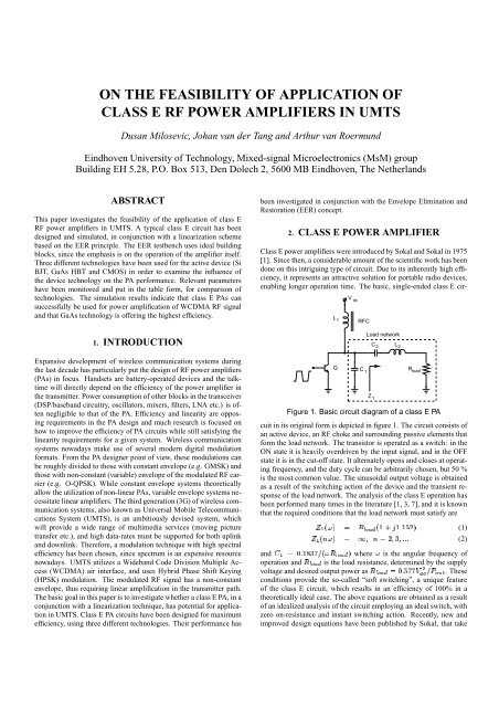
Figure 1. Basic circuit diagram <strong>of</strong> a <strong>class</strong> E PA<br />
cuit <strong>in</strong> its orig<strong>in</strong>al form is depicted <strong>in</strong> figure 1. The circuit c<strong>on</strong>sists <strong>of</strong><br />
an active device, an RF choke and surround<strong>in</strong>g passive elements that<br />
form <strong>the</strong> load network. The transistor is operated as a switch: <strong>in</strong> <strong>the</strong><br />
ON state it is heavily overdriven by <strong>the</strong> <strong>in</strong>put signal, and <strong>in</strong> <strong>the</strong> OFF<br />
state it is <strong>in</strong> <strong>the</strong> cut-<strong>of</strong>f state. It alternately opens and closes at operat<strong>in</strong>g<br />
frequency, and <strong>the</strong> duty cycle can be arbitrarily chosen, but 50 %<br />
is <strong>the</strong> most comm<strong>on</strong> value. The s<strong>in</strong>usoidal output voltage is obta<strong>in</strong>ed<br />
as a result <strong>of</strong> <strong>the</strong> switch<strong>in</strong>g acti<strong>on</strong> <strong>of</strong> <strong>the</strong> device and <strong>the</strong> transient resp<strong>on</strong>se<br />
<strong>of</strong> <strong>the</strong> load network. The analysis <strong>of</strong> <strong>the</strong> <strong>class</strong> E operati<strong>on</strong> has<br />
been pe<strong>rf</strong>ormed many times <strong>in</strong> <strong>the</strong> literature [1, 3, 7], and it is known<br />
that <strong>the</strong> required c<strong>on</strong>diti<strong>on</strong>s that <strong>the</strong> load network must satisfy are<br />
£¨§<br />
¢¡¤£¦¥¨§©<br />
£¥¨§© ©<br />
¡<br />
<br />
¡ ©£¦¥ §<br />
and<br />
¥<br />
where is <strong>the</strong> angular frequency <strong>of</strong><br />
operati<strong>on</strong><br />
<br />
and is <strong>the</strong> load resistance, determ<strong>in</strong>ed by <strong>the</strong> supply<br />
voltage and desired output <strong>power</strong><br />
© <br />
as . These<br />
c<strong>on</strong>diti<strong>on</strong>s provide <strong>the</strong> so-called “s<strong>of</strong>t switch<strong>in</strong>g”, a unique feature<br />
<strong>of</strong> <strong>the</strong> <strong>class</strong> E circuit, which results <strong>in</strong> an efficiency <strong>of</strong> 100% <strong>in</strong> a<br />
<strong>the</strong>oretically ideal case. The above equati<strong>on</strong>s are obta<strong>in</strong>ed as a result<br />
<strong>of</strong> an idealized analysis <strong>of</strong> <strong>the</strong> circuit employ<strong>in</strong>g an ideal switch, with<br />
zero <strong>on</strong>-resistance and <strong>in</strong>stant switch<strong>in</strong>g acti<strong>on</strong>. Recently, new and<br />
improved design equati<strong>on</strong>s have been published by Sokal, that take<br />
(1)<br />
(2)
<strong>in</strong>to account <strong>the</strong> <strong>in</strong>fluence <strong>of</strong> <strong>the</strong> transistor f<strong>in</strong>ite <strong>on</strong>-resistance, f<strong>in</strong>ite<br />
Q-factor <strong>of</strong> <strong>the</strong> load network and parasitic series resistances <strong>of</strong> passive<br />
elements <strong>on</strong> <strong>the</strong> output <strong>power</strong> and efficiency [2].<br />
3. CLASS E PA AND EER<br />
In <strong>the</strong> case <strong>of</strong> <strong>class</strong> E PAs, it is difficult to talk about l<strong>in</strong>earity, s<strong>in</strong>ce<br />
<strong>the</strong> circuit does not really pe<strong>rf</strong>orm an amplificati<strong>on</strong>: <strong>the</strong> <strong>in</strong>put signal<br />
is seen just as <strong>in</strong>formati<strong>on</strong> for trigger<strong>in</strong>g <strong>the</strong> active device, i.e. <strong>the</strong><br />
switch, and <strong>the</strong> amplitude <strong>of</strong> <strong>the</strong> output voltage is entirely determ<strong>in</strong>ed<br />
by <strong>the</strong> supply voltage and load network elements. In <strong>on</strong>e <strong>of</strong> his early<br />
papers Raab po<strong>in</strong>ts out that <strong>the</strong>se circuits are ra<strong>the</strong>r <strong>power</strong> c<strong>on</strong>verters<br />
than <strong>amplifiers</strong> [3]. Class E PAs are suitable <strong>on</strong>ly for c<strong>on</strong>stant envelope<br />
systems and any <strong>in</strong>formati<strong>on</strong> c<strong>on</strong>ta<strong>in</strong>ed <strong>in</strong> <strong>the</strong> amplitude <strong>of</strong> <strong>the</strong><br />
<strong>in</strong>put signal will be lost at <strong>the</strong> output. However, <strong>the</strong>re are ways to l<strong>in</strong>earize<br />
<strong>the</strong> operati<strong>on</strong> <strong>of</strong> <strong>the</strong> <strong>class</strong> E PA by mak<strong>in</strong>g use <strong>of</strong> <strong>the</strong> suitable<br />
l<strong>in</strong>earizati<strong>on</strong> technique. One l<strong>in</strong>earizati<strong>on</strong> scheme is called EER and<br />
its block diagram is given <strong>in</strong> figure 2. EER is particularly suitable<br />
RF <strong>in</strong>put<br />
Envelope detector<br />
Phase detector<br />
(limiter)<br />
V dc<br />
Amplitude<br />
modulator<br />
PA<br />
RF output<br />
Figure 2. Block diagram <strong>of</strong> <strong>the</strong> EER pr<strong>in</strong>ciple<br />
for <strong>class</strong> E PAs, s<strong>in</strong>ce all voltages <strong>in</strong> <strong>the</strong> load network <strong>of</strong> <strong>the</strong> <strong>class</strong><br />
E circuit are (<strong>in</strong> <strong>the</strong> ideal case) proporti<strong>on</strong>al to <strong>the</strong> supply voltage.<br />
Therefore, by chang<strong>in</strong>g <strong>the</strong> supply voltage it is possible to c<strong>on</strong>trol <strong>the</strong><br />
amplitude <strong>of</strong> <strong>the</strong> output signal. The <strong>in</strong>put signal, which has a variable<br />
envelope, is passed through <strong>the</strong> phase detector (limiter) and brought<br />
to <strong>the</strong> <strong>in</strong>put <strong>of</strong> <strong>the</strong> <strong>class</strong> E stage. Thus, <strong>the</strong> <strong>in</strong>formati<strong>on</strong> c<strong>on</strong>ta<strong>in</strong>ed <strong>in</strong><br />
<strong>the</strong> phase <strong>of</strong> <strong>the</strong> <strong>in</strong>put signal will be preserved <strong>in</strong> <strong>the</strong> output signal, and<br />
<strong>the</strong> envelope will be rec<strong>on</strong>structed through modulati<strong>on</strong> <strong>of</strong> <strong>the</strong> supply<br />
voltage. From a <strong>the</strong>oretical po<strong>in</strong>t <strong>of</strong> view, this is a pe<strong>rf</strong>ect c<strong>on</strong>cept: it<br />
comb<strong>in</strong>es l<strong>in</strong>ear <strong>power</strong> amplificati<strong>on</strong> with <strong>the</strong> high efficiency <strong>of</strong> <strong>the</strong><br />
<strong>class</strong> E amplifier. The output signal is a truthful replica <strong>of</strong> <strong>the</strong> <strong>in</strong>put<br />
signal, and <strong>the</strong> <strong>in</strong>herently high efficiency <strong>of</strong> <strong>the</strong> <strong>class</strong> E PA rema<strong>in</strong>s<br />
c<strong>on</strong>stant.<br />
4. CLASS E PA PERFORMANCE IN<br />
DIFFERENT TECHNOLOGIES<br />
In practice, <strong>the</strong> EER schematic will result <strong>in</strong> lower overall efficiency<br />
than <strong>the</strong> <strong>class</strong> E al<strong>on</strong>e, and <strong>the</strong> whole c<strong>on</strong>cept is attractive <strong>on</strong>ly if it<br />
can <strong>of</strong>fer superior efficiency to c<strong>on</strong>venti<strong>on</strong>al <strong>class</strong> A/AB <strong>power</strong> <strong>amplifiers</strong>,<br />
while still satisfy<strong>in</strong>g <strong>the</strong> l<strong>in</strong>earity requirements. Therefore, it<br />
is <strong>of</strong> high <strong>in</strong>terest to optimize <strong>the</strong> PA for <strong>the</strong> highest possible <strong>in</strong>tr<strong>in</strong>sic<br />
efficiency. Technology is <strong>on</strong>e <strong>of</strong> <strong>the</strong> crucial issues, and <strong>in</strong> this paper<br />
we have used three different devices to pe<strong>rf</strong>orm a technology benchmark<strong>in</strong>g:<br />
Si (<br />
<br />
BJT ), GaAs (¤<br />
<br />
HBT ) and<br />
CMOS18 ( <br />
<br />
technology ). The <strong>power</strong> <strong>amplifiers</strong> have<br />
been designed for operati<strong>on</strong> at 1.95 GHz, which corresp<strong>on</strong>ds to <strong>the</strong><br />
central frequency <strong>of</strong> <strong>the</strong> UMTS upl<strong>in</strong>k band (1920-1980 MHz), and<br />
with a target output <strong>power</strong> <strong>of</strong> approximately 500 mW (27 dBm). All<br />
three designs are based <strong>on</strong> <strong>the</strong> orig<strong>in</strong>al simple topology given <strong>in</strong> figure<br />
1, each with roughly optimized network elements, <strong>in</strong> order to take<br />
<strong>in</strong>to account different <strong>in</strong>tr<strong>in</strong>sic characteristics <strong>of</strong> <strong>the</strong> used devices. In<br />
this way c<strong>on</strong>diti<strong>on</strong>s for a fair comparis<strong>on</strong> <strong>of</strong> technologies are provided.<br />
Transistor siz<strong>in</strong>g is an important issue and <strong>the</strong> first step <strong>in</strong> <strong>the</strong> PA design.<br />
In <strong>the</strong> simulated PA designs, <strong>the</strong> devices were properly sized<br />
to give <strong>the</strong> desired output <strong>power</strong> and to avoid unrealistic high current<br />
densities that could result <strong>in</strong> reliability problems. Dimensi<strong>on</strong>s <strong>of</strong> <strong>the</strong><br />
BJT and <strong>the</strong> HBT have been chosen such that <strong>the</strong> peak current <strong>of</strong> <strong>the</strong><br />
device is below <strong>the</strong> value that corresp<strong>on</strong>ds to <strong>the</strong> ¤ maximum <strong>on</strong><br />
<strong>the</strong> <br />
<br />
vs. plot. A large MOS transistor has been used <strong>in</strong> order to<br />
provide low <strong>on</strong>-resistance and thus m<strong>in</strong>imize losses dur<strong>in</strong>g <strong>the</strong> ONstate.<br />
Before present<strong>in</strong>g <strong>the</strong> simulati<strong>on</strong> results, def<strong>in</strong>iti<strong>on</strong>s <strong>of</strong> some<br />
basic figures <strong>of</strong> merit for PAs will be given. Efficiency <strong>of</strong> a <strong>power</strong><br />
amplifier is def<strong>in</strong>ed as<br />
©<br />
<br />
(3)<br />
<br />
where is <strong>the</strong> output RF <strong>power</strong><br />
<br />
and is <strong>the</strong> supply <strong>power</strong>. This<br />
parameter is also referred to as output or collector/dra<strong>in</strong> efficiency.<br />
A more realistic measure <strong>of</strong> <strong>the</strong> amplifier’s pe<strong>rf</strong>ormance is <strong>the</strong> <strong>power</strong><br />
added efficiency (PAE), which takes <strong>in</strong>to account <strong>the</strong> <strong>in</strong>put <strong>power</strong>.<br />
PAE is def<strong>in</strong>ed as<br />
©<br />
<br />
(4)<br />
<br />
<br />
where is <strong>the</strong> <strong>in</strong>put <strong>power</strong> for <strong>the</strong> <strong>power</strong> amplifier. PAE significantly<br />
differs from when <strong>the</strong> <strong>power</strong> ga<strong>in</strong> is lower than 10 dB, for<br />
example, which is <strong>of</strong>ten <strong>the</strong> case with <strong>power</strong> <strong>amplifiers</strong>. S<strong>in</strong>ce <strong>the</strong><br />
<strong>power</strong> ga<strong>in</strong> <strong>of</strong> PAs is def<strong>in</strong>ed <br />
© <br />
as , <strong>the</strong> PAE also can<br />
be expressed as © £¤<br />
<br />
§<br />
. In all three designs, <strong>the</strong> tran-<br />
<br />
sistor <strong>in</strong>put term<strong>in</strong>al (base/gate) was driven by a s<strong>in</strong>usoidal voltage<br />
with <strong>the</strong> appropriate DC <strong>of</strong>fset. A similar approach has been used<br />
like <strong>in</strong> [4]. From a <strong>the</strong>oretical po<strong>in</strong>t <strong>of</strong> view, <strong>the</strong> ideal driv<strong>in</strong>g signal<br />
for <strong>class</strong> E PAs is a squarewave or trapezoidal voltage [2]. This is<br />
<strong>on</strong>e <strong>of</strong> major disadvantages <strong>of</strong> <strong>class</strong> E PAs, s<strong>in</strong>ce at frequencies <strong>in</strong><br />
GHz range, it is difficult to efficiently generate such pulses. For this<br />
reas<strong>on</strong>, a s<strong>in</strong>usoidal driv<strong>in</strong>g signal has been used, as an approximati<strong>on</strong><br />
and as a realistic opti<strong>on</strong>. Results <strong>of</strong> simulati<strong>on</strong>s are presented <strong>in</strong><br />
Table 1. Simulati<strong>on</strong> results for three Class E PAs<br />
Technology<br />
Parameter BJT HBT CMOS18<br />
Frequency (GHz) 1.95 1.95 1.95<br />
Supply voltage (V) 3 3 1.2<br />
Output <strong>power</strong> (mW) 498 482 410<br />
Output eff. <br />
<br />
<br />
(%) 79 89.6 79.6<br />
PAE (%) 75 86 -<br />
Power ga<strong>in</strong> (dB) 13.5 14.3 -<br />
Peak (V) 8.6 10.56 3.85<br />
Peak (mA) 480 556 1288<br />
Breakdown (V) 12 19 4<br />
600.0m 0.6<br />
Ic (A)<br />
400.0m 0.4<br />
200.0m 0.2<br />
0.00<br />
-200.0m −0.2<br />
12.0<br />
Vc (V) 10.0 10<br />
6.0<br />
6<br />
2.02<br />
−2<br />
zoom active<br />
-2.0<br />
156.6n<br />
156.6 156.8 156.8n<br />
157.0n<br />
157 157.2n 157.2<br />
157.4n<br />
157.4 157.6n t(ns)<br />
Figure 3. Simulated collector current and voltage<br />
table 1, and <strong>the</strong> characteristic <strong>class</strong> E waveforms for <strong>the</strong> PA employ<strong>in</strong>g<br />
an HBT are displayed <strong>in</strong> figure 3. First, it can be noticed from<br />
table 1 that a comparable pe<strong>rf</strong>ormance was achieved with all three<br />
devices. Output efficiency, , is close to 80% for circuits with BJT
and MOSFET, and almost 90% for <strong>the</strong> PA employ<strong>in</strong>g HBT. The drop<br />
<strong>in</strong> <strong>the</strong> efficiency from <strong>the</strong> <strong>the</strong>oretical 100% value is caused by several<br />
phenomena. A transistor can <strong>on</strong>ly approximate <strong>the</strong> switch<strong>in</strong>g acti<strong>on</strong>,<br />
and will exhibit f<strong>in</strong>ite turn-<strong>on</strong> and turn-<strong>of</strong>f transiti<strong>on</strong>s. Especially <strong>the</strong><br />
f<strong>in</strong>ite collector/dra<strong>in</strong> current fall time will have a detrimental effect.<br />
Thus, <strong>the</strong>re will be a certa<strong>in</strong> overlapp<strong>in</strong>g <strong>of</strong> n<strong>on</strong>-zero voltage and current<br />
that will <strong>in</strong>troduce losses. In additi<strong>on</strong>, <strong>the</strong> transistor has a f<strong>in</strong>ite<br />
<strong>on</strong>-resistance, which causes dissipati<strong>on</strong> dur<strong>in</strong>g <strong>the</strong> ON state <strong>of</strong> <strong>the</strong> RF<br />
cycle. In [6], it was shown that efficiency degrades with <strong>on</strong>-resistance<br />
as<br />
<br />
<br />
© <br />
where is <strong>the</strong> <strong>on</strong>-resistance <strong>of</strong> <strong>the</strong> transistor. Dur<strong>in</strong>g <strong>the</strong> ON state,<br />
a bipolar device (BJT or HBT) is <strong>in</strong> saturati<strong>on</strong>, and a MOS device<br />
is <strong>in</strong> l<strong>in</strong>ear (triode) regi<strong>on</strong>. Collector-to-emitter saturati<strong>on</strong> voltage,<br />
, depends <strong>on</strong> <strong>the</strong> actual type <strong>of</strong> <strong>the</strong> device under c<strong>on</strong>siderati<strong>on</strong>,<br />
<br />
but also <strong>on</strong> <strong>the</strong> frequency <strong>of</strong> operati<strong>on</strong> [2]. In circuits employ<strong>in</strong>g<br />
HBT and BJT it was around , and was somewhat lower<br />
<strong>in</strong> <strong>the</strong> CMOS PA. MOS model level 9 shows that <br />
for <strong>the</strong><br />
given transistor changes almost l<strong>in</strong>early from <br />
to <br />
when<br />
to and <strong>the</strong> gate is c<strong>on</strong>stantly driven with<br />
<br />
changes<br />
<br />
© from<br />
V. In <strong>the</strong> CMOS design, a very<br />
<br />
low has been used<br />
<strong>of</strong><br />
<br />
<strong>on</strong>ly . This is necessary because <strong>of</strong> <strong>the</strong> low supply voltage,<br />
which is imposed by <strong>the</strong> breakdown limitati<strong>on</strong> <strong>of</strong> <strong>the</strong> device (4V for<br />
<strong>the</strong> <strong>in</strong>tr<strong>in</strong>sic gate breakdown). Tak<strong>in</strong>g <strong>in</strong>to<br />
© <br />
account ,<br />
a good agreement is obta<strong>in</strong>ed between <strong>the</strong> simulated efficiency and<br />
<strong>the</strong> <strong>the</strong>oretical predicti<strong>on</strong> <strong>in</strong> (5). In table 1, PAE and <strong>power</strong> ga<strong>in</strong> for<br />
<strong>the</strong> CMOS circuit were omitted. Due to <strong>the</strong> impe<strong>rf</strong>ecti<strong>on</strong> <strong>of</strong> <strong>the</strong> active<br />
device model it was not possible to accurately determ<strong>in</strong>e <strong>the</strong> <strong>in</strong>put<br />
<strong>power</strong> for this design. MOS level 9 model was used. It does not<br />
model <strong>the</strong> <strong>in</strong>tr<strong>in</strong>sic resistance <strong>of</strong> <strong>the</strong> MOS device, that is seen by <strong>the</strong><br />
source driv<strong>in</strong>g <strong>the</strong> transistor. Namely, at high frequencies, <strong>the</strong> <strong>in</strong>put<br />
impedance <strong>of</strong> a MOS transistor is no l<strong>on</strong>ger purely capacitive, but<br />
has a real part as well, which is dissipat<strong>in</strong>g <strong>power</strong>. In [5] <strong>the</strong> relati<strong>on</strong><br />
between <strong>the</strong> <strong>in</strong>put <strong>power</strong>, series gate resistance and o<strong>the</strong>r transistor<br />
parameters was derived, but it was not taken <strong>in</strong>to account that apart<br />
from <strong>the</strong> series gate resistance, <strong>the</strong> MOS model has to <strong>in</strong>clude <strong>the</strong><br />
n<strong>on</strong>-quasi static resistance <strong>of</strong> <strong>the</strong> channel. Therefore, for accuracy<br />
reas<strong>on</strong>s, PAE and <strong>power</strong> ga<strong>in</strong> are not given <strong>in</strong> table 1 for <strong>the</strong> MOS<br />
PA.<br />
5. CLASS E AND WCDMA SIGNALS<br />
In figure 4, a block diagram <strong>of</strong> <strong>the</strong> l<strong>in</strong>earizati<strong>on</strong> c<strong>on</strong>cept based <strong>on</strong> <strong>the</strong><br />
EER pr<strong>in</strong>ciple is presented. WCDMA baseband signals I and Q are<br />
generated by <strong>the</strong> system simulator SPW, with a 3.84 Mcps chiprate,<br />
and imported <strong>in</strong>to <strong>the</strong> circuit simulator SpectreRF. The modulated RF<br />
I(t)<br />
Q(t)<br />
X 2<br />
X 2<br />
cos<br />
ω t<br />
c<br />
s<strong>in</strong> ω c t<br />
X<br />
v RF (t)<br />
1 X<br />
Figure 4. L<strong>in</strong>earizati<strong>on</strong> circuit<br />
signal is obta<strong>in</strong>ed by IQ modulati<strong>on</strong> as<br />
and can also be presented as<br />
£§©<br />
<br />
£§¤£¦¥§£§£¦¥§<br />
£§©£§£¦¥£§§<br />
E(t)<br />
v RF<strong>in</strong> (t)<br />
(5)<br />
(6)<br />
(7)<br />
This signal has a variable envelope (see fig. 6) and a peak-to-average<br />
<strong>power</strong> ratio (crest factor) <strong>of</strong> 5.7 dB. In <strong>the</strong> orig<strong>in</strong>al EER schematic,<br />
<strong>the</strong> envelope <strong>of</strong> <strong>the</strong> RF signal is obta<strong>in</strong>ed by pass<strong>in</strong>g it through <strong>the</strong><br />
amplitude detector, but it can also be d<strong>on</strong>e by <strong>the</strong> baseband signal<br />
process<strong>in</strong>g, as £§© £§ £§<br />
. The presented l<strong>in</strong>eariza-<br />
<br />
ti<strong>on</strong> scheme c<strong>on</strong>ta<strong>in</strong>s a m<strong>in</strong>or modificati<strong>on</strong> <strong>of</strong> <strong>the</strong> orig<strong>in</strong>al EER. The<br />
RF signal com<strong>in</strong>g from <strong>the</strong> IQ modulator is be<strong>in</strong>g multiplied by <strong>the</strong><br />
reciprocal value <strong>of</strong> <strong>the</strong> envelope. The underly<strong>in</strong>g idea is to generate<br />
<strong>the</strong> c<strong>on</strong>stant envelope s<strong>in</strong>usoidal signal with <strong>the</strong> preserved phase<br />
<strong>in</strong>formati<strong>on</strong> , i.e. zero cross<strong>in</strong>gs. Thus, a signal<br />
is obta<strong>in</strong>ed , which is more suitable for <strong>the</strong> <strong>class</strong> E PA, s<strong>in</strong>ce it was<br />
designed for a c<strong>on</strong>stant envelope s<strong>in</strong>ewave drive. From <strong>the</strong> l<strong>in</strong>eariza-<br />
£§©£¦¥£§§<br />
ti<strong>on</strong> circuitry, signals £§ and £§ are fed to <strong>the</strong> <strong>class</strong> E circuit,<br />
as depicted <strong>in</strong> figure 5. Signal £§<br />
is multiplied by <strong>the</strong> appro-<br />
v RF<strong>in</strong> (t)<br />
A<br />
E(t)<br />
V DC<strong>in</strong><br />
L 1<br />
Q<br />
C 1<br />
C 2<br />
L 2<br />
R load<br />
+<br />
v RFout (t)<br />
Figure 5. Class E PA with EER applied<br />
priate c<strong>on</strong>stant <br />
and a DC <strong>of</strong>fset voltage <br />
is added, <strong>in</strong> order to<br />
obta<strong>in</strong> <strong>the</strong> optimum driv<strong>in</strong>g signal for <strong>the</strong> active device. Values <strong>of</strong> <br />
and have been determ<strong>in</strong>ed for each device separately. Enve-<br />
lope signal £§<br />
is fed through a small <br />
¡<br />
<strong>in</strong>ductance . An RF choke<br />
can not be used <strong>in</strong> <strong>the</strong> circuit now, s<strong>in</strong>ce it would have a suppress<strong>in</strong>g<br />
effect <strong>on</strong> higher spectral comp<strong>on</strong>ents <strong>in</strong> £§ . In figure 6, <strong>the</strong> orig-<br />
3.0 v RF (t) [V]<br />
2.0<br />
1.0<br />
0<br />
−1.0<br />
−2.0<br />
−3.0<br />
3.0 v RFout (t) [V]<br />
2.0<br />
1.0<br />
0<br />
−1.0<br />
−2.0<br />
−3.0<br />
0 1 2 3 4 5<br />
t[μs]<br />
Figure 6. The orig<strong>in</strong>al and output WCDMA RF signal<br />
<strong>in</strong>al WCDMA RF signal and <strong>the</strong> output RF signal from <strong>the</strong> PA are<br />
given. Visual <strong>in</strong>specti<strong>on</strong> shows that <strong>the</strong> orig<strong>in</strong>al variable envelope is<br />
almost pe<strong>rf</strong>ectly restored <strong>in</strong> <strong>the</strong> output signal. The first 2 <strong>of</strong> <strong>the</strong><br />
simulati<strong>on</strong> should be neglected, until <strong>the</strong> WCDMA baseband generator<br />
enters <strong>the</strong> stable operati<strong>on</strong>. The ACPR measurements <strong>of</strong> <strong>the</strong> output<br />
signal show that <strong>the</strong> dem<strong>on</strong>strated operati<strong>on</strong> satisfies WCDMA<br />
requirements. The technical specificati<strong>on</strong> for WCDMA specifies <strong>the</strong><br />
m<strong>in</strong>imum ACPR ¡ =33 dBC and ACPR =43 dBc. The simulated pe<strong>rf</strong>ormance<br />
<strong>of</strong> <strong>the</strong> PA is given <strong>in</strong> <strong>the</strong> table 2. Power spectral densities<br />
Table 2. Simulated ACPR pe<strong>rf</strong>ormance <strong>of</strong> <strong>the</strong> l<strong>in</strong>earized PA<br />
Technology<br />
Parameter BJT HBT CMOS18<br />
ACPR ¡ (dBc) 39.7 34.4 37<br />
ACPR (dBc) 55.9 53.6 46.9<br />
(8)
used for calculati<strong>on</strong> <strong>of</strong> <strong>the</strong> ACPR are obta<strong>in</strong>ed from <strong>the</strong> results <strong>of</strong> 35<br />
<br />
transient simulati<strong>on</strong> <strong>in</strong> SpectreRF circuit simulator. The waveform<br />
<br />
calculator <strong>of</strong> Spectre RF has been used <strong>in</strong> calculati<strong>on</strong>s. In figure 7,<br />
<strong>the</strong> <strong>power</strong> spectrum <strong>of</strong> <strong>the</strong> output signal is displayed. It is impor-<br />
−10<br />
−30<br />
−50<br />
−70<br />
−90<br />
1.93<br />
Rel. <strong>power</strong> (dB)<br />
1.95<br />
1.97 f(GHz)<br />
Figure 7. Power spectral density <strong>of</strong> <strong>the</strong> output signal<br />
tant to note that all blocks <strong>in</strong> <strong>the</strong> l<strong>in</strong>earizati<strong>on</strong> schematic (multipliers,<br />
adders, square and square root functi<strong>on</strong>s) are ideal and do not <strong>in</strong>troduce<br />
any delay nor distorti<strong>on</strong>. This is <strong>of</strong> crucial importance, s<strong>in</strong>ce <strong>the</strong><br />
EER technique is particularly sensitive to delay mismatch <strong>in</strong> <strong>the</strong> envelope<br />
and phase path. The ACPR <strong>of</strong> £§ signal, generated by an<br />
ideal IQ modulator, is 65 dBc and 85 dBc, for ACPR ¡ and ACPR ,<br />
respectively. Therefore, <strong>the</strong> output signal exhibits a certa<strong>in</strong> degradati<strong>on</strong>,<br />
even though <strong>the</strong> build<strong>in</strong>g blocks <strong>in</strong> <strong>the</strong> EER circuit are ideal.<br />
Reas<strong>on</strong>s for such behaviour are multiple. First, <strong>the</strong> amplifier <strong>in</strong>troduces<br />
certa<strong>in</strong> amount <strong>of</strong> phase distorti<strong>on</strong>. Sec<strong>on</strong>dly, <strong>the</strong> assumpti<strong>on</strong><br />
that <strong>the</strong> amplitude <strong>of</strong> <strong>the</strong> output signal is l<strong>in</strong>early dependent <strong>on</strong> <strong>the</strong><br />
supply voltage does not hold <strong>in</strong> practice. Theoretically, <strong>the</strong> amplitude<br />
<strong>of</strong> <strong>the</strong> output signal from an ideal <strong>class</strong> E PA, supplied by <br />
, © <br />
is<br />
and <strong>the</strong><br />
<br />
ratio rema<strong>in</strong>s c<strong>on</strong>stant <br />
when<br />
changes [3]. This is not <strong>the</strong> case <strong>in</strong> practice, s<strong>in</strong>ce <strong>the</strong>re is <strong>the</strong><br />
entire set <strong>of</strong> voltage-dependent effects <strong>of</strong> a transistor, such as n<strong>on</strong>l<strong>in</strong>ear<br />
parasitic output capacitance. In figure 8, it is shown how <strong>the</strong><br />
amplitude <strong>of</strong> <strong>the</strong> output signal depends <strong>on</strong> <strong>the</strong> supply voltage, for <strong>the</strong><br />
PA based <strong>on</strong> <strong>the</strong> HBT. Factor is def<strong>in</strong>ed <br />
© <br />
as . It can be<br />
noticed that is smaller than <strong>the</strong> <strong>the</strong>oretical value <strong>of</strong> 1.074, which is<br />
expla<strong>in</strong>ed by <strong>the</strong> n<strong>on</strong>-idealities <strong>of</strong> a real circuit and <strong>in</strong>evitable losses.<br />
But <strong>the</strong><br />
<br />
n<strong>on</strong>-c<strong>on</strong>stant ratio is a more significant shortcom<strong>in</strong>g,<br />
s<strong>in</strong>ce it will have a direct impact <strong>on</strong> <strong>the</strong> l<strong>in</strong>earity and ACPR pe<strong>rf</strong>ormance.<br />
The PAE also changes with <strong>the</strong> supply voltage, and <strong>the</strong><br />
corresp<strong>on</strong>d<strong>in</strong>g plot for HBT based PA is given <strong>in</strong> figure 9.<br />
k 0.82<br />
0.78<br />
0.74<br />
0.7<br />
0.75<br />
1.2 1.65<br />
Figure 8. N<strong>on</strong>-c<strong>on</strong>stant<br />
PAE [%] 90<br />
80<br />
70<br />
60<br />
50<br />
40<br />
30<br />
20<br />
10<br />
2.1<br />
<br />
0.75 1.2 1.65 2.1<br />
2.55 3.0<br />
V DC [V]<br />
ratio <strong>in</strong> a <strong>class</strong> E PA<br />
2.55 3.0 VDC [V]<br />
Figure 9. PAE dependence <strong>on</strong> <strong>the</strong> supply voltage<br />
6. CONCLUSIONS<br />
In this paper results <strong>of</strong> an <strong>in</strong>vestigati<strong>on</strong> <strong>in</strong>to <strong>the</strong> <strong>class</strong> E PA capabilities<br />
for utilizati<strong>on</strong> <strong>in</strong> UMTS are presented. Class E circuits with three<br />
different active devices were designed and simulated. The results <strong>of</strong><br />
<strong>the</strong> simulati<strong>on</strong>s show that a comparable pe<strong>rf</strong>ormance is achieved with<br />
all three technologies, but <strong>the</strong> GaAs is <strong>the</strong> most promis<strong>in</strong>g opti<strong>on</strong>. A<br />
l<strong>in</strong>earizati<strong>on</strong> testbench based <strong>on</strong> <strong>the</strong> EER pr<strong>in</strong>ciple has been designed<br />
and applied, and <strong>the</strong> ACPR pe<strong>rf</strong>ormance was simulated. All three<br />
PAs exhibited pe<strong>rf</strong>ormance that satisfies <strong>the</strong> requirements prescribed<br />
by <strong>the</strong> UMTS standard. These simulati<strong>on</strong>s <strong>in</strong>dicate that <strong>class</strong> E PAs,<br />
given <strong>the</strong> appropriate signals from <strong>the</strong> l<strong>in</strong>earizati<strong>on</strong> circuitry are provided,<br />
can successfully be used for <strong>power</strong> amplificati<strong>on</strong> <strong>of</strong> WCDMA<br />
RF signal. Accord<strong>in</strong>g to our best knowledge, this is <strong>the</strong> first report<br />
<strong>in</strong> literature that quantitatively <strong>in</strong>vestigates <strong>the</strong> operati<strong>on</strong> <strong>of</strong> <strong>class</strong> E<br />
PAs for UMTS. The presented results <strong>in</strong>dicate that a fur<strong>the</strong>r <strong>in</strong>vestigati<strong>on</strong><br />
<strong>on</strong> this type <strong>of</strong> PAs and <strong>the</strong> l<strong>in</strong>earizati<strong>on</strong> circuits is <strong>of</strong> high<br />
importance. The ACPR pe<strong>rf</strong>ormance can be improved by add<strong>in</strong>g a<br />
predistorti<strong>on</strong> block <strong>in</strong> <strong>the</strong> envelope path, that would compensate <strong>the</strong><br />
n<strong>on</strong>l<strong>in</strong>earity caused by n<strong>on</strong>-c<strong>on</strong>stant factor. In practice, <strong>the</strong> n<strong>on</strong>idealities<br />
and limitati<strong>on</strong>s <strong>of</strong> <strong>the</strong> EER blocks will have negative effect <strong>on</strong><br />
<strong>the</strong> ACPR, and extensive research has to be d<strong>on</strong>e <strong>on</strong> <strong>the</strong> practical implementati<strong>on</strong>.<br />
Reduced efficiency <strong>of</strong> <strong>the</strong> <strong>class</strong> E stage at lower supply<br />
voltages <strong>in</strong>dicates that an advanced hybrid soluti<strong>on</strong> <strong>in</strong> <strong>the</strong> form <strong>of</strong> a<br />
comb<strong>in</strong>ati<strong>on</strong> <strong>of</strong> l<strong>in</strong>ear (e.g. <strong>class</strong> A) and switch<strong>in</strong>g type PA should be<br />
c<strong>on</strong>sidered, <strong>in</strong> order to obta<strong>in</strong> a satisfy<strong>in</strong>g overall efficiency pe<strong>rf</strong>ormance<br />
at all <strong>power</strong> levels.<br />
ACKNOWLEDGMENTS<br />
The work presented <strong>in</strong> this paper is funded by <strong>the</strong> Dutch technology<br />
foundati<strong>on</strong> STW. The authors would also like to thank Peter Baltus,<br />
Hans Hegt and P<strong>in</strong>g Wang for fruitful and c<strong>on</strong>structive discussi<strong>on</strong>s.<br />
7. REFERENCES<br />
[1] N. O. Sokal and A. D. Sokal, “Class E—A new <strong>class</strong> <strong>of</strong> highefficiency<br />
tuned s<strong>in</strong>gle-ended switch<strong>in</strong>g <strong>power</strong> <strong>amplifiers</strong>,”<br />
IEEE J. Solid-State Circuits, vol. SC-10, no. 6, pp. 168-176,<br />
June 1975.<br />
[2] N. O. Sokal, “Class-E switch<strong>in</strong>g-mode high-efficiency tuned<br />
RF/microwave <strong>power</strong> amplifier: improved design equati<strong>on</strong>s,”<br />
IEEE MTT-S Int. Microwave Symp. Digest, 2000, vol. 2 , pp.<br />
779-782.<br />
[3] F. H. Raab, “Idealized operati<strong>on</strong> <strong>of</strong> <strong>the</strong> <strong>class</strong> E tuned <strong>power</strong><br />
amplifier,” IEEE Transacti<strong>on</strong>s <strong>on</strong> Circuits and Systems, vol.<br />
CAS-24, no. 12, pp. 725-735, December 1977.<br />
[4] G. K. W<strong>on</strong>g and S. I. L<strong>on</strong>g, High efficiency bipolar <strong>power</strong><br />
amplifers, F<strong>in</strong>al Report 1997-98 for MICRO Project 97-104,<br />
see www.ucop.edu/research/micro/97 98/97 104.pdf<br />
[5] D. K. Choi and S. I. L<strong>on</strong>g, “A physically based analytic model<br />
<strong>of</strong> FET Class-E <strong>power</strong> <strong>amplifiers</strong>—design<strong>in</strong>g for maximum<br />
PAE,” IEEE Transacti<strong>on</strong>s <strong>on</strong> Microwave Theory and Techniques,<br />
vol. 47, no. 9, pp. 1712-1720, September 1999.<br />
[6] C. Yoo and Q. Huang, “A comm<strong>on</strong>-gate switched 0.9-W <strong>class</strong>-<br />
E <strong>power</strong> amplifier with 41 % PAE <strong>in</strong> 0.25- CMOS,” IEEE<br />
J. Solid-State Circuits, vol. 36, no. 5, pp. 823-830, May 2001.<br />
[7] S. C. Cripps, RF Power Amplifiers for Wireless Communicati<strong>on</strong>s,<br />
Artech House, 1999.