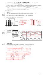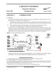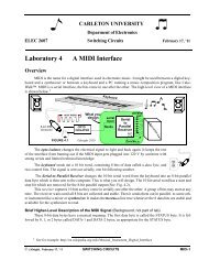
Laboratory 4 A MIDI Interface - Department of Electronics at Carleton ...
Laboratory 4 A MIDI Interface - Department of Electronics at Carleton ...
Laboratory 4 A MIDI Interface - Department of Electronics at Carleton ...

You also want an ePaper? Increase the reach of your titles
YUMPU automatically turns print PDFs into web optimized ePapers that Google loves.
<strong>Carleton</strong> University Description <strong>of</strong> the Blocks<br />
Description <strong>of</strong> the Blocks<br />
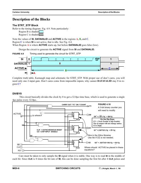
The STRT_STP Block<br />
Refer to the timing diagram Fig. 4.9. Note particularly:<br />
Region B is shaded .<br />
Region C is shaded .<br />
Note the values <strong>of</strong> SI, DATAVALID and ACTIVE in the regions A, B, and C.<br />
Region C is when SI is not active, th<strong>at</strong> is idle. See Fig. 4.4.<br />
When Region A is where ACTIVE starts up, but before DATAVALID goes false (low).<br />
Design the circuit to gener<strong>at</strong>e the ACTIVE signal from SI and DATAVALID.<br />
FIGURE 4.9 Timing used to gener<strong>at</strong>e the circuit for STRT_STP<br />
SI<br />
DATAVALID<br />
0<br />
1<br />
0<br />
ACTIVE<br />
B<br />
C<br />
A<br />
Complete truth table, Karnaugh map and schem<strong>at</strong>ic for STRT_STP. With proper use <strong>of</strong> don’t cares, you will<br />
need only one 2-input g<strong>at</strong>e. Don’t cares come from impossible inputs; why cannot DATAVALID stay 0 in region<br />
C?<br />
DIVBY8<br />
This circuit basically divides the clock by 8 to get a 32.0µs time base, which is used to gener<strong>at</strong>e a single<br />
4µs pulse every 32.0µs..<br />
ACTIVE<br />
CE<br />
CLK<br />
RST<br />
Q0<br />
Q1<br />
Q2<br />
to where?<br />
CLR = ASYNCHRONOUS RESET<br />
CE = CHIP INPUT ENABLE<br />
CARRY OUT “TC” ON 7 COUNT<br />
Care must be taken to only sample the SI signal when it is stable. One way is to read SI in the middle <strong>of</strong><br />
each bit. Since CLK is 8 times the bit r<strong>at</strong>e <strong>of</strong> SI, this can be done sampling the first bit after 4 CLK pulses and<br />
<strong>MIDI</strong>-6 SWITCHING CIRCUITS © J.Knight, March 1, ’06<br />
D<br />
C<br />
CE<br />
D<br />
C<br />
CE<br />
D<br />
C<br />
CE<br />
Q<br />
CLR<br />
Q<br />
CLR<br />
Q<br />
CLR<br />
TC<br />
Q0<br />
Q1<br />
Q2<br />
stop<br />
bit<br />
Q0 + = ( Q0 )·CE + Q0·CE<br />
On the flip-flops<br />
CE = Clock Enable (Chip Enable)<br />
The Q output will not change unless<br />
CE is high.<br />
1<br />
1<br />
FIGURE 4.10<br />
A 3-bit binary counter you<br />
will need to modify<br />
Q1 + =( Q0⊕Q1)·CE + Q1·CE<br />
fdce in the Xilinx libraries<br />
Use fdc if CE is not needed.<br />
Q2 + = (Q2⊕(Q1·Q0)·CE + Q2·CE<br />
Where should ACTIVE be placed in these<br />
equ<strong>at</strong>ions?