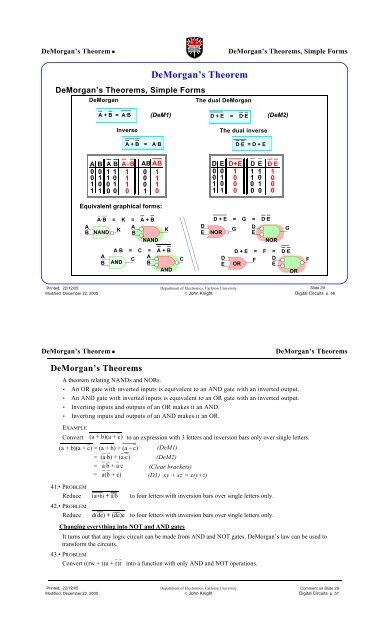
DeMorgan's Theorem - Department of Electronics at Carleton ...
DeMorgan's Theorem - Department of Electronics at Carleton ...
DeMorgan's Theorem - Department of Electronics at Carleton ...

Create successful ePaper yourself
Turn your PDF publications into a flip-book with our unique Google optimized e-Paper software.
DeMorgan’s <strong>Theorem</strong> DeMorgan’s <strong>Theorem</strong>s, Simple Forms<br />
DeMorgan’s <strong>Theorem</strong><br />
DeMorgan’s <strong>Theorem</strong>s, Simple Forms<br />
DeMorgan<br />
A + B = A·B<br />
A B A B A+B<br />
0<br />
0<br />
1<br />
1<br />
0<br />
1<br />
0<br />
1<br />
1 1<br />
1 0<br />
0 1<br />
0 0<br />
1<br />
1<br />
1<br />
0<br />
A<br />
B<br />
A<br />
B<br />
A + B = A·B<br />
(DeM1) D + E = D·E (DeM2)<br />
Inverse The dual inverse<br />
AB AB<br />
0 1<br />
0 1<br />
0 1<br />
1 0<br />
Equivalent graphical forms:<br />
A·B = K = A + B<br />
NAND<br />
K<br />
A<br />
B<br />
NAND<br />
K<br />
A·B = C = A + B<br />
AND<br />
C<br />
A<br />
B AND<br />
AND<br />
C<br />
The dual DeMorgan<br />
D E<br />
0 0<br />
0 1<br />
1 0<br />
1 1<br />
D·E = D + E<br />
D+E D E<br />
1<br />
0<br />
0<br />
0<br />
1 1<br />
1 0<br />
0 1<br />
0 0<br />
Printed; 22/12/05 <strong>Department</strong> <strong>of</strong> <strong>Electronics</strong>, <strong>Carleton</strong> University<br />
Slide 29<br />
Modified; December 22, 2005 © John Knight Digital Circuits p. 56<br />
D<br />
E<br />
D·E<br />
1<br />
0<br />
0<br />
0<br />
D + E = G = D·E<br />
NOR<br />
G<br />
D<br />
E<br />
NOR<br />
D<br />
E<br />
G<br />
D + E = F = D·E<br />
OR<br />
F<br />
D<br />
E<br />
OR<br />
DeMorgan’s <strong>Theorem</strong> DeMorgan’s <strong>Theorem</strong>s<br />
DeMorgan’s <strong>Theorem</strong>s<br />
A theorem rel<strong>at</strong>ing NANDs and NORs.<br />
• An OR g<strong>at</strong>e with inverted inputs is equivalent to an AND g<strong>at</strong>e with an inverted output.<br />
• An AND g<strong>at</strong>e with inverted inputs is equivalent to an OR g<strong>at</strong>e with an inverted output.<br />
• Inverting inputs and outputs <strong>of</strong> an OR makes it an AND.<br />
• Inverting inputs and outputs <strong>of</strong> an AND makes it an OR.<br />
EXAMPLE<br />
Convert (a + b)(a + c) to an expression with 3 letters and inversion bars only over single letters.<br />
(a + b)(a + c) = (a + b) + (a + c) (DeM1)<br />
41.• PROBLEM<br />
Reduce (a+b) + a·b to four letters with inversion bars over single letters only.<br />
42.• PROBLEM<br />
Reduce d(de) + (de)e to four letters with inversion bars over single letters only.<br />
Changing everything into NOT and AND g<strong>at</strong>es<br />
It turns out th<strong>at</strong> any logic circuit can be made from AND and NOT g<strong>at</strong>es. DeMorgan’s law can be used to<br />
transform the circuits.<br />
43.• PROBLEM<br />
= (a·b) + (a·c) (DeM2)<br />
= a·b + a·c<br />
= a(b + c)<br />
(Clear brackets)<br />
(D1) xy + xz = x(y+z)<br />
Convert ((rw + t)u + r)t into a function with only AND and NOT oper<strong>at</strong>ions.<br />
Printed; 22/12/05 <strong>Department</strong> <strong>of</strong> <strong>Electronics</strong>, <strong>Carleton</strong> University<br />
Comment on Slide 29<br />
Modified; December 22, 2005 © John Knight Digital Circuits p. 57<br />
F
DeMorgan’s <strong>Theorem</strong> Real CMOS Digital G<strong>at</strong>es<br />
Real CMOS Digital G<strong>at</strong>es<br />
Transistor NOT<br />
JOLT Small FREE Jolt JOLT Small FREE Jolt<br />
+V DD<br />
A<br />
Q 1<br />
Transistor NAND<br />
F<br />
E<br />
NAND<br />
VDD<br />
EF<br />
Two switches<br />
linked together<br />
F<br />
+<br />
+V DD<br />
A=1 => Q 1 closed => F=0<br />
E and F=1<br />
=>Output<br />
Grounded<br />
Output<br />
Inverted<br />
A<br />
B<br />
A<br />
Transistor NOR<br />
NOR<br />
VDD<br />
A+B<br />
Printed; 22/12/05 <strong>Department</strong> <strong>of</strong> <strong>Electronics</strong>, <strong>Carleton</strong> University<br />
Comment Slide 30 on Slide 1<br />
Modified; December 22, 2005 © John Knight Digital Circuits p. 58<br />
Q 1<br />
+5 V<br />
X X<br />
F<br />
B or A=1<br />
=>Output<br />
Grounded<br />
Output<br />
Inverted<br />
PMOS transistor acts like:<br />
closed switch when A is “0”<br />
open switch when A is “1”<br />
NMOS transistor acts like:<br />
open switch when A is “0”<br />
closed switch when A is “1”<br />
• One cannot make AND<br />
or OR g<strong>at</strong>es directly.<br />
• All CMOS G<strong>at</strong>es Invert<br />
• Real G<strong>at</strong>es are<br />
NAND, NOR and NOT<br />
DeMorgan’s <strong>Theorem</strong> DeMorgan’s <strong>Theorem</strong>s<br />
Constructing CMOS g<strong>at</strong>es from transistors<br />
DeMorgan’s <strong>Theorem</strong><br />
CMOS stands for Complementary Symmetry Metal-Oxide-Semiconductor g<strong>at</strong>es. They always have<br />
complementary transistors, which means PMOS (turn <strong>of</strong>f with a one input) above the output, and NMOS (turn<br />
on with a one input) below the output.<br />
The correct one inputs turn the lower NMOS transistors on, which<br />
pulls the output down to zero thus inverting the output.<br />
The Easily Constructed CMOS G<strong>at</strong>es<br />
NANDs with 2, 3 or 4 inputs, NORs with 2, 3 or 4 inputs, and NOTs.<br />
G<strong>at</strong>es constructed from other g<strong>at</strong>es<br />
To avoid all the extra inverters (NOTs) real circuits are designed to use<br />
NANDs and NORs instead <strong>of</strong> ANDs and ORs.<br />
Thinking<br />
• Thinking in NAND-NOR logic is difficult. Just look <strong>at</strong> any industrial schem<strong>at</strong>ic used extensively for<br />
maintenance. The margin will be full <strong>of</strong> “1”s and “0”s pencilled in by users.<br />
• Converting AND-OR into NAND-NOR is a straightforward mechanical process.<br />
• Much less error prone than doing logic with inverted signals 1 and NAND-NOR logic.<br />
These Notes<br />
• If the logic is important ANDs and ORs will be used.<br />
• If the g<strong>at</strong>e design is important, as when we talk about CMOS g<strong>at</strong>es, NANDs and NORs will be used.<br />
1. If “flash” is a signal name, “flash” is an inverted signal.<br />
How an OR<br />
is made<br />
Printed; 22/12/05 <strong>Department</strong> <strong>of</strong> <strong>Electronics</strong>, <strong>Carleton</strong> University<br />
Comment on Slide 30<br />
Modified; December 22, 2005 © John Knight Digital Circuits p. 59<br />
a<br />
b<br />
How an AND<br />
is made<br />
One way <strong>of</strong> making an XOR<br />
See problem 41.<br />
a⊕b
DeMorgan’s <strong>Theorem</strong> Real CMOS Digital G<strong>at</strong>es<br />
Using DeMorgan’s <strong>Theorem</strong><br />
AND<br />
AND<br />
Equivalent G<strong>at</strong>e Symbols<br />
NAND<br />
NAND<br />
Real G<strong>at</strong>es are NAND and NOR Easy to Understand G<strong>at</strong>es<br />
are AND and OR<br />
NAND<br />
AND<br />
NOR<br />
One cannot make AND and<br />
OR g<strong>at</strong>es directly.<br />
a<br />
b<br />
c<br />
d<br />
NAND<br />
NAND<br />
NAND<br />
Which one is easier for you to understand?<br />
Printed; 22/12/05 <strong>Department</strong> <strong>of</strong> <strong>Electronics</strong>, <strong>Carleton</strong> University<br />
Slide 31<br />
Modified; December 22, 2005 © John Knight Digital Circuits p. 60<br />
NOR<br />
AND OR<br />
Circuit with real g<strong>at</strong>es Circuit with simple g<strong>at</strong>es<br />
F = (ab) • (cd)<br />
F<br />
NOR<br />
a<br />
b<br />
c<br />
d<br />
AND<br />
AND<br />
F = ab + cd<br />
DeMorgan’s <strong>Theorem</strong> DeMorgan’s <strong>Theorem</strong>s<br />
DeMorgan’s <strong>Theorem</strong><br />
The two expressions for the circuit with real g<strong>at</strong>es and the circuit with simple g<strong>at</strong>es, are equivalent<br />
Use High-True And-Or Signals for Thinking<br />
Thinking<br />
• Thinking in nand-nor logic is difficult. Just look <strong>at</strong> any industrial schem<strong>at</strong>ic used extensively for<br />
maintenance. The margin will be full <strong>of</strong> “1”s and “0”s pencilled in by users.<br />
• Converting between and-or and nand-nor is a straightforward mechanical process.<br />
• Much less error prone than doing logic with asserted low signals and nand-nor logic.<br />
These Notes<br />
ab + cd = F = (ab) • (cd)<br />
• If the logic is important ANDs and ORs will be used.<br />
• If the g<strong>at</strong>e design is important, as when we talk about CMOS g<strong>at</strong>es, NANDs and NORs will be used.<br />
44.• PROBLEM<br />
Prove, using DeMorgan’s Theroem(s), th<strong>at</strong><br />
ab + cd = (ab) • (cd)<br />
Printed; 22/12/05 <strong>Department</strong> <strong>of</strong> <strong>Electronics</strong>, <strong>Carleton</strong> University<br />
Comment on Slide 31<br />
Modified; December 22, 2005 © John Knight Digital Circuits p. 61<br />
OR<br />
F<br />
OR<br />
OR
DeMorgan’s <strong>Theorem</strong> Circuits Using NANDs and NORS are<br />
Circuits Using NANDs and NORS are Hard to Follow<br />
Example<br />
Don’t do thinking with NANDs and NORs.<br />
Confusing multiple logic inversions.<br />
Does w<strong>at</strong>er stop or start the train?<br />
Is SW1 a start or stop switch?<br />
SW1<br />
PWR<br />
AIR<br />
DOOROPN1<br />
DOOROPN2<br />
WATER<br />
U1.1<br />
U1.2<br />
U1.3<br />
Do Thinking Part <strong>of</strong> Design with AND/OR;<br />
Convert After Thinking is Done<br />
SW1·PWR + AIR·(DOOROPN1·DOOROPN2) + WATER<br />
The same circuit made with ANDs and ORs.<br />
The final equ<strong>at</strong>ion can be written from inspection. (Is there a logic error?)<br />
SW1<br />
PWR<br />
AIR<br />
DOOROPN1<br />
DOOROPN2<br />
WATER<br />
Printed; 22/12/05 <strong>Department</strong> <strong>of</strong> <strong>Electronics</strong>, <strong>Carleton</strong> University<br />
Slide 32<br />
Modified; December 22, 2005 © John Knight Digital Circuits p. 62<br />
U3.1<br />
Start_O-Train<br />
Start_O-Train<br />
SW1·PWR·AIR·(DOOROPN1 + DOOROPN2)·WATER<br />
DeMorgan’s <strong>Theorem</strong> Starting The O-Train<br />
Starting The O-Train 1<br />
The AND-OR logic is much clearer. It takes air, power, w<strong>at</strong>er to start the train. Also two doors must not be<br />
open. However it takes 4 g<strong>at</strong>es and 6 inverters to implement the AND-OR circuit made by adding inverters to<br />
NANDs and NORs. The less clear NAND-NOR circuit does the same logic, with 4 g<strong>at</strong>es and 1 inverter.<br />
NAND-NOR Logic is Confusing to Humans<br />
Multiple neg<strong>at</strong>ives are confusing<br />
If your teacher said, “Never will I not, not give you a A in Digital Circuits,” it would take you some careful<br />
reading to determine your mark.<br />
Diagrams with real g<strong>at</strong>es<br />
This is the kind <strong>of</strong> diagram one would use to build a circuit.<br />
It has easily manufacturable g<strong>at</strong>es, i.e. NOT, NAND and NOR.<br />
The numbers U1.1 etc. are g<strong>at</strong>e numbers th<strong>at</strong> would physically identify the g<strong>at</strong>e on a layout diagram showing<br />
where each part was.<br />
Easy to read diagrams<br />
You should be able to spot the logic error.<br />
DOOROPN1 + DOOROPN2<br />
Should you be able to start the train with one door open?<br />
1. The O-Train is an Ottawa interurban train, which stops right outside the Engineering Building <strong>at</strong> <strong>Carleton</strong> University.<br />
Printed; 22/12/05 <strong>Department</strong> <strong>of</strong> <strong>Electronics</strong>, <strong>Carleton</strong> University<br />
Comment on Slide 32<br />
Modified; December 22, 2005 © John Knight Digital Circuits p. 63
DeMorgan’s <strong>Theorem</strong> DeMorgan Transfers Real G<strong>at</strong>es Into<br />
DeMorgan Transfers Real G<strong>at</strong>es Into Simple G<strong>at</strong>es<br />
Circuit with real g<strong>at</strong>es Circuit with simple g<strong>at</strong>es<br />
a<br />
b<br />
c<br />
d<br />
NAND<br />
NAND<br />
NAND<br />
F = (ab) • (cd)<br />
• Circuits meant for understanding the logic use ANDs and ORs.<br />
- Draw your circuits with ANDs and ORs.<br />
• Circuits for construction are drawn with NANDs and NORs.<br />
Draw construction diagrams by:<br />
F<br />
NAND<br />
NAND<br />
NAND<br />
Use DeMorgan’s NAND<br />
g<strong>at</strong>e symbol <strong>at</strong> output<br />
- transforming the understandable circuit into the real circuit<br />
- using the DeMorgan altern<strong>at</strong>e symbols.<br />
NAND<br />
NAND<br />
• Thus Compromise drawings have NANDS and NORs<br />
with the circles are arranged to cancel each other.<br />
NAND<br />
Inverting circles<br />
cancel each other<br />
Printed; 22/12/05 <strong>Department</strong> <strong>of</strong> <strong>Electronics</strong>, <strong>Carleton</strong> University<br />
Slide 33<br />
Modified; December 22, 2005 © John Knight Digital Circuits p. 64<br />
a<br />
b<br />
c<br />
d<br />
NAND<br />
NAND<br />
AND<br />
AND<br />
OR<br />
F = ab + cd<br />
NAND<br />
altern<strong>at</strong>e<br />
NAND<br />
symbol<br />
DeMorgan’s <strong>Theorem</strong> Transforming NAND-NOR Diagrams into<br />
Transforming NAND-NOR Diagrams into AND-OR Diagrams<br />
• Diagrams in this course will be drawn with ANDs and ORs as much as possible.<br />
• Diagrams for construction or maintainance, th<strong>at</strong> want to show exactly wh<strong>at</strong> g<strong>at</strong>es were used, will be<br />
drawn with NANDs and NORs. This is particularly true <strong>of</strong> older diagrams.<br />
• A compromise method, which is almost as easy to follow, but shows<br />
the real g<strong>at</strong>es as used, is to make altern<strong>at</strong>e g<strong>at</strong>es with the altern<strong>at</strong>e<br />
symbols, the ones with the inverting circles on the inputs.<br />
NOR NAND<br />
NOTE:<br />
One output circle cancels all the input circles it feeds.<br />
45.• PROBLEM<br />
Transform this circuit into simple g<strong>at</strong>es.<br />
a)<br />
Printed; 22/12/05 <strong>Department</strong> <strong>of</strong> <strong>Electronics</strong>, <strong>Carleton</strong> University<br />
Comment on Slide 33<br />
Modified; December 22, 2005 © John Knight Digital Circuits p. 65<br />
F
Don’t do initial design in NANDs and DeMorgan Transfers Real G<strong>at</strong>es Into<br />
R<strong>at</strong>ional<br />
Don’t do initial design in NANDs and NORs.<br />
Design in AND/OR;<br />
Convert After Thinking is Done<br />
• People think best with AND and OR.<br />
• Multiple inversions are very confusing<br />
• There is seldom a logical reason to invert except <strong>at</strong> circuit inputs.<br />
• Conversion AND/OR ⇒ NAND/NOR is easy using DeMorgan’s form <strong>of</strong> g<strong>at</strong>es.<br />
Do it after the thinking is done.<br />
Some people still seem to prefer designing with NANDs and NORs<br />
but not in this class<br />
Printed; 22/12/05 <strong>Department</strong> <strong>of</strong> <strong>Electronics</strong>, <strong>Carleton</strong> University<br />
Slide 34<br />
Modified; December 22, 2005 © John Knight Digital Circuits p. 66<br />
Don’t do initial design in NANDs and Design With Conceptually Easy Logic<br />
Design With Conceptually Easy Logic<br />
In the post 2000 era, people usually think about the logic. The details <strong>of</strong> construction are done autom<strong>at</strong>ically.<br />
This means you will normally do AND-OR type logic.<br />
Think with AND-OR<br />
Build with NAND-NOR<br />
DeMorgan’s Law Transforms Real G<strong>at</strong>es to Simple G<strong>at</strong>es<br />
46.• PROBLEM<br />
Transform this circuit into simple g<strong>at</strong>es.<br />
Printed; 22/12/05 <strong>Department</strong> <strong>of</strong> <strong>Electronics</strong>, <strong>Carleton</strong> University<br />
Comment on Slide 34<br />
Modified; December 22, 2005 © John Knight Digital Circuits p. 67
Don’t do initial design in NANDs and AND/OR to NAND/NOR Conversion<br />
AND/OR to NAND/NOR Conversion<br />
Example using graphical form<br />
1. Start with AND/OR circuit<br />
F = (a + c)(b + c) + cd<br />
2. Select altern<strong>at</strong>e connection layers.<br />
(Every second layer <strong>of</strong> connecting wires<br />
between layers <strong>of</strong> g<strong>at</strong>es.)<br />
One end <strong>of</strong> wires may be inputs or outputs.<br />
3. Put back-to-back inverting circles on both<br />
ends <strong>of</strong> the leads.<br />
Add NOT g<strong>at</strong>es when necessary ((a), (b)<br />
and (c))<br />
4. Moving inverters, or inverting bubbles may<br />
make logic simpler.<br />
• Sometimes inverters on two (or more) input<br />
leads should be moved to the output.<br />
(See next example)<br />
Printed; 22/12/05 <strong>Department</strong> <strong>of</strong> <strong>Electronics</strong>, <strong>Carleton</strong> University<br />
Slide 35<br />
Modified; December 22, 2005 © John Knight Digital Circuits p. 68<br />
Don’t do initial design in NANDs and Converting AND/OR Designs to NAND/<br />
Converting AND/OR Designs to NAND/NOR<br />
input<br />
b<br />
c<br />
a<br />
d<br />
skip<br />
1. Start with an AND-OR circuit. If you are starting with an equ<strong>at</strong>ion. draw the circuit.<br />
• The original formula will usually have inversions only on inputs. However there may be inversions anywhere.<br />
2. The circuit is drawn with a layer <strong>of</strong> connections which feeds a<br />
layer <strong>of</strong> g<strong>at</strong>es, feeding a layer <strong>of</strong> connections (green), which<br />
feeds another layer <strong>of</strong> g<strong>at</strong>es, which feeds another layer <strong>of</strong><br />
connections (green). Some circuits may have more or fewer<br />
layers. Select altern<strong>at</strong>e connection layers.<br />
• Some circuits are nicely layered with the first layer<br />
feeding a second layer which feeds a third layer etc. However this step is not exact. There are <strong>of</strong>ten<br />
several legitim<strong>at</strong>e ways to define layers. Note some wires, like (a) and (b) may pass through a g<strong>at</strong>e<br />
level (green) without a g<strong>at</strong>e.<br />
3. Put back-to-back inverting circles <strong>at</strong> both ends <strong>of</strong> wires going through a connection layer. On leads like (a)<br />
and (b), you will have to add an inverter, since there is no g<strong>at</strong>e on which to place the second circle.<br />
4. This step is less autom<strong>at</strong>ic. Look for leads where two inverters can be replaced by one. When doing this be<br />
careful not to invert a other connections on the same input, like (h). When moving inverting circles make<br />
sure th<strong>at</strong> the number <strong>of</strong> circles between the signal input and all the g<strong>at</strong>e inputs it goes to, are the same before<br />
and after moving.<br />
1<br />
BEFORE AFTER<br />
2<br />
3)<br />
Number <strong>of</strong> inversions<br />
from input to this g<strong>at</strong>e input<br />
Printed; 22/12/05 <strong>Department</strong> <strong>of</strong> <strong>Electronics</strong>, <strong>Carleton</strong> University<br />
Comment on Slide 35<br />
Modified; December 22, 2005 © John Knight Digital Circuits p. 69<br />
1<br />
(h)<br />
2<br />
(a)<br />
(h)<br />
4)<br />
(b)<br />
(b)<br />
(a)<br />
skip<br />
Number <strong>of</strong> inversions<br />
from input to this g<strong>at</strong>e input<br />
3)<br />
4)<br />
2)<br />
1)<br />
F<br />
(c)
Don’t do initial design in NANDs and AND/OR to NAND/NOR Conversion<br />
AND/OR to NAND/NOR Conversion<br />
4. Copy <strong>of</strong> step 4 on last slide:<br />
It has back-to-back bubbles<br />
and consolid<strong>at</strong>ed inverters<br />
5. Select the unconventional g<strong>at</strong>es.<br />
The ones with input bubbles.<br />
This is a compromise solution which is:<br />
• fairly readable<br />
• represents real g<strong>at</strong>es<br />
6. Use DeMorgan laws on the<br />
unconventional g<strong>at</strong>es.<br />
• Hard to understand the logic<br />
• but good for construction.<br />
Printed; 22/12/05 <strong>Department</strong> <strong>of</strong> <strong>Electronics</strong>, <strong>Carleton</strong> University<br />
Slide 36<br />
Modified; December 22, 2005 © John Knight Digital Circuits p. 70<br />
b<br />
c<br />
a<br />
d<br />
NOR<br />
NAND<br />
NAND<br />
Don’t do initial design in NANDs and Converting AND/OR Designs to NAND/<br />
On previous slide<br />
• You must always add two inverting circles to a lead, or none. Never add just one circle, not even if one<br />
exists already.<br />
On this slide<br />
5. Look <strong>at</strong> the g<strong>at</strong>es. Conventional ones have circles on their outputs and are NANDs, NORs or NOTs.<br />
The unconventional ones have circles on their inputs but are still NANDs, NORs or NOTs.<br />
• This step gives a circuit which is fairly easy to read because one can mentally cancel the back-to-back<br />
circles. However it still represents a circuit you can build easily because it does not contain ANDs and<br />
ORs.<br />
6. If desired, one can replace the DeMorgan forms <strong>of</strong> NOR and NAND, the<br />
ones with circles on the inputs, with the more standard forms with a circle<br />
on the output.<br />
• Since NAND-NOR diagrams represent real g<strong>at</strong>es, do not place a single circle on the input <strong>of</strong> a g<strong>at</strong>e, as<br />
was done in the theoretical AND-OR diagram.<br />
47.• PROBLEM:.<br />
For the circuit on the right, find the NAND-NOR circuit when<br />
the connection on the levels shown are selected.<br />
A<br />
B<br />
C<br />
D<br />
E<br />
H<br />
G<br />
F<br />
48.• PROBLEM<br />
Printed; 22/12/05 <strong>Department</strong> <strong>of</strong> <strong>Electronics</strong>, <strong>Carleton</strong> University<br />
Comment on Slide 36<br />
Modified; December 22, 2005 © John Knight Digital Circuits p. 71<br />
NOR<br />
Find an AND-OR equivalent for the circuit on the left.<br />
This requires working backwards.<br />
4)<br />
5)<br />
6)<br />
F<br />
F<br />
G
Don’t do initial design in NANDs and 2nd Example <strong>of</strong> AND/OR to NAND/NOR<br />
2nd Example <strong>of</strong> AND/OR to NAND/NOR<br />
b<br />
c<br />
a<br />
d<br />
1) AND/OR circuit; F = (a + c)(b + c) + cd<br />
3) Add cancelling back-to-back inverting circles<br />
add inverters where necessary.<br />
5) Select the unconventional g<strong>at</strong>es.<br />
F<br />
2) Select every other connection levels<br />
4) Input inverters pairs may become single<br />
inverters if moved to the g<strong>at</strong>e output<br />
F<br />
b<br />
c<br />
a<br />
F<br />
6) DeMorgan conventional g<strong>at</strong>es (optional).<br />
Compromise Answer Conventional (Dinosaur) Answer<br />
Printed; 22/12/05 <strong>Department</strong> <strong>of</strong> <strong>Electronics</strong>, <strong>Carleton</strong> University<br />
Slide 37<br />
Modified; December 22, 2005 © John Knight Digital Circuits p. 72<br />
Don’t do initial design in NANDs and AND/OR NAND/NOR Conversion<br />
AND/OR ⇐⇒ NAND/NOR Conversion (cont)<br />
This is the same circuit as the previous example.<br />
The difference between the examples starts <strong>at</strong> step 2<br />
Printed; 22/12/05 <strong>Department</strong> <strong>of</strong> <strong>Electronics</strong>, <strong>Carleton</strong> University<br />
Comment on Slide 37<br />
Modified; December 22, 2005 © John Knight Digital Circuits p. 73<br />
d<br />
SKIP<br />
2. the altern<strong>at</strong>e blocks <strong>of</strong> leads where the inverters are added are th<strong>at</strong> ones marked SKIP in the first example.<br />
Compare step 2 here with step 2 on Slide 35.<br />
3. In this step, the two inverters feeding the OR with inverting inputs looks too complex.<br />
Throwing out the double circles leaves us with an OR g<strong>at</strong>e. This is not allowed.<br />
Go to the output <strong>of</strong> the OR and add back-to-back inversions there. This gives a NOR g<strong>at</strong>e which is allowed.<br />
Both the lower g<strong>at</strong>es on the right are<br />
equivalent to an OR g<strong>at</strong>e, but one is<br />
simpler to implement as real g<strong>at</strong>es.<br />
Equivalent g<strong>at</strong>es<br />
6. Changing the NORs and NANDs with circles on their inputs, to NORs and NANDs with circles on their<br />
outputs, is the final step. Do it if you like such drawings better, or if the drawing standards your company<br />
uses require it, or if your boss says to.<br />
• Compare the results with those in steps 5 and 6 <strong>of</strong> the previous example. This circuit is marginally<br />
simpler than the previous result. One NOT g<strong>at</strong>e is saved.<br />
F
DeMorgan’s <strong>Theorem</strong>s, General Form 2nd Example <strong>of</strong> AND/OR to NAND/NOR<br />
DeMorgan’s <strong>Theorem</strong>s, General Form<br />
Abstract Form<br />
F(A,B,C, . . . +, ·,) = F(A,B,C, . . . ,·, +,)<br />
Action Example I<br />
a) Take a Boolean expression<br />
b) Bracket all groups <strong>of</strong> ANDs<br />
Take dual<br />
c) Change AND → OR and OR → AND<br />
d) Clean brackets<br />
Change dual into inverse<br />
e) Invert all variables<br />
F = A·B·C<br />
F = {A·B·C}<br />
F dual = {A + B + C}<br />
F dual = A + B + C<br />
F = {A + B + C}<br />
Printed; 22/12/05 <strong>Department</strong> <strong>of</strong> <strong>Electronics</strong>, <strong>Carleton</strong> University<br />
Slide 38<br />
Modified; December 22, 2005 © John Knight Digital Circuits p. 74<br />
DeMorgan’s <strong>Theorem</strong>s, General Form General Form <strong>of</strong> DeMorgan’s <strong>Theorem</strong><br />
General Form <strong>of</strong> DeMorgan’s <strong>Theorem</strong><br />
The slide shows a simplified version<br />
The true generalized DeMorgan<br />
F(A,B,C, . . . +, ·,0,1) = F(A,B,C, . . . ,·, +,1,0)<br />
F(A,B,C, . . . +, ·,0,1) = F(A,B,C, . . . ,·, +,1,0)<br />
The interchange <strong>of</strong> 0 and 1 was left out on the slide, since designers practically never have 0 or 1 in the<br />
expressions they oper<strong>at</strong>e on with DeMorgan’s law.<br />
DeMorgan’ general law is very similar to Duality<br />
The obvious difference is the inverting bars.<br />
Another important difference is the applic<strong>at</strong>ion.<br />
• DeMorgan transforms an expression into its inverse.<br />
• Duality takes a valid identity and gener<strong>at</strong>es another valid identity.<br />
49.• PROBLEM<br />
Find an expression for F th<strong>at</strong> has inverting bars only over single letters,<br />
F = (a + c)(b + c) + cd<br />
Printed; 22/12/05 <strong>Department</strong> <strong>of</strong> <strong>Electronics</strong>, <strong>Carleton</strong> University<br />
Comment on Slide 38<br />
Modified; December 22, 2005 © John Knight Digital Circuits p. 75
Examples: Generalized DeMorgan’s 2nd Example <strong>of</strong> AND/OR to NAND/NOR<br />
Example II<br />
Examples: Generalized DeMorgan’s <strong>Theorem</strong>s<br />
b) Bracket all groups <strong>of</strong> ANDs<br />
F(A,B,C, . . . +, ·,) = F(A,B,C, . . . ,·, +,)<br />
a) Take a Boolean expression F = A·B·C + A·B<br />
Take dual<br />
c) Change AND → OR and OR → AND<br />
e) Clean brackets<br />
Change dual into inverse<br />
e) Invert all variables<br />
Example III<br />
a) Take any Boolean expression<br />
b) Bracket all groups <strong>of</strong> ANDs<br />
c) Change AND →OR and OR →AND<br />
Ignore any existing overbars<br />
d) Clean brackets<br />
e) Invert all variables<br />
{A·B·C} + {A·B }<br />
F dual = {A+B+C}·{A+B }<br />
F dual = (A+B+C)·(A+B )<br />
F = (A+B+C)·(A+B )<br />
F = [A·B·C + D·(A·B + C)]·A<br />
F = {[ {A·B·C } + {D·( {A·B} + C)} ]·A}<br />
F dual = {[{A + B + C}·{D + ({A + B}·C)}] + A}<br />
F dual = {A + B + C}·{D + {A + B}·C} + A<br />
F = {A + B + C}·{D + {A + B}·C} + A<br />
Printed; 22/12/05 <strong>Department</strong> <strong>of</strong> <strong>Electronics</strong>, <strong>Carleton</strong> University<br />
Slide 39<br />
Modified; December 22, 2005 © John Knight Digital Circuits p. 76<br />
Examples: Generalized DeMorgan’s Examples using the Generalized<br />
Examples using the Generalized DeMorgan’s Law<br />
Be sure to put brackets around the ANDs<br />
When you do algebra, you autom<strong>at</strong>ically do the ANDs before the ORs. The not<strong>at</strong>ion is designed th<strong>at</strong> way.<br />
Putting brackets around an OR shows th<strong>at</strong> the OR should be done before the AND.<br />
When you use DeMorgan’s law, and you transform<br />
ab + cd into (a+b)(c+d),<br />
the brackets make sure th<strong>at</strong> the variables in the transformed expression are oper<strong>at</strong>ed on in the same order. Th<strong>at</strong><br />
is you don’t try to do a(b + c)d.<br />
By placing the brackets around the ANDs first, you do not get confused during the transform<strong>at</strong>ions.<br />
50.• PROBLEM<br />
(a) Convert (a + b)(a + c) to an expression with 3 letters and inversion bars only over single letters, using the<br />
Generalized DeMorgan’s law.<br />
(b) Compare this method with th<strong>at</strong> <strong>of</strong> the Example on Comment on Slide 29 and see if the algebra is shorter.<br />
Printed; 22/12/05 <strong>Department</strong> <strong>of</strong> <strong>Electronics</strong>, <strong>Carleton</strong> University<br />
Comment on Slide 39<br />
Modified; December 22, 2005 © John Knight Digital Circuits p. 77
Examples: Generalized DeMorgan’s Examples: Generalized DeMorgan’s<br />
Examples: Generalized DeMorgan’s <strong>Theorem</strong>s<br />
Note:<br />
Example IV<br />
a) Take a Boolean expression F = A·B·C + A·B<br />
b) Bracket all groups <strong>of</strong> ANDs<br />
c) Change AND → OR and OR → AND<br />
Ignore existing overbars<br />
d) Clean brackets if convenient<br />
e) Invert all variables<br />
Ignore any inverting overbars except over single letters<br />
{A·B·C} + {A·B }<br />
F dual = {A+B+C}·{A+B }<br />
F dual = (A+B+C)·(A+B )<br />
F = (A+B+C)·(A+B)<br />
F = A·B·(C + A·B) F dual = {A·B}·(C+ { A·B }) F = {A+B}+(C·{ A+B })<br />
Printed; 22/12/05 <strong>Department</strong> <strong>of</strong> <strong>Electronics</strong>, <strong>Carleton</strong> University<br />
Slide 40<br />
Modified; December 22, 2005 © John Knight Digital Circuits p. 78<br />
Examples: Generalized DeMorgan’s Examples using the Generalized<br />
Examples using the Generalized DeMorgan’s Law<br />
Common Worry, Intermedi<strong>at</strong>e Overbars<br />
When applying the generalized law, do not cosider any overbars except those on top <strong>of</strong> single letters. If the<br />
overbar is over two or more letters, just carry it through without change.<br />
51.• PROBLEM<br />
Use DeMorgan’s general law to remove all but one <strong>of</strong> the inverting bars from the dinosaur circuit on Slide 37.<br />
The expression is<br />
f = (b+c)·a·c·(c·d)<br />
Printed; 22/12/05 <strong>Department</strong> <strong>of</strong> <strong>Electronics</strong>, <strong>Carleton</strong> University<br />
Comment on Slide 40<br />
Modified; December 22, 2005 © John Knight Digital Circuits p. 79
Canonical Forms Sum <strong>of</strong> Products<br />
Standard templ<strong>at</strong>es<br />
Canonical Forms<br />
• Every logical expression can be converted to either <strong>of</strong> these forms.<br />
Sum <strong>of</strong> Products<br />
S <strong>of</strong> Π, OR <strong>of</strong> ANDs<br />
• Variables ANDed together into terms.<br />
• These terms are ORed together.<br />
• Inversions are only over individual variables.<br />
• No brackets.<br />
Product <strong>of</strong> Sums.<br />
P <strong>of</strong> S, AND <strong>of</strong> ORs<br />
• Single variables ORed together into terms.<br />
• These terms are ANDed together.<br />
• Inversions are only over individual variables.<br />
• Brackets only around variables in OR terms<br />
Questions<br />
Is ab + cd + b(d+e) S <strong>of</strong> Π ?<br />
Is (a +bc)(d+e) P <strong>of</strong> S ?<br />
abc + cde + ad + f + db<br />
(a+b+c)(c+d+e)(a+d)(f)(d+b)<br />
Printed; 22/12/05 <strong>Department</strong> <strong>of</strong> <strong>Electronics</strong>, <strong>Carleton</strong> University<br />
Slide 41<br />
Modified; December 22, 2005 © John Knight Digital Circuits p. 80<br />
Canonical Forms Canonical Forms<br />
Canonical Forms 1<br />
Definition <strong>of</strong> a Boolean Function<br />
A function is a way <strong>of</strong> getting the output from the inputs.<br />
A function can be defined in many ways.<br />
• The truth table is a very basic definition<br />
• A Σ <strong>of</strong> Π expression. → ab + ab<br />
• A Π <strong>of</strong> Σ expression. → (a + b)(a + b) (factored form)<br />
Other forms th<strong>at</strong> will be introduced shortly.<br />
• Karnaugh maps<br />
• Binary decision diagrams<br />
Why we say S <strong>of</strong> P for Sum <strong>of</strong> Product<br />
n<br />
Σ is used for a repetitive addition, as in ∑ x<br />
i<br />
= x<br />
0<br />
+ x<br />
1<br />
+ x<br />
2<br />
+ …x ,<br />
n<br />
i = 0<br />
Π is used for a repetitive product, as in<br />
n<br />
∏ x<br />
i<br />
= x<br />
0<br />
x<br />
1<br />
x<br />
2<br />
…x<br />
n<br />
i = 0<br />
1. Canonical means according to the rule or law, particularly the church law.<br />
a b a⊕b<br />
0 0 0<br />
0 1 1<br />
1 0 1<br />
1 1 0<br />
Printed; 22/12/05 <strong>Department</strong> <strong>of</strong> <strong>Electronics</strong>, <strong>Carleton</strong> University<br />
Comment on Slide 41<br />
Modified; December 22, 2005 © John Knight Digital Circuits p. 81
Karnaugh Maps Product <strong>of</strong> Sums.<br />
abc F abc F<br />
000<br />
001<br />
011<br />
010<br />
100<br />
101<br />
111<br />
110<br />
Karnaugh Maps<br />
A truth table, order is important Redraw the truth table<br />
abc F abc F<br />
Printed; 22/12/05 <strong>Department</strong> <strong>of</strong> <strong>Electronics</strong>, <strong>Carleton</strong> University<br />
Slide 42<br />
Modified; December 22, 2005 © John Knight Digital Circuits p. 82<br />
000<br />
001<br />
011<br />
010<br />
Label abc on<br />
the sides<br />
a<br />
bc 0 1<br />
00<br />
Another way<br />
<strong>of</strong> labelling<br />
a a<br />
b·c<br />
Abbrevi<strong>at</strong>ed<br />
labelling<br />
a<br />
01<br />
11<br />
10<br />
b·c<br />
b·c<br />
b·c<br />
b<br />
c<br />
100<br />
101<br />
111<br />
110<br />
Put the input labels on the sides; leave the empty boxes for F.<br />
Arrange the rows so th<strong>at</strong> only one input bit changes <strong>at</strong> a time.<br />
00<br />
0 1<br />
01<br />
11<br />
10<br />
a<br />
Combined labeling<br />
bc<br />
b<br />
c<br />
Karnaugh Maps Karnaugh Maps<br />
Karnaugh Maps<br />
The map is like a truth table<br />
Each square on the map represents a different input combin<strong>at</strong>ion.<br />
All possible input combin<strong>at</strong>ions are represented on the map.<br />
The inputs are labelled around the edges <strong>of</strong> the map. Not inside the squares as shown on the right.<br />
Arrangement <strong>of</strong> the squares<br />
As one steps from one square to the next, either up, down, left or right, only one bit should<br />
change in a single step. If one goes to the nearest diagonal neighbor, two bits will change.<br />
Printed; 22/12/05 <strong>Department</strong> <strong>of</strong> <strong>Electronics</strong>, <strong>Carleton</strong> University<br />
Comment on Slide 42<br />
Modified; December 22, 2005 © John Knight Digital Circuits p. 83<br />
one bit change<br />
one bit change<br />
abc abc<br />
000<br />
001<br />
011<br />
010<br />
100<br />
101<br />
111<br />
110
Karnaugh Maps Karnaugh Maps<br />
Karnaugh Maps<br />
b<br />
Different Functions using AND<br />
bc<br />
00<br />
01<br />
11<br />
10<br />
a<br />
bc<br />
00<br />
01<br />
11<br />
10<br />
0 1 a<br />
0 1<br />
1<br />
F=abc<br />
1<br />
1 1 1<br />
F=b<br />
c<br />
b<br />
a<br />
bc<br />
00<br />
01<br />
11<br />
10<br />
0 1<br />
1<br />
c<br />
F=abc (010)<br />
Printed; 22/12/05 <strong>Department</strong> <strong>of</strong> <strong>Electronics</strong>, <strong>Carleton</strong> University<br />
Slide 43<br />
Modified; December 22, 2005 © John Knight Digital Circuits p. 84<br />
b<br />
a<br />
bc<br />
00<br />
01<br />
11<br />
10<br />
All the squares where a=0, b=1.<br />
All the squares where b=1.<br />
b<br />
bc<br />
00<br />
01<br />
11<br />
10<br />
0 1 a<br />
1<br />
1<br />
1<br />
1<br />
F=?<br />
c<br />
All the squares<br />
where<br />
Wrap<br />
around<br />
0 1<br />
F=ab<br />
c<br />
a<br />
bc<br />
00<br />
01<br />
11<br />
10<br />
0 1<br />
1 1 1<br />
1<br />
b 1 1<br />
b<br />
bc<br />
00<br />
01<br />
11<br />
10<br />
0 1 a<br />
1<br />
1<br />
F=?<br />
F=b<br />
c<br />
b<br />
c<br />
a<br />
1 1 1<br />
1<br />
1 1<br />
1 1<br />
Karnaugh Maps Representing AND Terms<br />
Representing AND Terms<br />
Any single square<br />
(Top row, first two maps)<br />
On these maps, any single square represents specific values for three variables, this is the same as a three term<br />
AND like abc<br />
Any two adjacent squares<br />
We made the maps so th<strong>at</strong> only one variable changes <strong>at</strong> a time if one moves vertically or horizontally.<br />
(This is not true for diagonal movements). Thus two adjacent squares always have one common variable.<br />
In the top row, third map, the squares abc and abc are 1. We can say abc + abc = ab(c + c) = ab<br />
This shows th<strong>at</strong> any two adjacent squares can be represented by a two term AND.<br />
Any three adjacent squares<br />
You can only circle if the number <strong>of</strong> squares is a power <strong>of</strong> 2.<br />
Any four adjacent squares<br />
(Top row, fourth map)<br />
There are two ways to look <strong>at</strong> this. One is th<strong>at</strong> all the squares where b=1 have a “1” in them, hence one can<br />
describe them as b.<br />
Altern<strong>at</strong>ely one can note th<strong>at</strong> squares th<strong>at</strong> are “1” are abc + abc + abc + abc = b( a·c + a·c + a·c + a·c) = b.<br />
(bottom row, first two maps)<br />
These represent b and c respectively.<br />
Any eight adjacent squares<br />
If all the squares on a map are “1”, the function is F=1.<br />
Printed; 22/12/05 <strong>Department</strong> <strong>of</strong> <strong>Electronics</strong>, <strong>Carleton</strong> University<br />
Comment on Slide 43<br />
Modified; December 22, 2005 © John Knight Digital Circuits p. 85<br />
F=?<br />
c
Karnaugh Maps Karnaugh Maps<br />
Karnaugh Maps<br />
Joining AND terms with ORs<br />
a<br />
bc<br />
00<br />
01<br />
11<br />
10<br />
0 1<br />
1<br />
F 1=abc<br />
The terms can overlap.<br />
bc<br />
00<br />
01<br />
11<br />
10<br />
0 1<br />
1<br />
1<br />
F 4=bc<br />
a<br />
bc 0 1<br />
a<br />
bc 0 1<br />
+<br />
b<br />
00<br />
01<br />
11<br />
10<br />
c +<br />
b<br />
00<br />
01<br />
11<br />
10<br />
1<br />
1<br />
c =<br />
b<br />
bc<br />
00<br />
01<br />
11<br />
10<br />
1<br />
F 2=abc<br />
0 1<br />
1<br />
1<br />
F 5=ab<br />
c<br />
F 3=ac<br />
OR together the terms, and place them on one map.<br />
+<br />
+<br />
Printed; 22/12/05 <strong>Department</strong> <strong>of</strong> <strong>Electronics</strong>, <strong>Carleton</strong> University<br />
Slide 44<br />
Modified; December 22, 2005 © John Knight Digital Circuits p. 86<br />
bc<br />
00<br />
01<br />
11<br />
10<br />
0 1<br />
F 6=ac<br />
b<br />
bc<br />
00<br />
01<br />
11<br />
10<br />
Using the larger terms (F4, F5, and F6) gives a smaller expression for F.<br />
Bigger circles give smaller g<strong>at</strong>es.<br />
b<br />
1<br />
1<br />
c<br />
=<br />
b<br />
0 1 a<br />
1<br />
1 1<br />
1<br />
c<br />
F = abc + abc + ac<br />
bc<br />
00<br />
01<br />
11<br />
10<br />
0 1 a<br />
1<br />
1<br />
1<br />
1<br />
c<br />
F = bc + ab + ac<br />
Karnaugh Maps Karnaugh Maps, Joining AND terms with<br />
Karnaugh Maps, Joining AND terms with ORs<br />
Circling maps in different ways<br />
Take the truth table for a Boolean function F, written as a map.<br />
One can circle it in several ways.<br />
First one can circle individual “1”s. This gives a long<br />
expression for F.<br />
Another way is to break it up as F 1 , F 2 and F 3 as shown on the<br />
top line on the slide.<br />
A third way is to break it into F 4 , F 5 , and F 6 , as shown on the<br />
bottom line in the slide. This gives a smaller equ<strong>at</strong>ion.<br />
a<br />
bc 0 1<br />
Printed; 22/12/05 <strong>Department</strong> <strong>of</strong> <strong>Electronics</strong>, <strong>Carleton</strong> University<br />
Comment on Slide 44<br />
Modified; December 22, 2005 © John Knight Digital Circuits p. 87<br />
b<br />
b<br />
00<br />
01<br />
11<br />
10<br />
1<br />
1<br />
1<br />
1<br />
c<br />
F<br />
F=abc + abc + abc + abc<br />
a<br />
bc 0 1<br />
00<br />
01<br />
11<br />
10<br />
1<br />
1<br />
1<br />
1<br />
c<br />
F= F 4 + F 5 + F 6<br />
= ab + ab + ac<br />
b<br />
a<br />
bc 0 1<br />
00<br />
01<br />
11<br />
10<br />
1<br />
1<br />
1<br />
F= F 1 + F 2 + F 3<br />
= abc + abc + ac<br />
b<br />
a<br />
bc 0 1<br />
00<br />
01<br />
11<br />
10<br />
1<br />
1<br />
1<br />
1<br />
1<br />
c<br />
c
Karnaugh Maps Karnaugh Maps Properties<br />
Karnaugh Maps Properties<br />
Maps for different numbers <strong>of</strong> input variables<br />
a<br />
0<br />
1<br />
One<br />
a<br />
0<br />
1<br />
b<br />
Two<br />
0 1<br />
Three<br />
a<br />
bc<br />
00<br />
01<br />
11<br />
10<br />
0 1<br />
Simplifying Logic<br />
Circle adjacent squares<br />
Must circle 1,2,4,8,16 ... squares (ones)<br />
1<br />
Diagonal squares<br />
not adjacent<br />
1<br />
1 1 1<br />
1 1<br />
1<br />
1<br />
1 1<br />
1<br />
1<br />
1<br />
1<br />
1<br />
1<br />
1<br />
1<br />
1<br />
1<br />
1 1<br />
cd<br />
ab 00<br />
00<br />
01<br />
11<br />
10<br />
Four<br />
d<br />
01 11 10<br />
c<br />
Printed; 22/12/05 <strong>Department</strong> <strong>of</strong> <strong>Electronics</strong>, <strong>Carleton</strong> University<br />
Slide 45<br />
Modified; December 22, 2005 © John Knight Digital Circuits p. 88<br />
1<br />
6 squares<br />
Circling with wrap around<br />
1<br />
1 1<br />
1<br />
b<br />
1 1 1<br />
Karnaugh Maps Karnaugh Map Properties<br />
Karnaugh Map Properties<br />
Maps may have any number <strong>of</strong> variables, but-<br />
• Most have 2, 3, 4, or 5 variable. One variable is simple, (2 squares).<br />
• five veriables has two 4x4 maps, one for when e=1, and one for when e=0.<br />
• Six variables have 64 squares and were used in pre-computer days.<br />
• Seven variables is past the limit <strong>of</strong> sanity. You will have 8 blocks <strong>of</strong> 16 squares each.<br />
Rules for circling “1”s<br />
• Ones on the maps can be circled to simplify logic.<br />
• Only adjacent squares can be circled.<br />
Diagonally adjacent squares are not considered adjacent.<br />
• Circles must surround 1, 2, 4, 8, 16 ... squares. Not 3, 5,6,7,9, ...<br />
• The maps wrap around.<br />
A square on an edge are adjacent to the square on the opposite edge in the same column (row).<br />
Larger circles give simpler logic, but-<br />
• One must obey the above rules.<br />
• There are exceptions, particularly with multi-output maps.<br />
51A.•PROBLEM<br />
circle the “1”s on the two maps shown.<br />
Printed; 22/12/05 <strong>Department</strong> <strong>of</strong> <strong>Electronics</strong>, <strong>Carleton</strong> University<br />
Comment on Slide 45<br />
Modified; December 22, 2005 © John Knight Digital Circuits p. 89<br />
1<br />
1<br />
1<br />
1<br />
Five<br />
Six<br />
e<br />
e<br />
1 1<br />
1<br />
1<br />
1<br />
1
Karnaugh Maps Simplific<strong>at</strong>ion With Karnaugh Maps<br />
Simplific<strong>at</strong>ion With Karnaugh Maps<br />
Simplify ab + bc + ca<br />
b<br />
a<br />
bc<br />
00<br />
01<br />
11<br />
10<br />
0 1<br />
F = ab + bc + ca<br />
b<br />
bc<br />
00<br />
01<br />
11<br />
10<br />
1<br />
1<br />
1<br />
1<br />
0 1 a<br />
1<br />
1<br />
1<br />
1 1<br />
1<br />
ca<br />
F = a·b + bc + abc + ab<br />
c<br />
c<br />
The bc<br />
term is<br />
redundant<br />
OR together the terms, and place them on one map.<br />
Simplify a·b + bc + abc + ab<br />
a·b<br />
bc<br />
Use a<br />
bigger<br />
circle<br />
in the<br />
middle<br />
Using the larger terms (circles) gives a smaller expression for F.<br />
b<br />
Printed; 22/12/05 <strong>Department</strong> <strong>of</strong> <strong>Electronics</strong>, <strong>Carleton</strong> University<br />
Slide 46<br />
Modified; December 22, 2005 © John Knight Digital Circuits p. 90<br />
a<br />
bc<br />
00<br />
01<br />
11<br />
10<br />
0 1<br />
1<br />
1<br />
1<br />
1<br />
F = ab + ca<br />
a·b<br />
b<br />
bc<br />
00<br />
01<br />
11<br />
10<br />
ca<br />
c<br />
0 1 a<br />
1<br />
1<br />
1<br />
1<br />
1<br />
1<br />
F = a·b + c + ab<br />
ab + bc + ca<br />
The Consensus<br />
<strong>Theorem</strong><br />
ab + bc + ca<br />
= ab + ca<br />
Karnaugh Maps Simplific<strong>at</strong>ion <strong>of</strong> Boolean Function<br />
Simplific<strong>at</strong>ion <strong>of</strong> Boolean Function<br />
A Boolean function can be defined in many ways<br />
• A truth table<br />
• A Karnaugh map without circles<br />
• A circled Karnaugh map.<br />
• A Σ <strong>of</strong> Π expression.<br />
• A Π <strong>of</strong> Σ expression.<br />
• etc.<br />
Any function has only one truth table and only one uncircled map.<br />
There are usually several ways <strong>of</strong> circling the map or writing the algebraic expression for the same function.<br />
One tries to find the best definition for some objective.<br />
Possible Objectives<br />
Smaller circuitry.<br />
Lower powered circuitry.<br />
Faster circuitry.<br />
Making the circuit smaller is usually a good start toward making the circuit faster and lower powered.<br />
Printed; 22/12/05 <strong>Department</strong> <strong>of</strong> <strong>Electronics</strong>, <strong>Carleton</strong> University<br />
Comment on Slide 46<br />
Modified; December 22, 2005 © John Knight Digital Circuits p. 91<br />
c
Karnaugh Maps Simplific<strong>at</strong>ion With 4-Input Maps<br />
Simplific<strong>at</strong>ion With 4-Input Maps<br />
Simplify the function<br />
defined by this map<br />
cd<br />
ab 00<br />
00<br />
d<br />
01 11 10<br />
01 1 1 1<br />
a<br />
11<br />
10<br />
1<br />
1<br />
1 1<br />
c<br />
Simplify the function<br />
defined by this map<br />
cd<br />
ab 00<br />
00<br />
d<br />
01 11<br />
1<br />
10<br />
01 1 1<br />
a<br />
11<br />
10<br />
1 1 1<br />
c<br />
b<br />
b<br />
John’s Solution Tom’s Solution<br />
cd<br />
ab 00<br />
00<br />
01<br />
11<br />
a<br />
10<br />
d<br />
01 11<br />
1 1<br />
1 1<br />
1<br />
10<br />
1<br />
1<br />
b<br />
cd<br />
ab 00<br />
00<br />
01<br />
11<br />
a<br />
10<br />
d<br />
01 11<br />
1 1<br />
1 1<br />
1<br />
10<br />
1<br />
1<br />
b<br />
c<br />
F=ac·d + a·bd + bc<br />
c<br />
F= ac·d + bd + bc<br />
John’s Solution Tom’s Solution<br />
cd<br />
ab 00<br />
00<br />
d<br />
01 11<br />
1<br />
10<br />
01 1 1<br />
a<br />
11<br />
10<br />
1 1 1<br />
c<br />
F=abd + a·cd + abd + abc<br />
Printed; 22/12/05 <strong>Department</strong> <strong>of</strong> <strong>Electronics</strong>, <strong>Carleton</strong> University<br />
Slide 47<br />
Modified; December 22, 2005 © John Knight Digital Circuits p. 92<br />
b<br />
a<br />
Usually bigger is better<br />
cd<br />
ab 00<br />
00<br />
d<br />
01 11<br />
1<br />
10<br />
01 1 1<br />
11<br />
10<br />
1 1 1<br />
c<br />
F= a·cd + bcd + abd<br />
Karnaugh Maps Simplific<strong>at</strong>ion<br />
Simplific<strong>at</strong>ion<br />
Some Things to Do<br />
Use the largest Circle possible<br />
John used abd when he should have used bd.<br />
Try to avoid unnecessary overlap<br />
John has two overlapping circles. Tom avoided both.<br />
51B.•PROBLEM<br />
Find the simplest S <strong>of</strong> P expression for the logic function F defined by the Karnaugh<br />
map on the right.<br />
Get F with 9 letters. If it takes more, do Prob 51A.<br />
cd<br />
ab 00<br />
00 1<br />
d<br />
01 11<br />
1<br />
10<br />
01 1 1<br />
a<br />
11<br />
10 1<br />
1<br />
1<br />
1<br />
1<br />
1<br />
c<br />
Map <strong>of</strong> F<br />
Printed; 22/12/05 <strong>Department</strong> <strong>of</strong> <strong>Electronics</strong>, <strong>Carleton</strong> University<br />
Comment on Slide 47<br />
Modified; December 22, 2005 © John Knight Digital Circuits p. 93<br />
b<br />
b
Karnaugh Maps Simplific<strong>at</strong>ion With 4-Input Maps<br />
Simplific<strong>at</strong>ion With 4-Input Maps<br />
Simplify the function<br />
defined by this map<br />
John’s Solution Tom’s Solution<br />
cd<br />
ab 00<br />
00 1<br />
01<br />
11<br />
a<br />
10 1<br />
d<br />
01 11<br />
1 1<br />
10<br />
1<br />
1<br />
1<br />
b<br />
cd<br />
ab 00<br />
00 1<br />
01<br />
11<br />
a<br />
10 1<br />
d<br />
01 11<br />
1 1<br />
10<br />
1<br />
1<br />
1<br />
b<br />
cd<br />
ab 00<br />
00 1<br />
01<br />
11<br />
a<br />
10 1<br />
d<br />
01 11<br />
1 1<br />
10<br />
1<br />
1<br />
1<br />
c<br />
c<br />
c<br />
F=a·b + acd + a·b·d F= ab + acd + b·d<br />
Don’t forget 4 corners<br />
Simplify the function<br />
defined by this map<br />
John’s Solution Your Solution<br />
cd<br />
ab 00<br />
00<br />
01 1<br />
11<br />
a<br />
10 1<br />
d<br />
01 11<br />
1 1<br />
1 1<br />
1<br />
10<br />
1<br />
1<br />
b<br />
cd<br />
ab 00<br />
00<br />
01 1<br />
11<br />
a<br />
10 1<br />
d<br />
01 11<br />
1 1<br />
1 1<br />
1<br />
10<br />
1<br />
1<br />
b<br />
a<br />
cd<br />
ab 00<br />
00<br />
01 1<br />
11<br />
10 1<br />
d<br />
01 11<br />
1 1<br />
1 1<br />
1<br />
10<br />
1<br />
1<br />
c<br />
c<br />
essential<br />
c<br />
F=a·b·d + a·b·c + bcd+ ad +abc F= a·b·d +<br />
Printed; 22/12/05 <strong>Department</strong> <strong>of</strong> <strong>Electronics</strong>, <strong>Carleton</strong> University<br />
Slide 48<br />
Modified; December 22, 2005 © John Knight Digital Circuits p. 94<br />
Karnaugh Maps Simplific<strong>at</strong>ion<br />
Simplific<strong>at</strong>ion<br />
Essential Terms 1<br />
A term (circle) is essential if it contains <strong>at</strong> least one “1” th<strong>at</strong> cannot be<br />
circled by any other circle, <strong>of</strong> the same or larger size.y<br />
“Your solution,”<br />
The term a·b·d, is essential in th<strong>at</strong> no other circle (except smaller<br />
ones) will cover the square abcd=1000.<br />
a·b·c, is essential in th<strong>at</strong> no other circle (except smaller ones) will<br />
cover abcd=0100.<br />
ad, is essential in th<strong>at</strong> no other circle (except smaller ones) will<br />
cover abcd=0001 and 0011.<br />
One must have the circles for these essential terms.<br />
Squares Not Covered by Essential Terms<br />
All the “1” squares except 1111 and 1110 are covered by the essential<br />
terms. One must look for terms to cover these squares. This is the only<br />
place there is a choice.<br />
There are three terms th<strong>at</strong> cover one or both <strong>of</strong> these squares.<br />
Choose the ones to give the simplest expressions.<br />
52.• PROBLEM<br />
Find the simplest Σ <strong>of</strong> Π expression for the map d) on the right.<br />
1. This is <strong>of</strong>ten called an essential prime implicant.<br />
a·b·c<br />
cd<br />
ab 00<br />
00<br />
d<br />
01 11<br />
1 1<br />
10<br />
01 1 1 1<br />
a<br />
11<br />
10 1<br />
1 1<br />
1<br />
a·b·d<br />
c<br />
cd<br />
ab 00<br />
00<br />
d<br />
01 11<br />
1 1<br />
10<br />
01 1 1 1<br />
a<br />
11<br />
10 1<br />
1 1<br />
1<br />
c<br />
Printed; 22/12/05 <strong>Department</strong> <strong>of</strong> <strong>Electronics</strong>, <strong>Carleton</strong> University<br />
Comment on Slide 48<br />
Modified; December 22, 2005 © John Knight Digital Circuits p. 95<br />
b<br />
b<br />
ad<br />
b<br />
b<br />
a)<br />
b)<br />
1111<br />
d<br />
1 1<br />
1110<br />
a<br />
1<br />
1<br />
1 1<br />
1 1<br />
1<br />
b<br />
c)<br />
c<br />
cd<br />
ab 00<br />
00 1<br />
d<br />
01 11<br />
1<br />
10<br />
1<br />
01 1 1 1 1<br />
a<br />
11<br />
10 1 1<br />
1<br />
1<br />
c<br />
b<br />
d)
Don’t Cares in Karnaugh Maps Simplific<strong>at</strong>ion With 4-Input Maps<br />
decimal<br />
digit<br />
0<br />
1<br />
2<br />
3<br />
4<br />
Binary<br />
represent<strong>at</strong>ion<br />
abcd<br />
0000<br />
0001<br />
0010<br />
0011<br />
0100<br />
Representing a 3-digit number<br />
with 12 bits.<br />
Digit 2<br />
a b c d<br />
0 1 1 1<br />
7<br />
Digit 1<br />
a b c d<br />
1 0 0 1<br />
9<br />
Don’t Cares in Karnaugh Maps<br />
Digit 0<br />
a b c d<br />
0 0 1 1<br />
3<br />
Binary Coded Decimals (BCD)<br />
decimal<br />
digit<br />
5<br />
6<br />
7<br />
8<br />
9<br />
Binary<br />
represent<strong>at</strong>ion<br />
0101<br />
0110<br />
0111<br />
1000<br />
1001<br />
Printed; 22/12/05 <strong>Department</strong> <strong>of</strong> <strong>Electronics</strong>, <strong>Carleton</strong> University<br />
Slide 49<br />
Modified; December 22, 2005 © John Knight Digital Circuits p. 96<br />
abcd<br />
Map showing the values<br />
<strong>of</strong> abcd for each square<br />
cd<br />
ab 00 01 11 10<br />
00 0000 0001 0011 0010<br />
01 0100 0101 0111 0110<br />
11 1100 1101 1111 1110<br />
10 1000 1001 1011 1010<br />
not<br />
used<br />
x<br />
x<br />
x<br />
x<br />
x<br />
x<br />
Binary<br />
represent<strong>at</strong>ion<br />
abcd<br />
1010<br />
1011<br />
1100<br />
1101<br />
1110<br />
1111<br />
Map showing the<br />
decimal equivalent<br />
<strong>of</strong> the input bits<br />
cd<br />
ab 00<br />
00 0<br />
d<br />
01 11<br />
1 3<br />
10<br />
2<br />
01 4 5 7 6<br />
a<br />
11<br />
10<br />
x<br />
8<br />
x<br />
9<br />
x<br />
x<br />
x<br />
x<br />
c<br />
Don’t Cares in Karnaugh Maps Binary-Coded Decimals<br />
Binary-Coded Decimals<br />
These are used mainly for sending numbers to displays which people have to read.<br />
Many years ago they were used to do commercial arithmetic. The story was th<strong>at</strong> converting decimal fractions to<br />
binary caused small errors which could accumul<strong>at</strong>e and throw <strong>of</strong>f your bank account.<br />
For example $0.70 (decimal) = $0.1110,0110,0110,... (binary)<br />
Binary-coded decimal digits use 4 bits.<br />
The table shows th<strong>at</strong> four <strong>of</strong> the sixteen 4-bit combin<strong>at</strong>ions are unused.<br />
If one has a circuit which has binary-coded decimal inputs there will be four input combin<strong>at</strong>ions which never<br />
happen.<br />
If they never happen, then one does not have to worry about the circuits output for these input combin<strong>at</strong>ions.<br />
These combin<strong>at</strong>ions are called don’t care inputs and can be used to simplify the circuit.<br />
52A.• PROBLEM<br />
Write the year in binary coded decimal. In 2003, you should have 16 bits.<br />
Printed; 22/12/05 <strong>Department</strong> <strong>of</strong> <strong>Electronics</strong>, <strong>Carleton</strong> University<br />
Comment on Slide 49<br />
Modified; December 22, 2005 © John Knight Digital Circuits p. 97<br />
b
Don’t Cares in Karnaugh Maps Rounding BCD numbers<br />
Rounding BCD numbers<br />
Round 3-digit BCD numbers to 2-digit.<br />
783 round to 780<br />
786 round to 790<br />
785 round to 790 (arbitrary choice)<br />
797 round to 800<br />
Part (1) <strong>of</strong> Problem<br />
Detect if a BCD digit ≥ 5<br />
cd<br />
ab 00<br />
00 0<br />
01<br />
1<br />
11<br />
3<br />
10<br />
2<br />
01 4 5 7 6<br />
11 x x x x<br />
10 8 9 x x<br />
Map loc<strong>at</strong>ions <strong>of</strong><br />
BCD digits<br />
cd<br />
ab 00<br />
00 0<br />
01<br />
0<br />
11<br />
0<br />
10<br />
0<br />
01 0 1 1 1<br />
11 x x x x<br />
10 1 1 x x<br />
F=digit ‡ 5<br />
F<br />
Digit<br />
a b c d<br />
‡ 5<br />
Circuit<br />
red “1”s show<br />
digits ≥ 5<br />
(1) Least sig digit < 5<br />
- Send increment sig to next dig<br />
7 8 6<br />
0 1 1 1 1 0 0 0 0 1 1 0<br />
Incrm<br />
0 1 1 1<br />
7<br />
(2) If incrementing makes any digit >9<br />
- Clear digit to 0<br />
- Send increment sig to next dig<br />
7<br />
0 1 1 1<br />
Incrm<br />
1 0 0 0<br />
8<br />
0 1<br />
Incrm<br />
1 0 0 1<br />
9<br />
1 0 0 1<br />
1 1<br />
Incrm<br />
0 0 0 0<br />
6<br />
1 0 1 0<br />
Printed; 22/12/05 <strong>Department</strong> <strong>of</strong> <strong>Electronics</strong>, <strong>Carleton</strong> University<br />
Slide 50<br />
Modified; December 22, 2005 © John Knight Digital Circuits p. 98<br />
Don’t Cares in Karnaugh Maps Rounding BCD numbers.<br />
Rounding BCD numbers.<br />
53.• PROBLEM<br />
Design the part (2) <strong>of</strong> the rounding circuit. A circuit th<strong>at</strong> will check if:<br />
- the present digit is 9 AND<br />
- there is a carry in from the previous digit.<br />
If so, it will send a carry out to the digit on its left.<br />
Minimize the logic using don’t cares.<br />
Printed; 22/12/05 <strong>Department</strong> <strong>of</strong> <strong>Electronics</strong>, <strong>Carleton</strong> University<br />
Comment on Slide 50<br />
Modified; December 22, 2005 © John Knight Digital Circuits p. 99<br />
9<br />
0<br />
‡ 5<br />
9<br />
0<br />
‡ 5<br />
1 0 0 1<br />
0<br />
1 1<br />
Incrm<br />
0 0 0 0<br />
0
Don’t Cares in Karnaugh Maps Don’t Cares In Karnaugh Maps<br />
Don’t Cares In Karnaugh Maps<br />
Detect if a BCD digit is 5 or more.<br />
Use <strong>of</strong> “Don’t Cares”.<br />
The BCD digits > 9 never happen<br />
We don’t care about output for them.<br />
Make these outputs “d” on the map.<br />
“d” may be circled or not as desired.<br />
Circle to minimize logic<br />
Here we circled 4 out <strong>of</strong> 6 “d”s<br />
This makes<br />
F= ac + bd + bc<br />
cd<br />
ab 00<br />
00 0<br />
d<br />
01 11<br />
0 0<br />
10<br />
0<br />
01 0 1 1 1<br />
a<br />
11<br />
10<br />
1<br />
1<br />
1<br />
1<br />
1<br />
0<br />
1<br />
0<br />
c<br />
b<br />
cd<br />
ab 00<br />
00 0<br />
01<br />
1<br />
11<br />
3<br />
10<br />
2<br />
01 4 5 7 6<br />
11 x x x x<br />
10 8 9 x x<br />
Map loc<strong>at</strong>ions <strong>of</strong><br />
BCD digits<br />
cd<br />
ab 00<br />
00 0<br />
01<br />
0<br />
11<br />
0<br />
10<br />
0<br />
01 0 1 1 1<br />
11 d d d d<br />
10 1 1 d d<br />
cd<br />
ab 00<br />
00 0<br />
01<br />
0<br />
11<br />
0<br />
10<br />
0<br />
01 0 1 1 1<br />
11 x x x x<br />
10 1 1 x x<br />
F= digit ‡ 5<br />
Inputs to cause the 6 “d” outputs never happens,<br />
but if they did:<br />
- the 4 circled outputs would now be “1”, and<br />
- the 2 uncircled ones would now be “0”.<br />
Digit<br />
a b c d<br />
‡ 5<br />
Circuit<br />
Wh<strong>at</strong>’s with this?<br />
Printed; 22/12/05 <strong>Department</strong> <strong>of</strong> <strong>Electronics</strong>, <strong>Carleton</strong> University<br />
Slide 51<br />
Modified; December 22, 2005 © John Knight Digital Circuits p. 100<br />
Don’t Cares in Karnaugh Maps Don’t Cares In Karnaugh Maps<br />
Don’t Cares In Karnaugh Maps<br />
If one has input combin<strong>at</strong>ions th<strong>at</strong> never happen, one does not care wh<strong>at</strong> outputs they gener<strong>at</strong>e because those<br />
outputs can never happen.<br />
We put don’t cares on the map squares for input combin<strong>at</strong>ions th<strong>at</strong> never happen.<br />
One can circle these don’t cares or not as convenient.<br />
There is a common error on the slide.<br />
The circle ac could be extended to include all <strong>of</strong> a.<br />
This would give the final equ<strong>at</strong>ion as<br />
F= a + bd + bc<br />
54.• PROBLEM<br />
Take the hex digits 0,1,2,3,4,5,6,7,8,9,A,B,C,D,E,F.<br />
Plot their loc<strong>at</strong>ion on a Karnaugh map in the same way the BCD digits were plotted.<br />
Then design a logic circuit which will use four bits w,x,y,z (defining a hex digit as input, and give a high<br />
output if the digit is divisable by 3, i.e. it is 3, 6, 9, C or F.<br />
55.• PROBLEM<br />
Design a circuit which will use four bits a,b,c,d defining a BCD digit as input, and gives a high output if the<br />
digit is divisable by 3. Utilize the inputs th<strong>at</strong> cannot happen, to give don’t care outputs, and hence simplify the<br />
logic.<br />
Printed; 22/12/05 <strong>Department</strong> <strong>of</strong> <strong>Electronics</strong>, <strong>Carleton</strong> University<br />
Comment on Slide 51<br />
Modified; December 22, 2005 © John Knight Digital Circuits p. 101<br />
F
Don’t Cares in Karnaugh Maps Don’t Cares In Karnaugh Maps<br />
Simplific<strong>at</strong>ion With Don’t Cares<br />
Simplify the function<br />
defined by this map<br />
cd<br />
ab 00<br />
00 1<br />
01 d<br />
11<br />
a<br />
10 1<br />
d<br />
01 11 10<br />
1<br />
1<br />
1 d 1<br />
c<br />
b<br />
cd<br />
ab 00<br />
00 1<br />
01 d<br />
11<br />
a<br />
10 1<br />
d<br />
01 11 10<br />
1<br />
1<br />
d<br />
1 d 1<br />
c<br />
b<br />
cd<br />
ab 00<br />
00 1<br />
01 d<br />
11<br />
a<br />
10 1<br />
d<br />
01 11 10<br />
1<br />
1<br />
d<br />
1 d 1<br />
c<br />
b<br />
F= ab + acd + b·d<br />
F=a·b + a·d<br />
Don’t have to circle all the “d”. 4 corners not so good<br />
Simplify the function<br />
defined by this map<br />
cd<br />
ab 00<br />
00 d<br />
d<br />
01 11<br />
d<br />
10<br />
1<br />
a<br />
01<br />
11<br />
10<br />
1<br />
1<br />
1<br />
1<br />
d<br />
d<br />
d<br />
d<br />
d<br />
1<br />
b<br />
c<br />
John’s Solution Tom’s Solution<br />
John’s Solution Tom’s Solution<br />
cd<br />
ab 00<br />
00 d<br />
d<br />
01 11<br />
d<br />
10<br />
1<br />
a<br />
01<br />
11<br />
10<br />
1<br />
1<br />
1<br />
1<br />
d<br />
d<br />
d<br />
d<br />
d<br />
1<br />
b<br />
c<br />
F= ab + bcd +b·d + ab<br />
cd<br />
ab 00<br />
00 d<br />
d<br />
01 11<br />
d<br />
10<br />
1<br />
01 1 1 d d<br />
a<br />
11<br />
10 1<br />
1<br />
d d<br />
d<br />
1<br />
c<br />
F=ab + cd + a·d<br />
Printed; 22/12/05 <strong>Department</strong> <strong>of</strong> <strong>Electronics</strong>, <strong>Carleton</strong> University<br />
Slide 52<br />
Modified; December 22, 2005 © John Knight Digital Circuits p. 102<br />
Don’t Cares in Karnaugh Maps Don’t Cares In Karnaugh Maps<br />
56.• PROBLEM.<br />
In the lab you designed one block <strong>of</strong> a compar<strong>at</strong>or for two<br />
binary numbers X=x 2 x 1 x 0 and Y=y 2 y 1 y 0 . The block compared<br />
x i with y i and also utilized input A i+1 , B i+1, from the<br />
comparison done for higher order bits, to give outputs A i and B i<br />
A typical block is shown. We drop the cumbersome subscripts<br />
and write A - , B - to tell the A, B inputs from the outputs.<br />
The “- -” in the 5th line <strong>of</strong> the truth table inputs means th<strong>at</strong> if<br />
A,B = 1,0 then, no m<strong>at</strong>ter wh<strong>at</strong> x and y are, the output is<br />
A - ,B - = 10.<br />
Do not confuse these with the don’t cares in the outputs, “d”,<br />
which are the result <strong>of</strong> input combin<strong>at</strong>ions th<strong>at</strong> never happen.<br />
Complete the Karnaugh map for A - including the don’t cares.<br />
Then deduce the expression for A - which should have 4 letters.<br />
A 3=0<br />
B 3=0<br />
Printed; 22/12/05 <strong>Department</strong> <strong>of</strong> <strong>Electronics</strong>, <strong>Carleton</strong> University<br />
Comment on Slide 52<br />
Modified; December 22, 2005 © John Knight Digital Circuits p. 103<br />
A<br />
B<br />
x y<br />
x 2 y 2<br />
A -<br />
B -<br />
A 2<br />
B 2<br />
A B x y A - B -<br />
0 0 0 0<br />
0 0 0 1<br />
0 0 1 0<br />
0 0 1 1<br />
1 0 - -<br />
0 1 - -<br />
1 1 - -<br />
0 0<br />
0 1<br />
1 0<br />
0 0<br />
1 0<br />
0 1<br />
d d<br />
x 1 y 1<br />
A 1<br />
B 1<br />
x 0 y 0<br />
A 0<br />
B 0<br />
b<br />
A - =1 if x>y or AB=10<br />
B - =1 if x
Don’t Cares in Karnaugh Maps Don’t Cares<br />
Don’t Cares<br />
Common mistakes<br />
1. Circling don’t cares when there is no need.<br />
Remember you circle them only if convenient.<br />
2. Over circling<br />
3. Forgetting wrap-around.<br />
4. Not enclosing don’t cares which would make the<br />
circle larger.<br />
cd<br />
ab 00<br />
00 1<br />
d<br />
01 11<br />
1<br />
10<br />
1<br />
01 d d<br />
a<br />
11<br />
10 1 d 1<br />
cd<br />
ab 00<br />
00 d<br />
d<br />
01 11<br />
1<br />
c<br />
10<br />
1<br />
01 1 d<br />
a<br />
11<br />
10<br />
d<br />
1 1 d 1<br />
c<br />
cd<br />
ab 00<br />
00 1<br />
d<br />
01 11 10<br />
1<br />
01 d 1<br />
a<br />
11<br />
10 1 1<br />
d<br />
d 1<br />
c<br />
Printed; 22/12/05 <strong>Department</strong> <strong>of</strong> <strong>Electronics</strong>, <strong>Carleton</strong> University<br />
Slide 53<br />
Modified; December 22, 2005 © John Knight Digital Circuits p. 104<br />
Don’t Cares in Karnaugh Maps Common Mistakes<br />
Common Mistakes<br />
Top: The four corners would be better. There is no need to include the upper two “d”s.<br />
Middle: The four corners are done twice. Also the top a·bc oval could be doubled with wrap around.<br />
Bottom: The red oval acd could be wrapped around and doubled.<br />
Printed; 22/12/05 <strong>Department</strong> <strong>of</strong> <strong>Electronics</strong>, <strong>Carleton</strong> University<br />
Comment on Slide 53<br />
Modified; December 22, 2005 © John Knight Digital Circuits p. 105<br />
b<br />
b<br />
b