Laboratory 4 A MIDI Interface - Department of Electronics at Carleton ...
Laboratory 4 A MIDI Interface - Department of Electronics at Carleton ...
Laboratory 4 A MIDI Interface - Department of Electronics at Carleton ...

You also want an ePaper? Increase the reach of your titles
YUMPU automatically turns print PDFs into web optimized ePapers that Google loves.
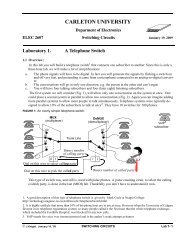
CARLETON UNIVERSITY<br />
Deparment <strong>of</strong> <strong>Electronics</strong><br />
ELEC 2607 Switching Circuits March 1, ’06<br />
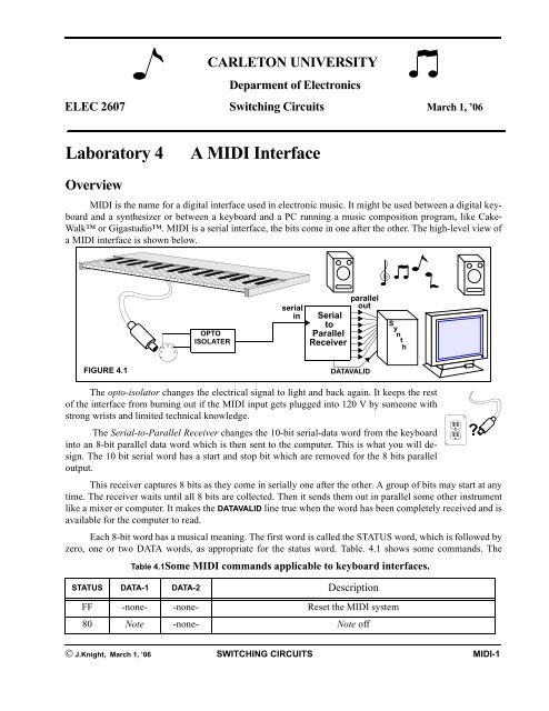
<strong>Labor<strong>at</strong>ory</strong> 4 A <strong>MIDI</strong> <strong>Interface</strong><br />
Overview<br />
<strong>MIDI</strong> is the name for a digital interface used in electronic music. It might be used between a digital keyboard<br />
and a synthesizer or between a keyboard and a PC running a music composition program, like Cake-<br />
Walk or Gigastudio. <strong>MIDI</strong> is a serial interface, the bits come in one after the other. The high-level view <strong>of</strong><br />
a <strong>MIDI</strong> interface is shown below.<br />
FIGURE 4.1<br />
OPTO<br />
ISOLATER<br />
serial<br />
in Serial<br />
to<br />
Parallel<br />
Receiver<br />
parallel<br />
out<br />
DATAVALID<br />
The opto-isol<strong>at</strong>or changes the electrical signal to light and back again. It keeps the rest<br />
<strong>of</strong> the interface from burning out if the <strong>MIDI</strong> input gets plugged into 120 V by someone with<br />
strong wrists and limited technical knowledge.<br />
The Serial-to-Parallel Receiver changes the 10-bit serial-d<strong>at</strong>a word from the keyboard ?<br />
into an 8-bit parallel d<strong>at</strong>a word which is then sent to the computer. This is wh<strong>at</strong> you will design.<br />
The 10 bit serial word has a start and stop bit which are removed for the 8 bits parallel<br />
output.<br />
This receiver captures 8 bits as they come in serially one after the other. A group <strong>of</strong> bits may start <strong>at</strong> any<br />
time. The receiver waits until all 8 bits are collected. Then it sends them out in parallel some other instrument<br />
like a mixer or computer. It makes the DATAVALID line true when the word has been completely received and is<br />
available for the computer to read.<br />
Each 8-bit word has a musical meaning. The first word is called the STATUS word, which is followed by<br />
zero, one or two DATA words, as appropri<strong>at</strong>e for the st<strong>at</strong>us word. Table. 4.1 shows some commands. The<br />
Table 4.1Some <strong>MIDI</strong> commands applicable to keyboard interfaces.<br />
STATUS DATA-1 DATA-2 Description<br />
FF -none- -none- Reset the <strong>MIDI</strong> system<br />
80 Note -none- Note <strong>of</strong>f<br />
© J.Knight, March 1, ’06 SWITCHING CIRCUITS <strong>MIDI</strong>-1<br />
S ynth
<strong>Carleton</strong> University Overview<br />
words STATUS, DATA-1 and DATA-2 are interpreted in s<strong>of</strong>tware. If you are interested in interpreting <strong>MIDI</strong><br />
commands you might try to continue this work as a final-year project. This lab will look only <strong>at</strong> the hardware<br />
part <strong>of</strong> the interface.<br />
The Serial Signal<br />
Table 4.1Some <strong>MIDI</strong> commands applicable to keyboard interfaces.<br />
STATUS DATA-1 DATA-2 Description<br />
90 Note Velocity Turn on Note in DATA-1 with key Velocity in DATA-2<br />
D0 Pressure -none- Change key pressure <strong>of</strong> the current note, in mid-note.<br />
The keyboard will send out a word made up <strong>of</strong> 10 bits sent serially one after the other. The idle time between<br />
words is <strong>of</strong> indefinite length.<br />
FIGURE 4.2 A typical <strong>MIDI</strong> signal showing three words.<br />
FIGURE 4.3 The protocol used by <strong>MIDI</strong> equipment. The d<strong>at</strong>a bits are drawn as both 1 and 0 since they<br />
may be either.<br />
IDLE<br />
10 BIT WORD<br />
INDEFINITE<br />
IDLE<br />
TIME<br />
10 BIT WORD<br />
10 BIT WORD<br />
START<br />
BIT<br />
LEAST<br />
SIGNIFC<br />
BIT<br />
32.0 µs<br />
0.320 ms<br />
8 DATA BITS<br />
MOST<br />
SIGNIFC<br />
BIT<br />
IDLE: The signal is always “1” when idle.<br />
START BIT: The signal always has one low (0) bit before the 8 d<strong>at</strong>a bits start. This tells the interface to<br />
start listening.<br />
DATA BITS: 8 d<strong>at</strong>a bits follow the start bit. Any individual bit may be “1” or “0.” Table. 4.1, shows<br />
STATUS words always start with a “1”, DATA -1 and DATA-2 words always start with a “0.”<br />
STOP BIT: The STOP BIT follows the last d<strong>at</strong>a bit and is always “1”. It is really the start <strong>of</strong> the next<br />
idle period. The next start bit may come immedi<strong>at</strong>ely after the stop bit, or the signal may be<br />
idle for years.<br />
Sampling the Individual Serial Bits<br />
Each bit is transmitted for 32.0 µs. Your circuit will sample each bit in the<br />
<strong>MIDI</strong> signal with a SAMPLE signal which will have a 4.0 µs period.The <strong>MIDI</strong> signal<br />
will be sampled during the 4.0µs th<strong>at</strong> SAMPLE is high.<br />
One would like to sample the <strong>MIDI</strong> signal in the middle <strong>of</strong> each bit where the<br />
d<strong>at</strong>a is stable. This does not happen n<strong>at</strong>urally. You must design your circuit so the<br />
downward edge <strong>of</strong> the start bit starts the SAMPLE signal. However SAMPLE stays<br />
IDLE TIME WAS ZERO HERE<br />
<strong>MIDI</strong>-2 SWITCHING CIRCUITS © J.Knight, March 1, ’06<br />
STOP<br />
BIT<br />
INDEFINITE<br />
IDLE<br />
TIME<br />
32.0 µs<br />
SAMPLE<br />
IDLE<br />
time<br />
NEXT<br />
START<br />
BIT<br />
4.0 µs<br />
time
low for ~14µs so th<strong>at</strong> its high part will come near the centre <strong>of</strong> the <strong>MIDI</strong> bit. Sample will then go high for 4.0µs<br />
during which time the <strong>MIDI</strong> signal is sampled. Then SAMPLE goes low for 28µs and comes up again in the<br />
middle <strong>of</strong> the next <strong>MIDI</strong> bit. SAMPLE is periodic so all ten bits will also be sampled near their middles. Then<br />
SAMPLE goes low and waits for the next START BIT.<br />
FIGURE 4.4 The detailed timing rel<strong>at</strong>ions between the <strong>MIDI</strong> signal and the SAMPLE signal.<br />
~14.0µs<br />
Idle period<br />
Start <strong>of</strong><br />
10-bit<br />
<strong>MIDI</strong> word<br />
FIGURE 4.5 This shows the falling edge <strong>of</strong> the START bit (<strong>at</strong> the big black down-arrow) for three consecutive<br />
Midi instructions. Approxim<strong>at</strong>ely 14µs after this edge (3 or 4 clock-cycles) , the SAMPLE signal<br />
starts. It then goes on and samples all 10 bits near the middle where they are stable. After 10 bits<br />
SAMPLE goes low and stays low until restarted by the next START bit.<br />
SAMPLE<br />
<strong>MIDI</strong> SIGNAL<br />
32.0µs<br />
32.0µs<br />
4.0µs<br />
Design Problem for This Lab<br />
28.0µs<br />
SAMPLE<br />
<strong>MIDI</strong> SIGNAL<br />
In this lab, you will design the logical part <strong>of</strong> the <strong>MIDI</strong> interface, the serial-to-parallel receiver. You will<br />
draw your circuit on the screen, simul<strong>at</strong>e the results, and download it to a complex logic device (CPLD).<br />
The Receiver<br />
Signals which are restricted so they physically cannot change <strong>at</strong> the same time as the active clock edge<br />
are called synchronous. If they might be able to change on th<strong>at</strong> clock edge, they are called asynchronous.<br />
The receiver input is called asynchronous because the start <strong>of</strong> a new word (the start <strong>of</strong> the START BIT)<br />
<strong>at</strong> the <strong>MIDI</strong> input (SI) does not have a known rel<strong>at</strong>ionship with the receiver clock. Each new word in the SI signal<br />
may start <strong>at</strong> a random or asynchronous time.<br />
FIGURE 4.6 Diagram showing receiver inputs and outputs<br />
<strong>MIDI</strong> input<br />
SI<br />
CLK<br />
4.0µs period<br />
RST<br />
DATA0<br />
DATA1<br />
DATA2<br />
DATA3<br />
The receiver has the following input and output signals<br />
32<br />
32<br />
SERIAL-TO PARALLEL<br />
RECEIVER<br />
FOR AN<br />
ASYNCHRONOUS INPUT<br />
DATA4<br />
Idle period<br />
End <strong>of</strong><br />
10-bit<br />
<strong>MIDI</strong> word<br />
© J.Knight,March 1, ’06 SWITCHING CIRCUITS <strong>MIDI</strong>-3<br />
DATA5<br />
DATA6<br />
DATA7<br />
DATA-VALID<br />
most significant bit
<strong>Carleton</strong> University For The Prelab, Implement This Design<br />
SI Serial Input.....The received <strong>MIDI</strong> signal<br />
CLK This is supplied externally, say from a PC, and has a period <strong>of</strong> 4.0 µs, 8 times the signal bit<br />
speed. CLK is not synchronized with SI. The rising/falling edges <strong>of</strong> CLK are <strong>at</strong> arbitrary<br />
times with respect to the rising/falling edges <strong>of</strong> SI.<br />
The CLK is sacred. It must go to the clock pin <strong>of</strong> all counters and flip-flops. It must not go<br />
through g<strong>at</strong>es or be delayed in any way. All flip-flops must clock <strong>at</strong> the same time. If the<br />
clock reaches them <strong>at</strong> different times it is called clock skew, which causes many problems<br />
RST Asynchronous reset; this is used for initializing the circuit on power-up. It is also used in<br />
factories for autom<strong>at</strong>ic testing. It should go to the CLR connection 1 on every flip-flop. It<br />
must not be used for things like clearing a counter <strong>at</strong> the end <strong>of</strong> its count.<br />
DATA0...DATA7 The received 8-bit d<strong>at</strong>a word. DATA0 is the least significant bit.<br />
DATAVALID DATAVALID = 0 whenever the d<strong>at</strong>a on the parallel output pins may not represent the last serial<br />
word received, th<strong>at</strong> is the last word may be corrupted by new incoming d<strong>at</strong>a.<br />
DATAVALID = 1 after the STOP BIT has been received, and the d<strong>at</strong>a may be read out in parallel<br />
by the computer. It stays 1 until new serial input d<strong>at</strong>a changes the parallel output lines.<br />
For The Prelab, Implement This Design<br />
Modular Design<br />
The interface can be divided into modules such as shown on the next page. We strongly encourage you to<br />
use modular design. Enter and test each part individually.<br />
Suggested modules and their input and output signals are shown. If you use these modules and the same<br />
wire names, you can use the test input files supplied.<br />
SI<br />
CLK<br />
ACTIVE<br />
SAMPLE<br />
DATAVALID<br />
QUIT<br />
Waveforms<br />
Consider the signals shown above. Also refer to the block diagram Fig. 4.7. The CLK goes to all flipflops<br />
all the time. The SAMPLE signal enables certain flip-flops to effectively clock <strong>at</strong> a slower r<strong>at</strong>e without<br />
causing clock skew. Placing a g<strong>at</strong>e in the clock line could also do this, but this would cause clock skew and<br />
false clock edges, horrors which you will learn about in ELEC 3500.<br />
1. Xilinx library flip-flops use CLR for asynchronous reset and R for synchronous reset.<br />
FIGURE 4.8<br />
<strong>MIDI</strong>-4 SWITCHING CIRCUITS © J.Knight, March 1, ’06
SI<br />
Serial In<br />
RST<br />
CLK<br />
The flip-flops inside the CONTROL and SER2PAR blocks change only when enabled by SAMPLE.<br />
Signals in STRT_STP and DIVBY8 respond <strong>at</strong> the 40 µs clock r<strong>at</strong>e.<br />
The ACTIVE signal<br />
DATAVALID (goes high on the 1st SAMPLE pulse, and goes low after 10)<br />
STRT_STP<br />
DIVBY8<br />
ACTIVE SAMPLE<br />
RST<br />
QUIT<br />
SAMPLE<br />
SI<br />
SER2PAR<br />
RST<br />
DATAVALID<br />
ACTIVE goes high after the START BIT in SI goes low. It stays high until after half way through the<br />
STOP BIT. Thus ACTIVE tells when there is a serial signal coming in.<br />
ACTIVE going high starts the DIVBY8 counter. This counts 4 CLK cycles and then sends out the SAM-<br />
PLE pulse.The sample pulse is one clock-cycle wide in the middle <strong>of</strong> each bit <strong>of</strong> SI. SAMPLE always comes in<br />
the middle <strong>of</strong> each bit where SI is stable. Not <strong>at</strong> the edges where SI is changing.<br />
The DATAVALID signal<br />
DATAVALID is fed back from the CONTROL block into STRT_STP to turn <strong>of</strong>f ACTIVE <strong>at</strong> the end <strong>of</strong><br />
each 10 bit word.<br />
To initially lower DATAVALID when a word starts to be received, use the first SAMPLE pulse.<br />
The SAMPLE pulses start 4 clk cycles after ACTIVE goes true.<br />
After sending out the first SAMPLE pulse, the DIVBY8 counter now counts 8 clock cycles and sends out another<br />
SAMPLE pulse. The DIVBY8 counter continues as long as ACTIVE is true.<br />
The CONTROL block counts the number <strong>of</strong> bits:<br />
It knows the last d<strong>at</strong>a bit is sampled, after 9 SAMPLE pulses (the counter reads 9).<br />
It knows the STOP BIT is sampled, after 10 SAMPLE pulses (the counter reads 0).<br />
After DATAVALID becomes true, the ACTIVE signal is turned <strong>of</strong>f.<br />
The QUIT signal<br />
After 9 SAMPLE pulses the QUIT signal tells the SER2PAR block th<strong>at</strong> all the d<strong>at</strong>a-bits are read, and it<br />
should stop collecting d<strong>at</strong>a. Note the difference between all the d<strong>at</strong>a-bits, and all the d<strong>at</strong>a-bits plus the stop bit.<br />
© J.Knight,March 1, ’06 SWITCHING CIRCUITS <strong>MIDI</strong>-5<br />
RST<br />
DATA0<br />
DATA1<br />
DATA2<br />
DATA3<br />
DATA4<br />
DATA5<br />
DATA6<br />
DATA7<br />
CONTROL<br />
QUIT<br />
QUIT receiving new d<strong>at</strong>a, only the STOP or idle bits are coming in.<br />
DATAVALID<br />
Read the 8 DATAx lines<br />
only if DATAVALID=1.<br />
FIGURE 4.7 Block diagram showing suggested block names and wire (net) names for the <strong>MIDI</strong><br />
interface.You may have to make minor modific<strong>at</strong>ions to this, or to the preloaded file.
<strong>Carleton</strong> University Description <strong>of</strong> the Blocks<br />
Description <strong>of</strong> the Blocks<br />
The STRT_STP Block<br />
Refer to the timing diagram Fig. 4.9. Note particularly:<br />
Region B is shaded .<br />
Region C is shaded .<br />
Note the values <strong>of</strong> SI, DATAVALID and ACTIVE in the regions A, B, and C.<br />
Region C is when SI is not active, th<strong>at</strong> is idle. See Fig. 4.4.<br />
When Region A is where ACTIVE starts up, but before DATAVALID goes false (low).<br />
Design the circuit to gener<strong>at</strong>e the ACTIVE signal from SI and DATAVALID.<br />
FIGURE 4.9 Timing used to gener<strong>at</strong>e the circuit for STRT_STP<br />
SI<br />
DATAVALID<br />
0<br />
1<br />
0<br />
ACTIVE<br />
B<br />
C<br />
A<br />
Complete truth table, Karnaugh map and schem<strong>at</strong>ic for STRT_STP. With proper use <strong>of</strong> don’t cares, you will<br />
need only one 2-input g<strong>at</strong>e. Don’t cares come from impossible inputs; why cannot DATAVALID stay 0 in region<br />
C?<br />
DIVBY8<br />
This circuit basically divides the clock by 8 to get a 32.0µs time base, which is used to gener<strong>at</strong>e a single<br />
4µs pulse every 32.0µs..<br />
ACTIVE<br />
CE<br />
CLK<br />
RST<br />
Q0<br />
Q1<br />
Q2<br />
to where?<br />
CLR = ASYNCHRONOUS RESET<br />
CE = CHIP INPUT ENABLE<br />
CARRY OUT “TC” ON 7 COUNT<br />
Care must be taken to only sample the SI signal when it is stable. One way is to read SI in the middle <strong>of</strong><br />
each bit. Since CLK is 8 times the bit r<strong>at</strong>e <strong>of</strong> SI, this can be done sampling the first bit after 4 CLK pulses and<br />
<strong>MIDI</strong>-6 SWITCHING CIRCUITS © J.Knight, March 1, ’06<br />
D<br />
C<br />
CE<br />
D<br />
C<br />
CE<br />
D<br />
C<br />
CE<br />
Q<br />
CLR<br />
Q<br />
CLR<br />
Q<br />
CLR<br />
TC<br />
Q0<br />
Q1<br />
Q2<br />
stop<br />
bit<br />
Q0 + = ( Q0 )·CE + Q0·CE<br />
On the flip-flops<br />
CE = Clock Enable (Chip Enable)<br />
The Q output will not change unless<br />
CE is high.<br />
1<br />
1<br />
FIGURE 4.10<br />
A 3-bit binary counter you<br />
will need to modify<br />
Q1 + =( Q0⊕Q1)·CE + Q1·CE<br />
fdce in the Xilinx libraries<br />
Use fdc if CE is not needed.<br />
Q2 + = (Q2⊕(Q1·Q0)·CE + Q2·CE<br />
Where should ACTIVE be placed in these<br />
equ<strong>at</strong>ions?
then every 8 pulses thereafter. A counter which counts up to 8, can do the proper frequency division.<br />
The most significant bit Q2 will change <strong>at</strong> 1/8 <strong>of</strong> the clock frequency.<br />
A typical binary counters is shown in Fig. 4.10. This counter has an output called TC (terminal count). It<br />
gives a pulse, one clock cycle wide, every 8 clock cycles (every count <strong>of</strong> 7). TC was designed to trigger another<br />
counter to allow the two counters to count to 64. If you are counting every clock cycle you do not need CE.<br />
The circuit shown can be modified to give an output after 4 clock cycles (a count <strong>of</strong> 3) and every 8 cycles<br />
thereafter. It should also be modified so the count goes to zero when ACTIVE goes low. This should be done<br />
synchronously, on a clock edge, by feeding zeros to the D inputs. Don’t even think about using the asynchronous<br />
CLR for this. This counter is a starting point for DIVBY8, but some <strong>of</strong> the names and circuitry are different.<br />
For example TC and GoToZero will need to be changed. It may help to look <strong>at</strong> the st<strong>at</strong>e graph on p.10.<br />
The CONTROL Block<br />
This circuit counts the SAMPLE pulses and gener<strong>at</strong>es two signals from the count:<br />
1) The QUIT signal tells the serial-to-parallel shift-register th<strong>at</strong> all the d<strong>at</strong>a-bits are read, and it should stop<br />
shifting. Note there is a difference between all the d<strong>at</strong>a-bits, and all the d<strong>at</strong>a-bits plus the stop bit.<br />
2) The DATAVALID signal turns <strong>of</strong>f ACTIVE.<br />
DATAVALID must be 1 <strong>at</strong> the very start <strong>of</strong> the START-BIT in SI to initi<strong>at</strong>e raising the ACTIVE signal.<br />
This circuit needs to count 10 sample pulses, start, 8 d<strong>at</strong>a bits and stop. This is a decimal counter. Such a<br />
counter has Q0, Q1 and Q2 exactly like the previous binary counter. However Q3 must be added. Note the st<strong>at</strong>e<br />
after nine is not ten, but zero. If you have designed the previous counter to synchronously go to zero on a count<br />
<strong>of</strong> three, then you know how to make this counter go to zero synchronously after a count <strong>of</strong> nine.<br />
Note the counter chip enable (CE) holds the counter <strong>at</strong> its old count until enabled by SAMPLE. Hence use<br />
flip-flops with chip-enable (Xilinx cell fdce) in this design.<br />
Altern<strong>at</strong>e CONTROL Block<br />
One does not need to design a separ<strong>at</strong>e counter. The shift register described in the SER2PAR block can<br />
keep track <strong>of</strong> the number <strong>of</strong> bits coming in. Use an extra D flip-flop and a g<strong>at</strong>e to clear or set every flip-flop on<br />
the 11th SAMPLE pulse.You must be able to tell when the input SI has finished, no m<strong>at</strong>ter wh<strong>at</strong> the d<strong>at</strong>a is.<br />
RST<br />
CLK<br />
SI<br />
DATAVALID<br />
STRT_STP<br />
FIGURE 4.11<br />
The SER2PAR Block<br />
You need to design an 8-bit serial-in/parallel-out<br />
shift register in which you can serially<br />
shift in the d<strong>at</strong>a bit values as they are read. Run<br />
the flip-flops from the 4ms clock, but use the<br />
CE (chip enable) inputs so they are effectively<br />
DIVBY8<br />
ACTIVE SAMPLE<br />
RST<br />
DATA0<br />
DATA1<br />
DATA2<br />
DATA3<br />
DATA4<br />
DATA5<br />
DATA6<br />
DATA7<br />
© J.Knight,March 1, ’06 SWITCHING CIRCUITS <strong>MIDI</strong>-7<br />
SI<br />
DATAVALID<br />
SER2PAR2<br />
DATA0 should be the 1st bit after START<br />
RST<br />
D<br />
C<br />
CLR<br />
Q=d<strong>at</strong>a4<br />
D<br />
C<br />
CLR<br />
Q=D<strong>at</strong>a3<br />
D<br />
C<br />
CLR<br />
Q-D<strong>at</strong>a2<br />
D<br />
C<br />
CLR<br />
DATAVALID<br />
Q=D<strong>at</strong>a1<br />
D<br />
C<br />
CLR<br />
Q=D<strong>at</strong>a0
<strong>Carleton</strong> University In The Lab.<br />
clocked <strong>at</strong> the SAMPLE r<strong>at</strong>e. A basic shift register shifts all bits right one flip flop every clock cycle, and is illustr<strong>at</strong>ed.<br />
It does not use the CE, but you should.<br />
In The Lab.<br />
After you have designed the circuit, you will enter it graphically into the<br />
computer as schem<strong>at</strong>ic diagrams. Instructions for doing this will be given in the<br />
labor<strong>at</strong>ory. After the circuit is entered, you will simul<strong>at</strong>e it to check its oper<strong>at</strong>ion.<br />
While the blocks are individually simple, connecting the whole circuit <strong>at</strong><br />
once will make debugging difficult. Implement the above blocks one <strong>at</strong> a time.<br />
Test fixture files are available to help you simul<strong>at</strong>e the individual blocks. There is<br />
also a test file to simul<strong>at</strong>e the whole <strong>MIDI</strong> interface.<br />
By the end <strong>of</strong> the first lab period you should aim to have entered three <strong>of</strong><br />
the blocks. Simul<strong>at</strong>ing and debugging will be slow. Do not leave too much for<br />
the second period.<br />
Displaying Waveforms<br />
The test fixture file can do a lot to help you check your circuit. There are<br />
three waveforms, not in your circuit, which should be displayed.<br />
StudNumb displays your student number for comparison with the midi d<strong>at</strong>a.<br />
startguide displays a pulse during the start bit to make it easy to find.<br />
serialin displays the serial input d<strong>at</strong>a as an integer.<br />
d<strong>at</strong>a displays the parallel output d<strong>at</strong>a as an integer, with DATA0 as the least<br />
significant bit.<br />
The Test for the Complete Circuit<br />
After you have run the simul<strong>at</strong>ion file on the full <strong>MIDI</strong> schem<strong>at</strong>ic, you should run it with your own d<strong>at</strong>a.<br />
The test files are written in Verilog, a language for describing and simul<strong>at</strong>ing digital circuits. You will<br />
use Verilog next year in ELEC3500.<br />
All Verilog instructions end in semicolons. If there is no “;” the instruction is continued on the next line.<br />
Comments start with //.<br />
In the midi file, the 10 values <strong>of</strong> SI which make up the <strong>MIDI</strong> word are written out serially<br />
as in Fig. 4.12 The values <strong>of</strong> SI are set. The #32 indic<strong>at</strong>es a 32 µs delay before the next<br />
change. Thus both boxes on the right give the pulse shown below them. Writing the #32 between<br />
the lines makes it clearer where the delay is, but takes more space.<br />
The d<strong>at</strong>a word shown Fig. 4.12 is 0 0 1 1 0 0 0 1 1 1, the start and stop bits are underlined.<br />
// Start bit<br />
SI=0; startguide=1;<br />
#32; startguide=0;<br />
// 8 D<strong>at</strong>a bits<br />
SI=0;<br />
#32;<br />
SI=1;<br />
#32;<br />
SI=1;<br />
#32;<br />
SI=0;<br />
#32;<br />
SI=0;<br />
#32;<br />
SI=0;<br />
#32;<br />
SI=1;<br />
#32;<br />
SI=1;<br />
#32;<br />
// Stop Bit<br />
SI=1;<br />
#90;<br />
Your student number, or your partners, is used as d<strong>at</strong>a in the midi test_top.tf test fixture file.<br />
integer StudNumb;<br />
// ENTER YOUR STUDENT NUMBER HERE.<br />
//------------------------------initial<br />
StudNumb = 312153;<br />
//-------------------------------<br />
The Verilog program will transl<strong>at</strong>e it into binary, and use the 8 least significant bits as test d<strong>at</strong>a.<br />
FIGURE 4.12<br />
Part <strong>of</strong> the test file<br />
SI = 0;<br />
#32;<br />
SI = 1;<br />
#32;<br />
SI = 0;<br />
SI = 0;<br />
#32 SI = 1;<br />
#32 SI=0<br />
<strong>MIDI</strong>-8 SWITCHING CIRCUITS © J.Knight, March 1, ’06<br />
SI<br />
32 64
SI<br />
CLK<br />
In the simul<strong>at</strong>ion the incoming midi bits are exactly 32µs long and the receiver clock is exactly 4µs. Normally<br />
the transmitters idea <strong>of</strong> a µs is not the same as the receivers.One will be a little faster. If the clock period<br />
were say 2.4 µs the SAMPLE pulse would not be in the right place to sample the final bits.<br />
Changes to the midi test_top.tf (test_top2.tf) file<br />
ACTIVE<br />
SAMPLE<br />
SI<br />
CLK<br />
ACTIVE<br />
1) Change the part <strong>of</strong> the file shown in Fig. 4.12 to make the d<strong>at</strong>a word to 0110011001<br />
2) Make sure the signal StudNumb is on your list <strong>of</strong> signals to be displayed.<br />
Run the simul<strong>at</strong>ion with the default StudNumb=312153.<br />
Then enter your student number in midi_test and rerun the simul<strong>at</strong>ion. 2<br />
3) (Optional) Making the interface fail<br />
Find, in test_top.tf, where the clock is gener<strong>at</strong>ed and change the period to 4.1µs. Note the delay is a<br />
half period. If you reduce the clock speed, the SAMPLE pluses will be further apart, but the SI bits will<br />
come in <strong>at</strong> the same r<strong>at</strong>e. Their speed is controlled by a different clock.<br />
SAMPLE<br />
Increase the delay in 0.1µs steps until you lose the final d<strong>at</strong>a bit. The timescale in the program will not<br />
accept any finer resolution than 0.1µs.<br />
The test fixture has been set up to print, in the log file, the serial-in parallel-out values for the d<strong>at</strong>a, albeit<br />
in hexadecimal. It is easy to see if they are not the same.<br />
Your Report<br />
The marker will not believe th<strong>at</strong> you intuitively know how the Midi interface works. You must explain,<br />
<strong>at</strong> a high level, the function <strong>of</strong> the complete interface and the individual blocks. For example, could you not<br />
give a better explain<strong>at</strong>ion <strong>of</strong> the ser2par block than is in the lab sheet.<br />
Your design and design methods should be included. Most peoples designs will follow the prelab outline.<br />
Brag about any changes you made, particularly if you think they are an improvement.<br />
Your report should be coherent, and not jump over design deriv<strong>at</strong>ions. Put in your schem<strong>at</strong>ics and your<br />
final simul<strong>at</strong>ion. The circuits should agree with those you actually used.<br />
2. If 312153 is your student number, use your lab partners number.<br />
FIGURE 4.13showing<br />
where the d<strong>at</strong>a bits<br />
are sampled<br />
FIGURE 4.14 With a<br />
slower clock, the<br />
last bit is skipped.<br />
© J.Knight,March 1, ’06 SWITCHING CIRCUITS <strong>MIDI</strong>-9
<strong>Carleton</strong> University Your Report<br />
Testing and implement<strong>at</strong>ion are important. You should ne<strong>at</strong>ly highlight and write comments on the<br />
waveforms. It is very hard for someone to make sense <strong>of</strong> simul<strong>at</strong>ion waveforms if they do not know wh<strong>at</strong> is being<br />
simul<strong>at</strong>ed. You must explain wh<strong>at</strong> the waveforms mean.<br />
Common reasons for losing marks in <strong>MIDI</strong> reports<br />
The author <strong>of</strong> each section is not identified <strong>at</strong> the top <strong>of</strong> each section.<br />
The report uses two much unexplained jargon. For a reference level, assume your report will be used a<br />
crutch for a student doing the lab next year. He/she should be able to understand it.<br />
The paragraphs or sentences do not make sense. Example from a recent report, “Since SI is asynchronous,<br />
the SI d<strong>at</strong>a is input when the d<strong>at</strong>a is low.”<br />
Not describing the modific<strong>at</strong>ions th<strong>at</strong> had to be done to modules.<br />
Not describing the final simul<strong>at</strong>ion. This is the test th<strong>at</strong> your circuit works. St<strong>at</strong>e how you know your circuit<br />
works. Be sure to write short ne<strong>at</strong> comments on the waveform printout.<br />
We repe<strong>at</strong>! Annot<strong>at</strong>e your waveforms.<br />
Leaving out sections.<br />
Copying the sections verb<strong>at</strong>im from the labor<strong>at</strong>ory write-up.<br />
Copying pictures from the lab sheet and not acknowledging them.<br />
Not <strong>at</strong>taching the prelab as an appendix.<br />
Not placing your names on the schem<strong>at</strong>ics.<br />
Copying a last years report. The changes give this away easily. Plagiarism is a major <strong>of</strong>fense.<br />
FIGURE 4.15 St<strong>at</strong>e graphs for DIVBY8 and CONTROL<br />
6<br />
7<br />
5<br />
0<br />
ACTIVE<br />
4<br />
1<br />
2<br />
3<br />
sample<br />
9<br />
QUIT<br />
<strong>MIDI</strong>-10 SWITCHING CIRCUITS © J.Knight, March 1, ’06<br />
s<br />
8<br />
s<br />
7<br />
s<br />
s<br />
6<br />
0<br />
QUIT<br />
D<strong>at</strong>aValid<br />
s<br />
5<br />
s<br />
s = sample<br />
4<br />
1<br />
2<br />
3<br />
s<br />
s<br />
s