Growth of Intermetallic Compounds in Thermosonic Copper Wire ...
Growth of Intermetallic Compounds in Thermosonic Copper Wire ...
Growth of Intermetallic Compounds in Thermosonic Copper Wire ...
You also want an ePaper? Increase the reach of your titles
YUMPU automatically turns print PDFs into web optimized ePapers that Google loves.
<strong>Growth</strong> <strong>of</strong> <strong>Intermetallic</strong> <strong>Compounds</strong> <strong>in</strong> <strong>Thermosonic</strong> <strong>Copper</strong> <strong>Wire</strong> Bond<strong>in</strong>g on Alum<strong>in</strong>um Metallization 125<br />
bonds <strong>in</strong> the as-bonded state. 12,13 Studies by Kim<br />
et al. showed that the growth rate <strong>of</strong> Cu-Al IMCs<br />
between the copper and Al-1% Si-0.5% Cu metallization<br />
was approximately 1/10 <strong>of</strong> that for Au-Al<br />
IMCs <strong>in</strong> the temperature range <strong>of</strong> 150°C to 300°C. 14<br />
The atomic properties <strong>of</strong> the elements (i.e., copper,<br />
gold, and alum<strong>in</strong>um) could be used to expla<strong>in</strong> the<br />
large difference <strong>in</strong> the growth rates <strong>of</strong> IMCs. Compared<br />
with an atom <strong>of</strong> Au, an atom <strong>of</strong> Cu has a<br />
larger size misfit with alum<strong>in</strong>um and lower electronegativity,<br />
thus mak<strong>in</strong>g the formation <strong>of</strong> Cu-Al<br />
IMCs much more difficult than the formation <strong>of</strong><br />
Au-Al IMCs. 13 However, the k<strong>in</strong>etics <strong>of</strong> Cu-Al IMCs,<br />
<strong>in</strong>clud<strong>in</strong>g their activation energy, <strong>in</strong> thermosonic<br />
Cu-Al bonds was not clearly documented, although<br />
there were some studies on bulk and th<strong>in</strong>-film Cu-Al<br />
couples. 15–19<br />
Different IMCs can be formed at the <strong>in</strong>terface and<br />
affect the reliability <strong>of</strong> bonds. IMCs with high melt<strong>in</strong>g<br />
po<strong>in</strong>ts (e.g., above 1000°C) are stable at <strong>in</strong>terfaces<br />
and should not significantly affect reliability. IMCs<br />
with low melt<strong>in</strong>g po<strong>in</strong>ts (e.g., below 500°C) are less<br />
stable and their constituents will cont<strong>in</strong>ue to diffuse,<br />
which can affect reliability. Accord<strong>in</strong>g to<br />
the b<strong>in</strong>ary phase diagram <strong>of</strong> the Cu-Al system,<br />
five IMCs—CuAl2 (h phase), CuAl (g2 phase), Cu4Al3<br />
(f2 phase), Cu3Al2 (d phase), and Cu9Al4 (c2 phase)—<br />
can exist at temperatures below 300°C.<br />
Previously, studies <strong>of</strong> the <strong>in</strong>terfacial behavior <strong>of</strong><br />
Cu-Al bonds were mostly carried out us<strong>in</strong>g optical<br />
microscopy (OM) and SEM with an energy-dispersive<br />
x-ray spectrometer (EDX). 10–13<br />
It should be<br />
noted that these techniques are not able to provide<br />
detailed <strong>in</strong>formation on crystallographic structure,<br />
therefore the expected <strong>in</strong>termetallic phases <strong>in</strong> Cu-Al<br />
bonds were not clearly identified. Transmission<br />
electron microscopy (TEM) is able to analyze the<br />
Cu-Al bond <strong>in</strong>terface on the nanoscale and identify<br />
its crystallographic structure. The ma<strong>in</strong> challenge<br />
for TEM analysis <strong>of</strong> a wire bond is associated with<br />
specimen preparation s<strong>in</strong>ce region-specific analysis<br />
is necessary. In addition, conventional specimen<br />
preparation can result <strong>in</strong> mechanical damage <strong>of</strong> the<br />
<strong>in</strong>terface region dur<strong>in</strong>g polish<strong>in</strong>g. These problems<br />
can be overcome by us<strong>in</strong>g a dual-beam focused ion<br />
beam (FIB) system, which comb<strong>in</strong>es SEM with a<br />
scann<strong>in</strong>g ion beam. In this way specific regions can<br />
be located us<strong>in</strong>g SEM, and TEM specimen prepared<br />
without the application <strong>of</strong> mechanical forces.<br />
In this paper, we report the <strong>in</strong>terfacial morphology<br />
<strong>of</strong> copper bonds on alum<strong>in</strong>um metallization <strong>in</strong><br />
the as-bonded state, followed by the growth characteristics<br />
<strong>of</strong> Cu-Al IMCs at high temperatures and<br />
extended ag<strong>in</strong>g times. The growth k<strong>in</strong>etics <strong>of</strong> Cu-Al<br />
IMCs is exam<strong>in</strong>ed as well as the effect <strong>of</strong> ag<strong>in</strong>g<br />
temperature and time on the morphology <strong>of</strong> IMCs.<br />
F<strong>in</strong>ally, the <strong>in</strong>termetallic compounds <strong>in</strong> the bonds<br />
are identified by selected-area electron diffraction<br />
(SAD) on specimens prepared by a dual-beam FIB<br />
system. We also attempt to elucidate the mechanism<br />
<strong>of</strong> <strong>in</strong>terfacial reaction between the copper wire<br />
and alum<strong>in</strong>um metallization dur<strong>in</strong>g the bond<strong>in</strong>g<br />
process and thermal ag<strong>in</strong>g.<br />
EXPERIMENTAL PROCEDURES<br />
In our experimental studies, a copper wire<br />
(99.99 wt.%) with a diameter <strong>of</strong> 50.8 lm was bonded<br />
to a 3-lm-thick Al metallization pad on a silicon<br />
chip us<strong>in</strong>g an ASM Eagle 60 ball/wedge automatic<br />
bonder with an ultrasonic frequency <strong>of</strong> 138 kHz. An<br />
electronic flame-<strong>of</strong>f (EFO) process was applied to<br />
produce a spherical ball at the end <strong>of</strong> copper wire as<br />
the first step <strong>of</strong> the bond<strong>in</strong>g cycle. The <strong>in</strong>itial copper<br />
ball was achieved with a current <strong>of</strong> 150 mA and a<br />
gap voltage <strong>of</strong> 5500 V with a discharge time <strong>of</strong><br />
1.3 ms. In order to prevent the copper ball from<br />
oxidiz<strong>in</strong>g <strong>in</strong> the EFO process, a protective shield<strong>in</strong>g<br />
gas—95% N2 +5% H2—was supplied and ma<strong>in</strong>ta<strong>in</strong>ed<br />
at a flow rate <strong>of</strong> 0.8 L/m<strong>in</strong>. The copper ball<br />
was then bonded to alum<strong>in</strong>um metallization us<strong>in</strong>g a<br />
comb<strong>in</strong>ation <strong>of</strong> heat, transverse ultrasonic vibration,<br />
and normal force. The detailed bond<strong>in</strong>g<br />
parameters are shown <strong>in</strong> Table I for the process<br />
w<strong>in</strong>dow optimized by means <strong>of</strong> pull/shear tests and<br />
dimension tests.<br />
In order to accelerate <strong>in</strong>terfacial evolution and<br />
ascerta<strong>in</strong> the growth k<strong>in</strong>etics <strong>of</strong> Cu-Al IMCs, samples<br />
were thermally aged at 200°C for up to<br />
121 days, at 250°C for up to 169 h, and at 300°C for<br />
up to 16 h <strong>in</strong> nitrogen.<br />
After thermal ag<strong>in</strong>g, cross-sectional samples were<br />
prepared for SEM observation <strong>of</strong> IMC morphology.<br />
Back-scatter electron (BSE) SEM images were<br />
taken <strong>in</strong> order to highlight the presence <strong>of</strong> different<br />
layers (i.e., Al, Cu-Al IMCs, and Cu). The common<br />
metallographic procedure was performed to reveal<br />
the cross-sectional microstructure: the bonds were<br />
wet-ground with grit size 400, 600, 1000, and 2000<br />
sandpaper, followed by polish<strong>in</strong>g with 1.0-lm and<br />
0.25-lm diamond suspensions on silk cloths. SEM<br />
observations were performed us<strong>in</strong>g a HITACHI<br />
S-4700 system. The average thickness <strong>of</strong> the IMCs<br />
was obta<strong>in</strong>ed for each sample by measur<strong>in</strong>g the<br />
cross-sectional area <strong>of</strong> the layer over a certa<strong>in</strong><br />
length on the SEM image us<strong>in</strong>g an image analyzer.<br />
The microstructure <strong>of</strong> the Cu-Al bonds both <strong>in</strong> the<br />
as-bonded state and after thermal ag<strong>in</strong>g were<br />
<strong>in</strong>vestigated by cross-sectional TEM comb<strong>in</strong>ed with<br />
EDX. The TEM samples were prepared us<strong>in</strong>g FIB<br />
with a lift-out technique. 14 Mo lift-out TEM grids<br />
were used to avoid x-ray energy overlaps with Cu.<br />
TEM analysis was carried out us<strong>in</strong>g the JEOL<br />
2100F system at 200 kV. A microprobe beam <strong>of</strong><br />
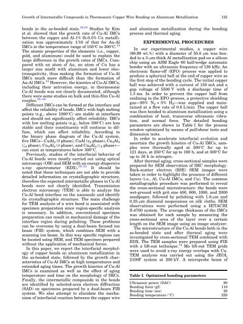
Table I. Optimized bond<strong>in</strong>g parameters<br />
Ultrasonic power (DAC) 90<br />
Bond<strong>in</strong>g force (gf) 110<br />
Bond<strong>in</strong>g time (ms) 28<br />
Bond<strong>in</strong>g temperature (°C) 220


