download
download
download

You also want an ePaper? Increase the reach of your titles
YUMPU automatically turns print PDFs into web optimized ePapers that Google loves.
Report<br />
Evaluating the CAF (conductive anodic filament)<br />
resistance of multi-layered PWBs<br />
Understanding the Technology<br />
New JTM standards for temperature test chambers<br />
– Methods of testing and indicating performance<br />
Topic<br />
New model: Super Clean Oven SCO-2<br />
1<br />
18<br />
29
Evaluating the CAF (conductive anodic filament) resistance of multi-layered PWBs<br />
Report<br />
Evaluating the CAF (conductive anodic filament) resistance of multi-layered PWBs<br />
Akiko Kobayashi, Yuichi Aoki, Keiko Toi Technical Development Headquarters<br />
A<br />
dvances in the high-density wiring of electronic parts have been accompanied<br />
by insulation degradation stemming from ion migration, creating serious<br />
problems. While a great deal of research has been carried out investigating the<br />
formation of dendrites, which are one form of ion migration, there has been a<br />
noticeable lack of clarification of the role of CAF (conductive anodic filament)<br />
formation. As a result, we decided to evaluate the CAF resistance of multi-layered<br />
PWBs (printed wiring boards). We investigated the relationship between the<br />
shape of the CAF that formed and the behavior of insulation resistance levels<br />
during CAF formation. We found that during CAF formation the insulation<br />
resistance levels repeatedly dropped temporarily and then recovered. In addition,<br />
we observed a substance presumed to be CAF at the sites of probable insulation<br />
degradation, and we were able to confirm that this substance occurred along the<br />
glass fibers.<br />
1<br />
Introduction<br />
The electronic components of equipment such as cell phones comprise a great number of<br />
electronic parts embedded onto PWBs. These PWBs normally contain features such as copper<br />
patterns stamped onto the boards and throughholes that penetrate the boards. These lines and<br />
throughholes must have continuous insulation protection from adjacent lines and throughholes.<br />
(Fig.1)<br />
Ion migration, which causes insulation degradation, is a phenomenon in which metallic ions<br />
from the electrodes migrate either on or through the insulation, causing short-circuiting.<br />
Representative types of this phenomenon are dendrites and CAF. (Fig.2)<br />
Fig.1 Enlarged PWB photo<br />
- 1 -<br />
Fig.2 Sites of ion migration<br />
Espec Technology Report No.24
Evaluating the CAF (conductive anodic filament) resistance of multi-layered PWBs<br />
Until recently, measures such as refinements in PWB materials had managed to suppress the<br />
problem of ion migration, but with recent advances producing higher density wiring, ion migration<br />
has once again become a serious problem. In addition, the use of multi-layered circuit boards and<br />
built-in circuit boards has caused the formation of CAF to become an increasingly serious<br />
problem.<br />
CAF is a failure mode in PWBs that occurs under conditions of high humidity and high voltage<br />
gradient. The filament, a copper salt, grows from the anode toward the cathode along the<br />
epoxy/glass interface.<br />
There is a growing trend toward standardization in evaluating CAF resistance, and in 2003, the<br />
IPC Association Connecting Electronics Industries issued standards for the CAF Resistance Test.<br />
Testing is being performed in Japan as well, with such examples as Company X and Company<br />
Y cited in Table 1, and calls are being made for proposals leading to international standardization.<br />
The information cited above indicates the growing importance placed on resistance to CAF.<br />
Current research indicates that CAF is a conductive copper-containing salt created<br />
electrochemically that grows from the anode toward the cathode subsurface along the<br />
epoxy/glass interface. 1) However, because CAF grows inside the PWB, the mechanism of its<br />
occurrence and growth has not been fully resolved. This need for further clarification led us to<br />
carry out temperature and humidity testing and HAST (highly-accelerated stress testing), and to<br />
investigate the relationship between the shape of CAF formation and the insulation resistance<br />
between throughhole walls.<br />
Table 1 Examples of testing CAF-resistance evaluation (including evaluating<br />
the reliability of the insulation between throughholes)<br />
Test<br />
IPC-TM-650<br />
2. 6. 25<br />
Temperature<br />
(℃)<br />
65±2<br />
or<br />
85±2<br />
Humidity<br />
(%rh)<br />
Bias voltage<br />
- 2 -<br />
(V)<br />
Test voltage<br />
(V)<br />
Test time<br />
(h)<br />
87 +3<br />
-2 100 100 500, 1000<br />
Company X 85 85 100 * 500, 1500 2)、3)<br />
Company Y<br />
85 85 50 * 1000 4)<br />
110 85 50 * 300 5)<br />
*Not given<br />
Espec Technology Report No.24
Evaluating the CAF (conductive anodic filament) resistance of multi-layered PWBs<br />
2<br />
Test method<br />
For this research, we manufactured PWBs in which it was thought that the sites of insulation<br />
degradation would be easily identifiable. To carry out the reliability testing, we modified<br />
temperature and humidity, PWB materials, distance between throughhole walls, and throughhole<br />
diameter. Using this approach, we investigated the relationship between CAF formation and<br />
insulation degradation. We continuously monitored insulation resistance during the tests, and<br />
investigated its behavior. Following the tests, we used a grinder on the sites of presumed<br />
insulation degradation to visually observe each type with a microscope.<br />
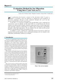
Photo 1 shows the test equipment. Test equipment included a Bench-top Type Temperature<br />
and Humidity Chamber in parallel with a Highly Accelerated Stress Test System (HAST Chamber)<br />
and an Ion Migration Evaluation (Electrochemical Migration Evaluation) System. We used four<br />
sets of temperature and humidity conditions: 60℃ at 85%rh, 85℃ at 85%rh, 110℃ at 85%rh,<br />
and 120℃ at 85%rh. The applied test voltage and the measured test voltage were both 50V DC.<br />
During the tests, we continuously monitored leak current. We used a leak detection cycle that<br />
stopped the application of voltage upon detecting leak current above a pre-set resistance, and<br />
also a leak behavior mode (which triggers a behavior check cycle after confirming leak behavior)<br />
that stopped the application of voltage after being entered above a pre-set number of times. The<br />
standard leak current setting is 1μA (resistance: 5 x 10⁷Ω), and failure time was determined as<br />
either leak current reset, or entering the behavior check cycle in five successive checks done at<br />
one-minute intervals, whichever came first.<br />
Highly Accelerated Stress Test<br />
System (HAST Chamber)<br />
Bench-top Type Temperature and Humidity<br />
Chamber and Ion Migration Evaluation<br />
(Electrochemical Migration Evaluation) System<br />
Photo 1 Test equipment<br />
- 3 -<br />
Espec Technology Report No.24
Evaluating the CAF (conductive anodic filament) resistance of multi-layered PWBs<br />
3<br />
Test specimens<br />
Fig.3 shows a photo and a diagram of the surface pattern of the PWB used in the tests. The<br />
PWB type was an eight-layered FR-4, and we used types A, B (halogen-free), C, and D model<br />
PWBs. Ten throughhole pairs were used on each PWB, with the following relationship of distance<br />
between throughhole walls to size of throughhole diameter (refer to Fig.4): 0.3/0.2, 0.4/0.2,<br />
0.5/0.2, 0.3/0.6, and 0.3/1.0 (units: mm, same below). The throughhole pairs were linked using<br />
a copper pattern, and during the tests each of the ten pairs received voltage application<br />
simultaneously. The specimens were constructed so that after the tests the copper patterns could<br />
be cut apart to permit each throughhole pair to have its resistance measured individually. Using<br />
this method, the resistance of each throughhole pair was measured, and the sites of insulation<br />
degradation were specified.<br />
Fig.3 Photo and diagram of surface pattern<br />
- 4 -<br />
Fig.4 Diagram of PWB with<br />
throughholes cross-sectioned<br />
vertically<br />
Espec Technology Report No.24
Evaluating the CAF (conductive anodic filament) resistance of multi-layered PWBs<br />
Table 2 lists the test conditions and specimens.<br />
Conditions<br />
Specimens<br />
4<br />
Test results<br />
Temp. /Humid.<br />
Table 2 Test conditions and specimens<br />
60℃, 85%rh; 85℃, 85%rh; 110℃, 85%rh;<br />
120℃, 85%rh<br />
Applied voltage Bias voltage: 50 V, Test voltage: 50 V<br />
Material type FR-4(8-layer)<br />
Models PWB A, PWB B (Halogen-free), PWB C, PWB D<br />
PTH wall-to-wall spaces/<br />
Drilled hole sizes<br />
4-1 Behavior of insulation resistance<br />
0.3/0.2, 0.4/0.2, 0.5/0.2, 0.3/0.6, 0.3/1.0<br />
Fig.5 shows the correspondence between time and the behavior of insulation resistance of PWB<br />
C tested at 110℃ and 85%rh. The relationship of distance between throughhole walls to size of<br />
throughhole diameter used was 0.3/0.2. To confirm the behavior of insulation resistance leak<br />
current, standard settings were 50μA (resistance: 1 x 10 6 Ω), continuously testing leading to<br />
failure, with the test ending at approximately 45 hours. Fig.5 indicates that insulation resistance<br />
temporarily drops at the time of CAF formation, with resistance then recovering and the pattern<br />
being repeated.<br />
Fig.5 Behavior of insulation resistance<br />
(50V DC at 110℃ and 85%rh, PWB C, 0.3/0.2)<br />
- 5 -<br />
Espec Technology Report No.24
Evaluating the CAF (conductive anodic filament) resistance of multi-layered PWBs<br />
4-2 Test results for temperature acceleration<br />
Fig.6 shows a Weibull plot for temperature acceleration of specimens at 60℃ and 85%rh, 85℃<br />
and 85%rh, 110℃ and 85%rh, and 120℃ and 85%rh tested at 50V DC for 2400 hours. The<br />
PWB was model C with a relationship of 0.3/0.2 for distance between throughhole walls to size of<br />
throughhole diameter. The “m” in the graph is the shape parameter.<br />
The Weibull plot trends show a difference only for the conditions of 120℃ and 85%rh. The<br />
failure mode in the test at 120℃ and 85%rh differed from the failure modes at the other<br />
temperature and humidity conditions. The conditions of 120℃ and 85%rh in this test may have<br />
been too harsh for the specimens used.<br />
Fig.6 Weibull plot of temperature acceleration<br />
(50V DC for 3000 hours, PWB C, 0.3/0.2)<br />
- 6 -<br />
Espec Technology Report No.24
Evaluating the CAF (conductive anodic filament) resistance of multi-layered PWBs<br />
4-3 Test results for different PWBs<br />
Fig.7 shows a Weibull plot for each type of PWB tested for 500 hours at 110℃ and 85%rh. The<br />
relationship used for the distance between throughhole walls to throughhole diameter was<br />
0.3/0.2.<br />
The test results indicated that PWB C had a shorter time to failure than PWBs A and B.<br />
Only three of the nine specimens of PWB B (halogen-free) failed within the 500 hours of test<br />
time, yielding the longest time leading to failure of any specimen.<br />
Fig.8 shows the humidity absorption characteristics of these PWBs at 110℃ and<br />
85%rh. No correlation was seen between humidity absorption rate and failure time, indicating<br />
that it may be difficult to determine CAF resistance solely on the basis of humidity absorption<br />
characteristics. Factors considered to affect CAF resistance include the flux residue in the inner<br />
layers, the damage to throughhole walls from drilling, and the interface bond between the epoxy<br />
and glass fibers.<br />
Fig.7 Weibull plots for the different PWBs<br />
(50V DC for 500 hours at 110℃,<br />
85%rh, 0.3/0.2)<br />
- 7 -<br />
Fig.8 Humidity absorption<br />
characteristics<br />
(110℃, 85%rh)<br />
Espec Technology Report No.24
Evaluating the CAF (conductive anodic filament) resistance of multi-layered PWBs<br />
4-4 Test results for different distances between throughhole walls and diameter sizes<br />
Fig.9 and 10 show Weibull plots for each specimen based on differing distances between<br />
throughhole walls. The specimens were tested for 3000 hours at 85℃ and 85%rh. PWB C was<br />
used.<br />
With the range of distances between throughhole walls of 0.3 to 0.5 mm, the smaller the<br />
distance between the throughhole walls, the shorter the time leading to failure.<br />
No clear difference was seen among the different throughhole diameters, from 0.2 to 1.0 mm.<br />
The data was not consistent, and so we plan to experiment further.<br />
Fig.9 Weibull plot for each distance<br />
between throughhole walls<br />
(50V DC for 3000 hours at 85℃,<br />
85%rh, PWB C)<br />
- 8 -<br />
Fig.10 Weibull plot for each throughhole<br />
diameter<br />
(50V DC for 3000 hours at 85℃,<br />
85%rh, PWB C )<br />
Espec Technology Report No.24
Evaluating the CAF (conductive anodic filament) resistance of multi-layered PWBs<br />
5<br />
Results of observation<br />
5-1 Results of observation (1)<br />
Fig.11 shows the changes in insulation resistance during the test at 110℃ and 85%rh for PWB<br />
C, Sample 1. The relationship of distance between throughhole walls to size of throughhole<br />
diameter was 0.4/0.2. Approximately 90 hours after test start-up, insulation resistance fell below<br />
5 x 10 5 Ω (marked with a red x in the diagram), and the test was completed. Following the test,<br />
we observed cross sections of the sites of insulation degradation on the PWB.<br />
Fig.11 Changes in insulation resistance (Sample 1)<br />
(50V DC at 110℃ and 85%rh, PWB C, 0.4/0.2)<br />
- 9 -<br />
Espec Technology Report No.24
Evaluating the CAF (conductive anodic filament) resistance of multi-layered PWBs<br />
Photos 2 and 3 are microscope photographs of pre- and post-test specimens. The unevenness<br />
of the throughholes in the pre-test photo is thought to be caused by damage from drilling where<br />
traces of Cu plating have become embedded. In microscopic observation following the test,<br />
substances thought to be CAF were observed along the glass fibers in the epoxy. To obtain a<br />
more detailed analysis, we performed a Cu mapping analysis using a metallurgical microscope<br />
and EPMA (Electron Probe Micro-Analyzer).<br />
Photo 2 Pre-test specimen microscope<br />
image<br />
- 10 -<br />
Photo 3 Post-test specimen microscope<br />
image<br />
(Sample 1)<br />
Photos 4 and 5 are images obtained from the metallurgical microscope and Cu mapping. From<br />
the metallurgical microscope image, this substance is believed to be metallic. From the Cu<br />
mapping image, the main component of the substance is found to be Cu.<br />
Photo 4 Metallurgical microscope image<br />
(Sample 1)<br />
Photo 5 EPMA Cu mapping image<br />
(Sample 1)<br />
Espec Technology Report No.24
Evaluating the CAF (conductive anodic filament) resistance of multi-layered PWBs<br />
5-2 Results of observation (2)<br />
Next, we shall consider changes in insulation resistance during the test, and post-test<br />
observation of insulation degradation sites for Samples 2, 3, and 4 of PWB C at the same test<br />
conditions of 110℃ and 85%rh.<br />
Fig.12, 13, and 14 show changes in insulation resistance for Samples 2, 3, and 4. The green X<br />
in the diagrams indicates the formation of leak touch, with a resistance below 5 x 10 7 Ω. A red X<br />
indicates a resistance of 5×10 5 Ω or below. (However, since the leak current standard setting for<br />
Fig.14 was 50μA, resistance indicated is below 1 x 10 6 Ω.)<br />
The repeated fall and recovery of resistance seen in Fig.13 is conjectured to be repeated<br />
breaking and connecting of a fine section of CAF.<br />
Fig.12 Changes in insulation resistance<br />
(Sample 2)<br />
(50V DC at 110℃ and 85%rh,<br />
PWB C, 0.5/0.2)<br />
Leak current setting, 1μA<br />
(resistance, 5 x 10 7 Ω)<br />
Fig.14 Changes in insulation resistance<br />
(Sample 4)<br />
(50V DC at 110℃ and 85%rh,<br />
PWB C, 0.3/0.2)<br />
Leak current setting, 50μA<br />
(resistance, 1 x 10 6 Ω)<br />
- 11 -<br />
Fig.13 Changes in insulation resistance<br />
(Sample 3)<br />
(50V DC at 110℃ and 85%rh,<br />
PWB C, 0.4/0.2)<br />
Leak current setting, 1μA<br />
(resistance, 5 x 10 7 Ω)<br />
Espec Technology Report No.24
Evaluating the CAF (conductive anodic filament) resistance of multi-layered PWBs<br />
Photos 6 though 9 are post-test microscope images of sites of insulation degradation. For<br />
Samples 1 and 2, the test was concluded when resistance fell below 5 x 10 5 Ω. For Sample 3, the<br />
test was concluded when resistance fell to 7.21 x 10 8 Ω. For Sample 4, the test was concluded<br />
when resistance fell to 5.11 x 10 9 Ω.<br />
Photos 6 through 9 indicate that in the specimens with insulation degradation set at below 5 x<br />
10 5 Ω the CAF diameter is thicker than that in the 7.21 x 10 8 Ω and 5.11 x 10 9 Ω. This experiment<br />
indicates that the density may have increased after the CAF connected the anode and cathode,<br />
leading to insulation degradation.<br />
Photo 6 Site of insulation degradation<br />
(below 5 x 10 5 Ω)<br />
(Sample 1)<br />
Photo 8 Site of insulation degradation<br />
(7.21 x 10 8 Ω)<br />
(Sample 3)<br />
- 12 -<br />
Photo 7 Site of insulation degradation<br />
(below 5 x 10 5 Ω)<br />
(Sample 2)<br />
Photo 9 Site of insulation degradation<br />
(5.11 x 10 9 Ω)<br />
(Sample 4)<br />
Espec Technology Report No.24
Evaluating the CAF (conductive anodic filament) resistance of multi-layered PWBs<br />
5-3 Results of observation (3)<br />
Fig.15 shows changes in insulation resistance during the test at 110℃ and 85%rh for PWB D,<br />
Sample 5. The relationship of distance between throughhole walls to size of throughhole diameter<br />
was 0.3/0.2. Following the test, we observed cross sections of sites of probable insulation<br />
degradation on this PWB. Photos 10 and 11 are microscope images of the pre- and post-test<br />
specimen.<br />
Observation indicated that the insulation degradation on this specimen was not caused by CAF<br />
along glass fibers, but rather by ion migration forming between the core material* and the<br />
prepreg sheets**.<br />
Fig.15 Changes in insulation resistance (Sample 5)<br />
(50V DC at 110℃ and 85%rh, PWB D, 0.3/0.2)<br />
Photo 10 Pre-test microscope image<br />
*Core material: inner layer laminate of multi-layer PWB<br />
**Prepreg sheets: Adhesive sheet used to bond core material layers<br />
- 13 -<br />
Photo 11 Post-test microscope image<br />
(Sample 5)<br />
Espec Technology Report No.24
Evaluating the CAF (conductive anodic filament) resistance of multi-layered PWBs<br />
5-4 Results of observation (4)<br />
Next, we shall consider PWB C Samples 6 and 7 in tests at 110℃ and 85%rh with regard to<br />
examples of CAF observed even in specimens analyzed as non-defective when the test was<br />
concluded prior to insulation degradation. For Sample 6, Fig.16 shows changes in insulation<br />
resistance, Photo 12 is a post-test microscope image, and Photo 13 is a post-test metallurgical<br />
microscope image. For Sample 7, Fig.17 shows changes in insulation resistance, Photo 14 is a<br />
post-test microscope image, and Photo 15 is a post-test metallurgical microscope image.<br />
From Fig.16 and 17 and Photos 12 through 15 we can see that neither Sample 6 nor Sample 7<br />
have any major changes in insulation resistance. However, post-test observation revealed CAF<br />
along the glass fibers. Observation of Sample 7 revealed CAF growing from both the anode and<br />
the cathode, but since three-dimensional observation and observation during the test are<br />
problematic, this did not lead to clarification of the process of CAF growth.<br />
Fig.16 Changes in insulation resistance (Sample 6)<br />
(50V DC at 110℃ and 85%rh, PWB C, 0.3/0.2)<br />
Photo 12 Post-test microscope image<br />
(Sample 6)<br />
- 14 -<br />
Photo 13 Post-test metallurgical<br />
microscope image<br />
(Sample 6)<br />
Espec Technology Report No.24
Evaluating the CAF (conductive anodic filament) resistance of multi-layered PWBs<br />
Fig.17 Changes in insulation resistance (Sample 7)<br />
(50V DC at 110℃ and 85%rh, PWB C, 0.3/0.2)<br />
Photo 14 Post-test microscope image<br />
(Sample 7)<br />
- 15 -<br />
Photo 15 Post-test metallurgical<br />
microscope image<br />
(Sample 7)<br />
Espec Technology Report No.24
Evaluating the CAF (conductive anodic filament) resistance of multi-layered PWBs<br />
5-5 Results of observation (5)<br />
Up to this point, we have considered observation of PWBs with the throughholes<br />
cross-sectioned vertically. Next we shall consider observation of PWBs with the throughholes<br />
cross-sectioned horizontally. Fig.18 shows changes in insulation resistance during the test at<br />
120℃ and 85%rh for PWB D, Sample 8. The relationship of distance between throughhole walls<br />
to size of throughhole diameter was 0.3/0.2. Photo 16 is a pre-test microscope image, while<br />
post-test images of sites of insulation degradation are presented in Photo 17, a microscope<br />
image, and Photo 18, a metallurgical microscope image.<br />
The metallurgical microscope image shows CAF growing from the anode toward the cathode,<br />
and it was confirmed to be extending obliquely toward the back. This is presumed to be caused by<br />
the existence of CAF along the glass fibers.<br />
Fig.18 Changes in insulation resistance<br />
(Sample 8)<br />
(50V DC at 120℃ and 85%rh,<br />
PWB D, 0.3/0.2)<br />
Photo 17 Post-test microscope image<br />
(Sample 8)<br />
- 16 -<br />
Photo 16 Pre-test microscope<br />
image<br />
Photo 18 Post-test metallurgical<br />
microscope image<br />
(Sample 8)<br />
Espec Technology Report No.24
Evaluating the CAF (conductive anodic filament) resistance of multi-layered PWBs<br />
6<br />
We carried out High Temperature and Humidity Tests and Highly-Accelerated Stress Tests<br />
(HAST) to evaluate the CAF resistance of multi-layered PWBs. These experiments produced the<br />
following results.<br />
- At the time of CAF occurrence, insulation resistance exhibits a cyclical behavior of repeatedly<br />
falling temporarily and then recovering.<br />
- PWB C exhibited a shorter time leading to failure than either PWB A or B, but since PWB C did<br />
not exhibit a noticeably high level of humidity absorption in the Humidity Absorption test,<br />
determining CAF resistance characteristics solely on the basis of humidity absorption<br />
characteristics seems to be problematic.<br />
- The tests at 120℃ and 85%rh may have been too harsh for the PWB C specimen used in these<br />
tests, so that the failure mode may have been different from the failure mode at the other<br />
conditions of temperature and humidity.<br />
- CAF along the glass fibers and a substance believed to be ion migration occurring between the<br />
core material and the prepreg sheets were observed at presumed sites of insulation<br />
degradation. In addition, CAF occurrence was observed in specimens that did not exhibit<br />
insulation degradation.<br />
7<br />
Conclusion<br />
Challenges for further research<br />
In this research, we observed CAF growing from the anode as well as from the cathode, and we<br />
plan to carry out further research regarding the growth process and mechanism. In addition,<br />
investigation is required on what effect the manufacturing conditions and pre-conditioning of<br />
multi-layered PWBs have on the formation and growth of CAF.<br />
It must be stressed that the evaluations produced by this research are relative, and their<br />
correlation to actual failure in the field are a challenge for further research. We plan to carry out<br />
further reliability testing with other temperature and humidity conditions to investigate<br />
accelerated temperature and humidity characteristics.<br />
[Bibliography]<br />
1) L. J. Turbini, Ph.D.: “Conductive Anodic Filament (CAF) Formation: An Historic Perspective”,<br />
ECWC10 Conference, 2005.<br />
2) F. Ishigami, H Sakai, and Y. Nakamura, Hitachi Chemical Technical Report, No.39, pp.25-28,<br />
2002.<br />
3) M. Miyatake, H. Murai, T. Fukuda, and S. Shimaoka, Hitachi Chemical Technical Report, No.45,<br />
pp.31-35, 2005.<br />
4) Y. Nakamura, T. Asano, and N. Ito, Matsushita Electric Technical Report, No.75, pp.14-18,<br />
2001.<br />
5) K. Komori, T. Watanabe, and Y. Matsushita, “Low-Dielectric-Constant Multi-layer PCB Material<br />
‘MEGRON5,’” Matsushita Electric Technical Report, Vol.52, No.1, pp.23-27, 2004.<br />
- 17 -<br />
Espec Technology Report No.24
New JTM standards for temperature test chambers - Methods of testing and indicating performance<br />
Understanding the Technology<br />
New JTM standards for temperature test chambers<br />
- Methods of testing and indicating performance<br />
Toshimi Ishida Environmental Test Business Headquarters, Business Control Department<br />
J<br />
apan Testing Machinery Association (JTM) has established standards for<br />
environmental test equipment.<br />
JTM has issued a new standard for environmental test chambers called JTM K 07,<br />
"Temperature chambers-Test and indication method for performance". This<br />
standard conforms to standards established by IEC (International<br />
Electrotechnical Commission) and JIS (the Japanese Standards Association), and<br />
has major changes from previous methods of testing and indicating performance<br />
for environmental test equipment. As a result, we would like to present the<br />
background leading to the establishment of this standard as well as its principal<br />
contents. In addition, we would like to discuss the coming trends in methods of<br />
testing and indicating performance for temperature and humidity test chambers.<br />
1<br />
Trends in standards for environmental test equipment<br />
Efforts to standardize environmental test equipment have been under way continuously since<br />
the "Engineering industry standardization project" of 1975. In 1976, MITI (the Ministry of<br />
International Trade and Industry) organized special committees to promote standardization,<br />
including the Japan Machinery Federation (JMF), Japan Testing Machinery Association (JTM), and<br />
related organizations, and investigations began on means of standardization. Following that,<br />
investigative research from those committees began accumulating, and JTM established<br />
standards related to performance and safety. Below is a list of the establishment and revision of<br />
some of the major performance standards.<br />
1985: JTM K 01, Temperature and humidity chambers - Test and indication method for<br />
performance (Established)<br />
1988: JTM K 03, Environmental temperature and humidity rooms - Test and indication<br />
method for performance (Established)<br />
1991: JTM K 05, High temperature chambers - Test and indication method for performance<br />
(Established)<br />
1998: JTM K 01 (Revised)<br />
2000: JTM K 05 (Revised)<br />
2001: JTM K 03 (Revised)<br />
- 18 -<br />
Espec Technology Report No.24
New JTM standards for temperature test chambers - Methods of testing and indicating performance<br />
The driving force for promoting environmental testing software has included the United States<br />
military standards (MIL) and the IEC and JIS standardization of electrical, automotive, and<br />
maritime standards. JTM has been at the forefront for promoting the standardization of<br />
hardware. These industrial standards have been established for the purpose of contributing to the<br />
improvement and maintenance of product quality and to international standardization.<br />
The IEC standards and JIS standards for environmental test equipment have been established<br />
as follows.<br />
2001: IEC 60068-3-5, Environmental testing - Part 3-5: Supporting documentation and<br />
guidance - Confirmation of the performance of temperature chambers<br />
2006: JIS C 60068-3-5, Environmental testing - Part 3-5: Supporting documentation and<br />
guidance - Confirmation of the performance of temperature chambers<br />
The contents of this JIS standard matches the contents of the above IEC standard. The IEC and<br />
JIS standards for temperature test chambers are utilized for all equipment used in environmental<br />
testing and are provided for the general use of the user to confirm the performance of test<br />
chambers. Since these standards constitute guidance, there is a danger that when put into<br />
practice they may be subject to a number of interpretations. Because of that, JTM has taken a<br />
proper understanding of the contents of these standards, and including portions that are unclear<br />
or not stipulated in the standards as well as contents that made up the previous JTM standards<br />
has developed new JTM standards.<br />
The new JTM standards target the “temperature test chambers” and have changed the<br />
contents of JTM K 01 (Temperature and humidity chambers - Test and indication method for<br />
performance), JTM K 03 (Environmental temperature and humidity rooms - Test and indication<br />
method for performance), and JTM K 05 (High temperature chambers - Test and indication<br />
method for performance) to create the new JTM standards. However, the new standards will be<br />
phased in over the course of 5 years following their publication.<br />
In addition, JTM is planning to publish new standards targeting “temperature and humidity test<br />
chambers” as well.<br />
- 19 -<br />
Espec Technology Report No.24
New JTM standards for temperature test chambers - Methods of testing and indicating performance<br />
2<br />
Table 1 presents an overview of the major revisions to the standards.<br />
Method of indicating<br />
performance<br />
Method of confirming performance<br />
New test and indication methods for performance<br />
Distance of<br />
working<br />
space<br />
Range of temp.<br />
fluctuation<br />
Temp.<br />
uniformity<br />
Heating/cooling<br />
time<br />
Table 1 Principal changes in the new JTM standards<br />
Current standards New standards Comments<br />
Range of temp. fluctuation Temp. fluctuation Method of confirming<br />
performance also<br />
changed<br />
Temp. uniformity Temp. gradient, Temp.<br />
variation in space<br />
- 20 -<br />
Method of confirming<br />
performance also<br />
changed<br />
Heating/cooling time Temp. rate of change Method of confirming<br />
performance also<br />
changed<br />
Space excluding 1/6 of<br />
distance from inner walls<br />
Measurement point: single<br />
point at center of chamber<br />
Calculation method: take the<br />
difference between average<br />
high and average low temps,<br />
divide by two, and express as<br />
± value<br />
Concept: Difference between<br />
center of chamber and 8 corner<br />
points<br />
Definition: Time required to<br />
reach max/min temp. from<br />
ambient temp.<br />
Expression: n1℃ to n2℃,<br />
x minutes<br />
Let’s consider the major points of the new standards.<br />
Space excluding 1/10 of<br />
distance from inner walls<br />
Measurement points: 9 points<br />
(chamber center and 8<br />
corners)<br />
Calculation method: take the<br />
highest value of the standard<br />
deviation among all of the<br />
measurement points, double it,<br />
and express as ± value.<br />
Concept: Difference between<br />
center of chamber and 8 corner<br />
points, and difference among<br />
corners<br />
Definition: Rate of temp.<br />
change during one minute for<br />
specified times<br />
Expression:K/minute or ℃<br />
/minute<br />
Minimum values<br />
specified for different<br />
test chamber volumes<br />
Time to reach temp.<br />
extreme conforms to<br />
prior<br />
heating/cooling<br />
time<br />
Espec Technology Report No.24
New JTM standards for temperature test chambers - Methods of testing and indicating performance<br />
2-1 Working space<br />
The working space is a test chamber area that can maintain specified temperature conditions<br />
within an allowable range. The test chamber generally takes the shape of a rectangular box, and<br />
the working space is composed of the area surrounded by the shaded surface shown in Fig.1. The<br />
distance from each of the wall surfaces surrounding the working space to the next corresponding<br />
chamber surface shall be termed as L1, L2, and L3, respectively. Current standards define the<br />
working space as the space between the surrounding walls excluding the area adjacent to the<br />
walls composed of a distance divided by 6 from the total surface distance, expressed as L1/6, L2/6, and L3/6. The new standards define the working space as the space between the<br />
surrounding walls excluding the area adjacent to the walls composed of a distance divided by 10<br />
from the total surface distance, expressed as L1/10, L2/10, and L3/10. However, since it is<br />
necessary to consider the effect of thermal emissions in the space between the inner walls of the<br />
test chamber and the test specimens, the distance from the inner walls must be specified as a<br />
minimum value according to the volume of each test chamber.<br />
Fig.1 Working space<br />
- 21 -<br />
Espec Technology Report No.24
New JTM standards for temperature test chambers - Methods of testing and indicating performance<br />
2-2 Range of temperature fluctuation<br />
The range of temperature fluctuation in the current standards is defined as the difference<br />
between the average high temperature and the average low temperature at the center of the test<br />
chamber. The new standards refer to temperature fluctuation, which is defined as the<br />
difference between the maximum and minimum temperatures at discretionary points in the<br />
working space measured at specified time intervals after the temperature has stabilized. The new<br />
standards have set the discretionary points as being at the center and at the corners of the<br />
working space. As can be seen in Fig.2, to find the range of fluctuation according to current<br />
standards, average temperatures are first calculated for a measured point in the center of the<br />
chamber. Then, the average temperatures are separated into high and low temperatures and the<br />
average high and low temperatures are calculated, and the fluctuation is defined as the difference<br />
between these high and low averages. This difference is divided by two, and then that result is<br />
displayed as a ± value.<br />
Fig.2 Temperature fluctuation in current standards<br />
The calculation method used by the current standards is as follows.<br />
Average temp. =<br />
Average high temp. =<br />
Average low temp. =<br />
Range of temperature fluctuation = ±(average high temp. - average low temp.)/2<br />
- 22 -<br />
Espec Technology Report No.24
New JTM standards for temperature test chambers - Methods of testing and indicating performance<br />
No specific measurement procedures are presented in JIS C 60068-3-5 (IEC 60068-3-5).<br />
Actual measurements are performed at user-selected sampling intervals, and so one cannot say<br />
that the data has necessarily captured the peak temperatures.<br />
The new standards call for statistical estimation of temperature fluctuation. After the<br />
temperature has stabilized, the temperature is measured at regular intervals at the specific<br />
measurement points, a minimum of 10 times for 30 minutes, and is represented as X1,X2, …Xi… X n (n ≧10). XAve represents the average value of X, and in X i, the i represents a number from 1<br />
to n. Using these, the σ n-1 specimen standard deviation is defined as follows.<br />
Temperature fluctuation is found by taking ±2σn-1 for each of the 9 measurement points inside<br />
the working space and notating the greatest of these values as the temperature fluctuation. Units<br />
are represented in K (Kelvin, absolute temperature) or ℃ (Celsius).<br />
Fig.3 Temperature fluctuation in new standards<br />
- 23 -<br />
Espec Technology Report No.24
New JTM standards for temperature test chambers - Methods of testing and indicating performance<br />
2-3 Temperature uniformity<br />
In the current standards, temperature uniformity is defined as the temperature differential<br />
between the temperature at the center of the chamber and discretionary points in the working<br />
space. For the high temperature chamber or the temperature and humidity chamber,<br />
measurements are taken at a minimum of five points, which include the center of the chamber<br />
and at selected symmetrical points around the center, four of which are as far from the center as<br />
possible. For the temperature and humidity chamber, measurements are taken at nine points,<br />
which include at the center of the chamber and at each of the eight apices. First the average<br />
temperatures are calculated for each point, and then the average temperature at the center point<br />
is divided by the high and low temperatures. Next, the average temperatures are found for the<br />
high-temperature and low-temperature points. The temperature uniformity is the difference<br />
between the high and low average temperatures. This value is displayed as a ± value divided by<br />
2.<br />
The new standards, however, do not use the expression temperature uniformity, opting instead<br />
for the two terms temperature variation in space and temperature gradient.<br />
Temperature variation in space refers to the difference in average temperature between the<br />
center of the working space and separate discretionary points at some point in time after the<br />
temperature has stabilized. Measurements are taken at nine points: at the center of the working<br />
space and at the eight apices.<br />
Temperature variation in space is defined as the maximum average difference between the<br />
average temperature at the center of the working space and the average temperatures at each of<br />
the other measurement points. This difference is expressed as an absolute value.<br />
Average temperature at the center of the working space: XCenterAve<br />
Average temperature at each of the working space apices: XCornerAve(j); j = 1 to 8<br />
Temperature variation in space = |Max(XCornerAve(j) - XCenterAve)|<br />
The temperature gradient is the greatest average difference between the average<br />
temperatures at two separate points within the working space at discretionary points in time after<br />
the temperature has stabilized. The nine measurement points are specified as at the center of the<br />
working space and at the eight apices. The temperature gradient is defined as the maximum<br />
difference in average temperature among the measurement points.<br />
Maximum average temperature at each measurement point: XAveMax<br />
Minimum average temperature at each measurement point: XAveMin<br />
Temperature gradient = XAveMax - XAveMin<br />
To sum up, temperature variation in space indicates how great a difference exists between the<br />
center of the working space and the rest of the working space. Temperature gradient indicates<br />
how great a difference exists among each of the various points in the working space. The two<br />
terms together express the concept of temperature uniformity.<br />
- 24 -<br />
Espec Technology Report No.24
New JTM standards for temperature test chambers - Methods of testing and indicating performance<br />
2-4 Heating and cooling time<br />
In the current standards, heating and cooling time refers to the time required to reach the<br />
maximum or minimum temperature of the temperature control range from the ambient<br />
temperature under standard conditions at the center of the chamber. In the new standards, this<br />
term has been replaced with time to reach temperature extremes. The new standards have<br />
also added the term temperature rate of change. The temperature rate of change indicates<br />
the temperature for one minute, and refers to measuring the rate of temperature change<br />
between two specified points in time at the center of the working space. Fig.4 shows rate of<br />
change for an interval ten percent prior to both the maximum and minimum temperatures.<br />
Fig.4 Temperature rate of change for heating and cooling a test chamber<br />
The temperature rate of change is found using the following formula.<br />
Temperature heating rate = △ t/T1 Temperature cooling rate = △ t/T2 The closer the temperature comes to the maximum or minimum temperature, the slower the<br />
rate of change, and so the temperature rate of change excludes that portion just prior to reaching<br />
maximum or minimum temperature. Because of this, it is not possible to know the actual time at<br />
which the maximum or minimum temperature is reached. Therefore, the heating and cooling<br />
time of the previous standard has changed only in its expression as time to reach temperature<br />
extremes, but the content adheres to the current concept with no change. The time to reach<br />
temperature extremes refers to the time to reach or pass through the temperature extreme from<br />
the ambient temperature under standard conditions at the center of the working space.<br />
- 25 -<br />
Espec Technology Report No.24
New JTM standards for temperature test chambers - Methods of testing and indicating performance<br />
3<br />
Current standards and the activation of new standards<br />
The current standards will expire five years after the publication of the new standards. The new<br />
standards are for the temperature test chamber. At the current stage JIS has not yet<br />
published new standards for the temperature and humidity test chamber, and so the new<br />
standards for the temperature test chamber will precede those for the temperature and humidity<br />
test chamber. As a result, current standards will continue to apply to the temperature and<br />
humidity test chamber, and only those contents concerning the temperature test chamber will<br />
proceed to application of the new standards.<br />
Table 2 Test chambers and standards subject to transition to new standards<br />
Current<br />
standard<br />
number<br />
JTM K01<br />
JTM K03<br />
JTM K05<br />
Name of test chamber<br />
subject to current<br />
standard<br />
Temperature chamber Transition to K07 as<br />
temperature test<br />
chamber<br />
Temperature and Current standard K01<br />
humidity chamber stays in effect<br />
Temperature room Transition to K07 as<br />
temperature test<br />
chamber<br />
Temperature and Current standard K01<br />
humidity room<br />
stays in effect<br />
High temperature<br />
chamber<br />
Details of transition Comments<br />
Full transition to K07 as<br />
temperature test<br />
chamber<br />
- 26 -<br />
Measure expires 5<br />
years after transition<br />
Enactment of newer<br />
standard already<br />
planned<br />
Measure expires 5<br />
years after transition<br />
Enactment of newer<br />
standard already<br />
planned<br />
Measure expires 5<br />
years after transition<br />
Espec Technology Report No.24
New JTM standards for temperature test chambers - Methods of testing and indicating performance<br />
4<br />
Coming standards<br />
The current standards have been established over a long period of time utilizing both domestic<br />
and foreign investigations as JTM has worked to standardize environmental testing equipment.<br />
The current standards are used not only in Japan but also around the world.<br />
IEC 60068-3-5, enacted in 2001, has finally become a global standard. Five years have elapsed<br />
since its enactment as an international standard, and yet this standard is still not widely accepted<br />
throughout the world. In Europe there are wide variations in how this standard is applied. In<br />
America and Asia, even the contents are not well known.<br />
JIS C 60068-3-5 was enacted in 2006, and so there has been a lot of discussion in Japan as to<br />
whether new JTM standards are necessary. The new JTM standards will not bring about changes<br />
in the hardware for environmental testing equipment, but rather will bring about changes in<br />
testing methods and in ways of indicating or expressing performance. Therefore, although the<br />
equipment may be the same, there is some concern that these changes have produced the<br />
misunderstanding that a loss of performance has occurred.<br />
However, if we should disregard this international standard and remain at the current stage of<br />
domestic industrial standards, the situation would not be conducive to preparing for the coming<br />
global development. Japan Testing Machinery Association has borne the mission of supporting<br />
the development of the Japanese testing technology and the environmental equipment testing<br />
technology that have laid the foundation for the high quality of Japanese products, and JTM will<br />
bear the mission for taking a leading role globally in the future as well. Because of this, the new<br />
JTM standard is coordinated with the contents of the IEC 60068-3-5 standard, supplementing<br />
obscure points and producing a more well-developed standard.<br />
Regarding temperature and humidity test chambers, the IEC 60068-3-6 standard was enacted<br />
in 2001. For this international standard as well, JTM plans to create a new JTM standard that<br />
supplements the obscure points and further develops the standard.<br />
- 27 -<br />
Espec Technology Report No.24
New JTM standards for temperature test chambers - Methods of testing and indicating performance<br />
5<br />
Conclusion<br />
The IEC and JIS standards for temperature test chambers are utilized for all equipment used in<br />
environmental testing and are provided for the general use of the user to confirm the<br />
performance of test chambers. However, the contents are guidance, and there is a danger that<br />
they can be subject to all kinds of interpretations when applied. To eliminate the variations caused<br />
by the interpretations among different users, we highly recommend that the new standards<br />
published by JTM be confirmed.<br />
[Bibliography]<br />
1) The Japan Machinery Federation : 1981, Japan Testing Machinery Association: Investigative<br />
report for the standardization of temperature and humidity equipment<br />
2) The Japan Machinery Federation : 1986, Japan Testing Machinery Association: Investigative<br />
research report for the standardization of temperature and humidity rooms<br />
3) JIS C 60068-3-5: 2006, Environmental testing - Part 3-5: Supporting documentation and<br />
guidance - Confirmation of the performance of temperature chambers<br />
4) IEC 60068-3-5: 2001, Environmental testing - Part 3-5: Supporting documentation and<br />
guidance - Confirmation of the performance of temperature chambers<br />
5) Japan Testing Machinery Association: 1994, Investigative research report for the<br />
standardization of measurement and control technology for environmental equipment<br />
6) Japan Testing Machinery Association: 1995, Investigative research report for the<br />
standardization of measurement and control technology for environmental equipment<br />
7) JTM K 01: 1998, Temperature and humidity chambers - Test and indication method for<br />
performance<br />
8) JTM K 03: 2001, Environmental temperature and humidity rooms - Test and indication method<br />
for performance<br />
9) JTM K 05: 2000, High temperature chambers - Test and indication method for performance<br />
- 28 -<br />
Espec Technology Report No.24
New model: Super Clean Oven SCO-2<br />
Topic<br />
New model: Super Clean Oven SCO-2<br />
Kazuhiro Sakonaka, Manabu Shirahase Flat Panel Display Products Division<br />
1<br />
Introduction<br />
We at Espec are proud to present our new 500℃ clean oven, perfectly suited to flat panel<br />
display manufacturing processes such as field emission displays, low-temperature polysilicon,<br />
and organic electroluminescence. This model maintains a high Class 4 (0.3μm) classification for<br />
air cleanliness at all temperature ranges, including temperature ramp-up and cool-down, as well<br />
as during heat treatment at oxygen concentrations of 10 ppm and below.<br />
This new oven not only offers a space-saving slim design, it reduces the environmental load by<br />
more than half from previous models by virtue of features such as low energy and low nitrogen<br />
gas consumption.<br />
Photo 1 Super Clean Oven<br />
- 29 -<br />
Espec Technology Report No.24
New model: Super Clean Oven SCO-2<br />
2<br />
Product features<br />
2-1 Moving up to Class 4 (0.3μm) classification for air cleanliness<br />
Previous ovens have had difficulty maintaining the level of cleanliness during heat ramp up and<br />
cool down, but the new Espec proprietary oven construction utilizes a special heat-resistant filter<br />
that attains the Class 4 (0.3μm) classification for air cleanliness in accordance with<br />
ISO14644-1/JIS B9920 (previously Class 10 under the canceled FED-STD-209E standard) not<br />
only at stable temperatures but during temperature change as well, reducing the amount of<br />
particulate matter falling onto the glass.<br />
How we moved up to Class 4 (0.3μm) classification for air cleanliness<br />
- Using the special high-heat-resistant filter developed by Espec for this model as well enables<br />
continuous operation up to a maximum 500℃. In addition, this filter makes it possible to<br />
maintain a high level of cleanliness even during temperature ramp up and cool down. Using this<br />
special heat-resistant filter at 500℃ delivers a clean oven in a hot air circulation environment.<br />
- We simplified the air conditioning method, rearranging the water-cooled heat exchanger<br />
placement and eliminating the damper inside the chamber. In this way, we were able to<br />
eliminate the sliding section that could generate dust particles.<br />
- By undertaking a fundamental reappraisal of the sheet metal construction and parts inside the<br />
chamber, we were able to minimize the contact and friction of the sheet metal and parts caused<br />
by thermal stretching.<br />
Fig.1 Level of cleanliness at 500℃ operation<br />
- 30 -<br />
Espec Technology Report No.24
New model: Super Clean Oven SCO-2<br />
Fig.2 Level of cleanliness at 400℃ operation<br />
Fig.3 Level of cleanliness at 300℃ operation<br />
- 31 -<br />
Espec Technology Report No.24
New model: Super Clean Oven SCO-2<br />
2-2 Improved temperature uniformity<br />
Rearranging the water-cooled heat exchanger placement allowed us to eliminate the damper.<br />
This new design simplifies the air conditioning method, making it easier to maintain temperature<br />
uniformity.<br />
How we attained improved temperature uniformity<br />
- When we simplified the air conditioning method by moving the water-cooled heat exchanger<br />
and eliminating the damper from inside the chambers, pressure loss was reduced, making it<br />
possible to increase the quantity of circulation air that is required to maintain performance.<br />
- Eliminating excess space required for air conditioning also achieves a space-saving design while<br />
maintaining sufficient double inner walls and sufficient air insulation space on all sides of the<br />
inner chamber racks.<br />
- In addition, we revised the insulation materials, using new materials with a smaller coefficient<br />
of thermal conductivity.<br />
Fig.4 Temperature uniformity at 500℃ operation<br />
- 32 -<br />
Espec Technology Report No.24
New model: Super Clean Oven SCO-2<br />
Fig.5 Temperature uniformity at 400℃ operation<br />
Fig.6 Temperature uniformity at 300℃ operation<br />
- 33 -<br />
Espec Technology Report No.24
New model: Super Clean Oven SCO-2<br />
2-3 Heat treatment capability in a low-oxygen atmosphere<br />
Heat treatment is possible not only during temperature ramp up and at stable temperatures,<br />
but is now possible during cool down as well, even in low-oxygen atmospheres of 10 ppm oxygen<br />
or less.<br />
Fig.7 Oxygen concentration at 500℃ operation<br />
How we achieved heat treatment in a low-oxygen atmosphere<br />
- The cooling method consists of circulating out the hot air, and so in general cooling is achieved<br />
by means of introducing outside air into the chamber. However, with low oxygen specifications,<br />
a water-cooled heat exchanger* replaces the induction of outside air to achieve a hermetically<br />
sealed construction. The introduction of a minimal amount of nitrogen gas is used to attain an<br />
oxygen concentration of 10 ppm inside the chamber.<br />
- Sensors on every port leading to the inside of the chamber are used to maintain the<br />
hermetically sealed environment with the use of metal seals.<br />
*The water-cooled heat exchanger is not placed inside the chamber, and so safety is maintained<br />
with no danger of the water boiling when the operation is stopped at 500℃.<br />
- 34 -<br />
Espec Technology Report No.24
New model: Super Clean Oven SCO-2<br />
2-4 Energy-efficient and space-saving<br />
By revising air conditioning and cooling methods, materials used inside the chamber, heaters,<br />
circulating fans, and the construction of heat-resistant filters, we have been able to reduce by half<br />
the “equipment footprint,” “power consumption,” and “nitrogen usage (at low oxygen<br />
concentrations only)” when compared to our previous HTC-70A model.<br />
2-4-1 How we reduced the equipment footprint by half<br />
We undertook a fundamental reappraisal of the water-cooled heat exchanger placement with<br />
special regard to the standards for low oxygen concentration specifications. The results of this<br />
reappraisal led to the elimination of the damper that was inside the chamber. By eliminating<br />
excess air conditioning space, we were able to reduce the overall size of the oven from 11 m 2 to<br />
6 m 2 . The elimination of the damper reduced the maintenance area as well. (Compared to the<br />
Espec HTC-70A)<br />
Fig.8 Comparison of equipment footprint<br />
2-4-2 How we reduced power consumption by half<br />
Eliminating the excess air conditioning space reduced the amount of heat required inside the<br />
chamber, making it possible to cut the number of circulating fans in half, from two to one, and<br />
reducing the heater capacity from 54.6 kW to 24 kW. This cut our power consumption in half.<br />
(Compared to the Espec HTC-70A)<br />
2-4-3 How we reduced nitrogen usage by half<br />
The reduced volume of the chamber and the reduced number of circulating fans, from two to<br />
one, cut the nitrogen requirement in half. We were able to lower the replacement nitrogen to<br />
500 L/min. (Compared to the Espec HTC-70A)<br />
- 35 -<br />
Espec Technology Report No.24
New model: Super Clean Oven SCO-2<br />
3<br />
Specifications<br />
Table 1 shows the main specifications of the new oven. Fig.9 shows door operation, and Fig.10<br />
shows a detailed diagram of the oven construction.<br />
Table 1 Main specifications<br />
Model No. SCO-1 (Glass accommodation: max. 400 x 500 mm)<br />
Temperature range +100℃ to +500℃<br />
Temperature<br />
uniformity<br />
SCO-2 (Glass accommodation: max. 650 x 750 mm)<br />
SCO-4 (Glass accommodation: max. 800 x 1300 mm)<br />
±3.0℃ (at 300℃)<br />
±4.0℃ (at 400℃)<br />
±5.0℃ (at 500℃)<br />
Level of cleanliness Class 4, 0.3μm<br />
Nitrogen consumption 500 L/min. (SCO-2)<br />
(equiv. to Class 10 of former FED-STD-209E)<br />
Power consumption 200 V AC, 3φ, 29 kVA (SCO-2)<br />
Please contact us for information about other models and voltages.<br />
Fig.9 Oven door operation<br />
- 36 -<br />
Espec Technology Report No.24
New model: Super Clean Oven SCO-2<br />
4<br />
Conclusion<br />
Fig.10 Oven construction<br />
4-1 Effect of manufacturing conditions of MEA specimens<br />
The Super Clean Oven SCO-2 is not only perfectly suited to flat panel display manufacturing<br />
processes such as field emission displays, low-temperature polysilicon, and organic<br />
electroluminescence, this oven is also well-suited as research equipment for applications such as<br />
improving other manufacturing processes and developing materials.<br />
Contact information<br />
For further information on the Super Clean Oven SCO-2, or to request a catalog, please contact<br />
the Espec Corporation System Sales Engineering Department of Flat Panel Display Products<br />
Division.<br />
- 37 -<br />
Espec Technology Report No.24