

Effective PCB Design: - Freescale
Effective PCB Design: - Freescale
Effective PCB Design: - Freescale

You also want an ePaper? Increase the reach of your titles
YUMPU automatically turns print PDFs into web optimized ePapers that Google loves.
<strong>Effective</strong> <strong>PCB</strong> <strong>Design</strong>:<br />
Techniques to improve performance<br />
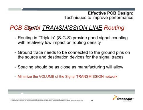
<strong>PCB</strong> Signal TRANSMISSION LINE Routing<br />
• Routing in “Triplets” (S-G-S) provide good signal coupling<br />
with relatively low impact on routing density<br />
• Ground trace needs to be connected to the ground pins on<br />
the source and destination devices for the signal traces<br />
• Spacing should be as close as manufacturing will allow<br />
• Mi Minimize i i the th VOLUME of f the th Signal Si l TRANSMISSION network t k<br />
<strong>Freescale</strong> Semiconductor Confidential and Proprietary Information. <strong>Freescale</strong> and the <strong>Freescale</strong> logo are trademarks<br />
of <strong>Freescale</strong> Semiconductor, Inc. All other product or service names are the property of their respective owners. © <strong>Freescale</strong> Semiconductor, Inc. 2010. 46<br />
TM


