Open PDF
Open PDF
Open PDF
Create successful ePaper yourself
Turn your PDF publications into a flip-book with our unique Google optimized e-Paper software.
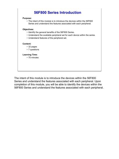
56F800 Series Introduction<br />
Purpose:<br />
• The intent of this module is to introduce the devices within the 56F800<br />
Series and understand the features associated with each peripheral.<br />
Objectives:<br />
• Identify the general benefits of the 56F800 Series.<br />
• Understand the available peripheral set for each device within the series.<br />
• Understand features of the peripheral set.<br />
Content:<br />
• 32 pages<br />
• 7 questions<br />
Learning Time:<br />
• 70 minutes<br />
The intent of this module is to introduce the devices within the 56F800<br />
Series and understand the features associated with each peripheral. Upon<br />
completion of this module, you will be able to identify the devices within the<br />
56F800 Series and understand the features associated with each peripheral.
Why 56F800?<br />
• MCU functionality and DSP performance<br />
resulting from a hybrid architecture<br />
• 30 & 40 MIPS FLASH performance<br />
• Reduction in system costs due to highly<br />
integrated features<br />
• Aggressive prices<br />
• Proven success - hundreds of applications in<br />
production today<br />
• New SW tools strategy supports low-cost<br />
development<br />
• Targets motor control for industrial, appliance,<br />
medical, and home/office environments<br />
• Continual investment into family<br />
The 56F800 series provides MCU functionality and DSP performance with its<br />
56800 Core hybrid architecture. This series integrates 40 MIPs FLASH<br />
performance and a host of other integrated features that reduce the overall<br />
system cost. The peripheral set is targeting motor control applications but<br />
has also been successful as a general purpose controller. Its feature set and<br />
aggressive pricing has met the market needs as proven by the hundreds of<br />
applications in production today. This series is just another example of our<br />
dedication to continual investment in its Hybrid Controller portfolio.
56F800 Features<br />
Program<br />
FLASH<br />
JTAG/OnCE<br />
Voltage<br />
Regulators<br />
Interrupt<br />
Controller<br />
Power<br />
Supervisor<br />
COP<br />
SCI0<br />
SCI1<br />
SPI<br />
MSCAN<br />
GPIOs<br />
Relax. OSC<br />
System Clock<br />
Generator<br />
(OSC & PLL)<br />
Program<br />
Boot<br />
RAM<br />
FLASH<br />
56800<br />
Core<br />
30-40 MIPS<br />
60-80 MHz<br />
2x4 input<br />
2x4 input<br />
ADC<br />
ADC<br />
Module A<br />
Module B<br />
External<br />
Memory<br />
Interface<br />
Data RAM<br />
Data FLASH<br />
6-output<br />
PWM A<br />
6-output<br />
PWM B<br />
Quad Timer<br />
Module A,B,C,D<br />
Quadrature<br />
Decoder 0<br />
Quadrature<br />
Decoder 1<br />
56F801<br />
56F802<br />
56F803<br />
56F805<br />
56F807<br />
32 – 160 pins<br />
Here, you can see the overall features of the 56F80x family of parts. You<br />
can also see the peripherals associated with each specific part. Roll your<br />
mouse pointer over each feature for more information; then, select the<br />
specific processor derivative to view available peripheral blocks for that<br />
processor.
56F801 Features<br />
Program<br />
FLASH<br />
JTAG/OnCE<br />
Voltage<br />
Regulators<br />
Interrupt<br />
Controller<br />
Power<br />
Supervisor<br />
COP<br />
SCI0<br />
SPI<br />
Program<br />
Boot<br />
RAM<br />
FLASH<br />
56800<br />
Core<br />
30-40 MIPS<br />
60-80 MHz<br />
Data RAM<br />
Data FLASH<br />
6-output<br />
PWM A<br />
Quad Timer<br />
Module C,D<br />
56F801<br />
56F802<br />
56F803<br />
56F805<br />
GPIOs<br />
Relax. OSC<br />
System Clock<br />
Generator<br />
(OSC & PLL)<br />
2x4 input<br />
ADC<br />
Module A<br />
56F807<br />
48 pin LQFP<br />
Now, let’s discuss the features of the other 56F800 products. The 56F801 comes in a 48-pin<br />
LQFP configuration and is available in two maximum speeds: 80MHz/40MIPs and<br />
60MHz/30MIPs.<br />
The 56F801 has a peripheral set that, in addition to being optimal for motion and power<br />
control applications, is also very well-suited to address the needs and demands of the<br />
general-purpose market.
56F802 Features<br />
Program<br />
FLASH<br />
JTAG/OnCE<br />
Voltage<br />
Regulators<br />
Interrupt<br />
Controller<br />
Power<br />
Supervisor<br />
COP<br />
SCI0<br />
SPI<br />
GPIOs<br />
Relax. OSC<br />
System Clock<br />
Generator<br />
(OSC & PLL)<br />
Program<br />
Boot<br />
RAM<br />
FLASH<br />
56800<br />
Core<br />
30-40 MIPS<br />
60-80 MHz<br />
1x2 input<br />
1x3 input<br />
ADC<br />
Data RAM<br />
Data FLASH<br />
6-output<br />
PWM A<br />
Quad Timer<br />
Module C,D<br />
56F801<br />
56F802<br />
56F803<br />
56F805<br />
56F807<br />
32 pin LQFP<br />
Now, let’s look at the features of the 56F802 and its peripherals. The 56F802<br />
has the lowest pin count in the 56F80x family. It too is available in two<br />
maximum speeds: 80MHz/40MIPs and 60MHz/30MIPs. It further extends<br />
the 56F800 family down to better support low cost applications.
56F803 Features<br />
Program<br />
FLASH<br />
JTAG/OnCE<br />
Voltage<br />
Regulators<br />
Interrupt<br />
Controller<br />
Power<br />
Supervisor<br />
COP<br />
SCI0<br />
SPI<br />
MSCAN<br />
GPIOs<br />
Program<br />
Boot<br />
RAM<br />
FLASH<br />
56800<br />
Core<br />
40 MIPS<br />
80 MHz<br />
External<br />
Memory<br />
Interface<br />
Data RAM<br />
Data FLASH<br />
6-output<br />
PWM A<br />
Quad Timer<br />
Module A,C,D<br />
Quadrature<br />
Decoder 0<br />
56F801<br />
56F802<br />
56F803<br />
56F805<br />
56F807<br />
System Clock<br />
Generator<br />
(OSC & PLL)<br />
2x4 input<br />
ADC<br />
Module A<br />
100 pin LQFP<br />
Here, we can see the features of the 56F803 and its peripherals. Compared to the 56F801<br />
and 56F802, the 56F803 contains some additional features. These include 32K words of<br />
Program FLASH, replacing the 8K contained in the 56F801. This offers customers flexibility<br />
for custom solutions. More additional features include 512 words Program RAM vs. 1K, 4K<br />
Data FLASH vs. 2K, and 2K Data RAM vs. 1K. The 56F803 includes additional fault input (3<br />
vs. 2), a Quadrature Decoder, and a shared Quad Timer. It has current sense inputs, and<br />
the maximum number of GPIO pins is increased from 11 to 16. Finally, the 56F803 has a<br />
CAN module that is 2.0 A/B compliant, an external bus that enables system memory<br />
expansion, and a 100-pin LQFP configuration.
56F805 Features<br />
Program<br />
FLASH<br />
JTAG/OnCE<br />
Voltage<br />
Regulators<br />
Interrupt<br />
Controller<br />
Power<br />
Supervisor<br />
COP<br />
SCI0<br />
SCI1<br />
SPI<br />
MSCAN<br />
GPIOs<br />
Program<br />
Boot<br />
RAM<br />
FLASH<br />
56800<br />
Core<br />
40 MIPS<br />
80 MHz<br />
External<br />
Memory<br />
Interface<br />
Data RAM<br />
Data FLASH<br />
6-output<br />
PWM A<br />
6-output<br />
PWM B<br />
Quad Timer<br />
Module A,B,C,D<br />
Quadrature<br />
Decoder 0<br />
56F801<br />
56F802<br />
56F803<br />
56F805<br />
56F807<br />
System Clock<br />
Generator<br />
(OSC & PLL)<br />
2x4 input<br />
ADC<br />
Module A<br />
Quadrature<br />
Decoder 1<br />
144 pin LQFP<br />
Here, we can see the features of the 56F805 and its peripherals. Compared<br />
to the 56F803, the 56F805 provides many additional features, such as an<br />
SCI port, a second 6 channel PWM, a fault input (from 3 to 4), and a second<br />
Quadrature Decoder (from 1 to 2). The 56F805 also contains additional<br />
dedicated and shared Quad Timers, and GPIO pins (14 dedicated and 2<br />
shared). Note that the maximum GPIO increased from 16 to 32. Finally, the<br />
56F805 has a 144-pin LQFP configuration.
56F807 Features<br />
Program<br />
FLASH<br />
JTAG/OnCE<br />
Voltage<br />
Regulators<br />
Interrupt<br />
Controller<br />
Power<br />
Supervisor<br />
COP<br />
SCI0<br />
SCI1<br />
SPI<br />
MSCAN<br />
GPIOs<br />
Program<br />
Boot<br />
RAM<br />
FLASH<br />
56800<br />
Core<br />
40 MIPS<br />
80 MHz<br />
External<br />
Memory<br />
Interface<br />
Data RAM<br />
Data FLASH<br />
6-output<br />
PWM A<br />
6-output<br />
PWM B<br />
Quad Timer<br />
Module A,B,C,D<br />
Quadrature<br />
Decoder 0<br />
56F801<br />
56F802<br />
56F803<br />
56F805<br />
56F807<br />
System Clock<br />
Generator<br />
(OSC & PLL)<br />
2x4 input<br />
ADC<br />
Module A<br />
2x4 input<br />
ADC<br />
Module B<br />
Quadrature<br />
Decoder 1<br />
160 pin LQFP & MBGA<br />
Here, we can see the features of the 56F807 and its peripherals. Compared to the<br />
56F805, the 56F807 provides additional peripheral features, such as Program FLASH,<br />
which increased from 32K to 60K; Program RAM, which increased from 0.5K to 2K; Data<br />
FLASH, which increased from 4K to 8K; and Data RAM, which increased from 2K to 4K.<br />
More additional features include four 4-input ADCs, instead of two 4-input ADCs
56F800 Series<br />
• 56F801<br />
• 56F802<br />
• 56F803<br />
• 56F805<br />
• 56F807<br />
Now that we have learned about the specific processor derivatives in the<br />
56F800 Series, and their peripherals, let’s take a moment to review what we<br />
have learned. Click “Comparison” to view a table that contains a side-by-side<br />
comparison of the processors available within the 56F800 Series.
56F800 Series<br />
Comparison<br />
56F801 56F802 56F803 56F805 56F807<br />
Performance<br />
80MHz/40MIPS 80MHz/40MIPS<br />
80MHz/40MIPS<br />
60MHz/30MIPS 60MHz/30MIPS<br />
80MHz/40MIPS 80MHz/40MIPS<br />
Temp. Range (-40, +85)°C (-40, +85)°C (-40, +85)°C (-40, +85)°C (-40, +85)°C<br />
Voltage 3.3V 3.3V 3.3V 3.3V 3.3V<br />
On-Chip Flash 12K x 16 12K x 16 38K x 16 38K x 16 70K x 16<br />
Program Flash 8K x 16 8K x 16 32K x 16 32K x 16 60K x 16<br />
D ata Flash 2K x 16 2K x 16 4K x 16 4K x 16 8K x 16<br />
B oot Flash 2K x 16 2K x 16 2K x 16 2K x 16 2K x 16<br />
On-Chip RAM 2K x 16 2K x 16 2.5K x 16 2.5K x 16 6K x 16<br />
Program R AM 1K x 16 1K x 16 512 x 16 512 x 16 2K x 16<br />
D ata R AM 1K x 16 1K x 16 2K x 16 2K x 16 4K x 16<br />
Ext. M e mory Inte rface - - Yes Yes Yes<br />
PLL Yes Yes Yes Yes Yes<br />
O n-Chip Relaxation O SC ye s ye s - - -<br />
Watchdog Timer Yes Yes Yes Yes Yes<br />
Inte rrupt C ontrolle r Yes Yes Yes Yes Yes<br />
16-bit Timers 8 8 8 16 16<br />
Quadrature Decoder - - 1 x 4 ch 2 x 4 ch 2 x 4 ch<br />
PWM 1 x 6ch 1 x 6ch 1 x 6ch 2x 6ch 2 x 6ch<br />
PWM Fault Input 1 1 3 4 + 4 4 + 4<br />
PWM Current Sense Pins 0 0 3 3+ 3 3 + 3<br />
12-bit ADC 2 x 4ch 5ch 2 x 4ch 2 x 4ch 4 x 4 ch<br />
CAN 2.0 A/B - - 1 1 1<br />
SCI (UART) 1 1 1 2 2<br />
SPI (Synchronous) 1 - 1 1 1<br />
G PIO (D e d./Shrd/T ot) 0 / 1 1 / 1 1 0 / 4 / 4 0 / 1 6 / 1 6 1 4 / 1 8 / 3 2 1 4 / 1 8 / 3 2<br />
JTAG/OnCE Yes Yes Yes Yes Yes<br />
Packages 48LQFP 32LQFP 100LQFP 144LQFP<br />
160LQFP<br />
160MBGA<br />
Av ailability Now Now Now Now Now<br />
This is a reference page for the previous page
Question<br />
Which of the following devices has the lowest pin count in the<br />
56F80x family? Select the correct answer and then click Done.<br />
a) 56F803<br />
b) 56F802<br />
c) 56F805<br />
d) 56F807<br />
Consider the following question about the 56F800 Series.<br />
56F802 has the lowest pin count in the 56F80x family. It comes in a 32-pin<br />
LQFP configuration.
Question<br />
Which of the following devices includes two 6-output PWM Modules?<br />
Select the correct answer and then click Done.<br />
a) 56F801<br />
b) 56F803<br />
c) 56F805<br />
Here’s an opportunity to see if you can remember what you learned about<br />
the features of the 56F800 Series.<br />
The 56F805 includes two 6-output PWM Modules.
Memory<br />
Competitive Features:<br />
•FLASH with small page<br />
size: 512 words<br />
•EEPROM emulation<br />
supported by small Data<br />
FLASH page size<br />
Program<br />
FLASH<br />
JTAG/OnCE<br />
Voltage<br />
Regulators<br />
Interrupt<br />
Controller<br />
Power<br />
Supervisor<br />
COP<br />
SCI0<br />
SCI1<br />
SPI<br />
MSCAN<br />
GPIOs<br />
Relax. OSC<br />
System Clock<br />
Generator<br />
(OSC & PLL)<br />
Program<br />
Boot<br />
RAM<br />
FLASH<br />
56800<br />
Core<br />
30-40 MIPS<br />
60-80 MHz<br />
2x4 input<br />
2x4 input<br />
ADC<br />
ADC<br />
Module A<br />
Module B<br />
External<br />
Memory<br />
Interface<br />
Data RAM<br />
Data FLASH<br />
6-output<br />
PWM A<br />
6-output<br />
PWM B<br />
Quad Timer<br />
Module A,B,C,D<br />
Quadrature<br />
Decoder 0<br />
Quadrature<br />
Decoder 1<br />
Let’s take a moment to discuss the memory in the 56F800 devices. Having separate and multiple<br />
buses available allows for concurrent accesses to both program and data memory. This parallelism<br />
enhances performance for repetitive fetch and process arithmetic loops. External program and data<br />
memory can have different wait states. Programmable wait states support lower cost external memory<br />
and are application dependent.<br />
Available FLASH memory reduces system cost by providing reprogrammable, non-volatile memory<br />
without the cost associated with ROM parts. Page erase versus the competitors’ bulk erase offers the<br />
most flexible FLASH memory configuration on the market. Boot FLASH technology allows for in-field<br />
application software update via JTAG/OnCE or serial ports. Boot FLASH also provides failsafe field<br />
upgrades.<br />
The 56F80x devices contain FLASH with small page sizes 512 words. The small Data Flash page size<br />
makes it possible to emulate EEPROM thereby reducing the overall system cost. This feature sets all<br />
FLASH based Hybrid Controller devices apart from the competition.
Features<br />
• On chip Harvard Architecture<br />
• Separate program and data buses<br />
• Permits up to three simultaneous accesses to program and data memory<br />
• On-chip and Off-chip memory<br />
• Up to 64K words Data memory<br />
• Up to 64K words Program memory<br />
• FLASH memory programmable via JTAG/OnCE interface or user-defined<br />
programming<br />
• Programmable wait states for low cost system memory solutions<br />
This is a reference page for the previous page
PWM<br />
Competitive Features:<br />
• Complementary channel<br />
operation:<br />
• Deadtime insertion<br />
• ADC synchronization<br />
• Programmable fault inputs<br />
• Double-buffered PWM<br />
register<br />
Program<br />
FLASH<br />
JTAG/OnCE<br />
Voltage<br />
Regulators<br />
Interrupt<br />
Controller<br />
Power<br />
Supervisor<br />
COP<br />
SCI0<br />
SCI1<br />
SPI<br />
MSCAN<br />
GPIOs<br />
Relax. OSC<br />
System Clock<br />
Generator<br />
(OSC & PLL)<br />
Program<br />
Boot<br />
RAM<br />
FLASH<br />
56800<br />
Core<br />
30-40 MIPS<br />
60-80 MHz<br />
2x4 input<br />
2x4 input<br />
ADC<br />
ADC<br />
Module A<br />
Module B<br />
External<br />
Memory<br />
Interface<br />
Data RAM<br />
Data FLASH<br />
6-output<br />
PWM A<br />
6-output<br />
PWM B<br />
Quad Timer<br />
Module A,B,C,D<br />
Quadrature<br />
Decoder 0<br />
Quadrature<br />
Decoder 1<br />
Now, let’s discuss the features of the Pulse Width Modulators (PWMs). PWMs generate<br />
timing waveforms with controlled duty cycles. An example application would be to use the<br />
PWMs with the Quadrature Decoder module and ADC modules to control the speed and<br />
direction of an electric motor.<br />
As many as two 6-channel PWM modules are available, depending on the 568xx device<br />
selected. PWM outputs can be configured to operate independently or as three<br />
complementary pairs. A typical three-phase power stage would use the PWMs in the<br />
complementary pair mode. Each complementary pair would provide the gating signal to the<br />
top and bottom transistors in one phase of the power stage.<br />
Here, you can see some of the features that the PWM devices offer. These features set<br />
these devices apart from the competition.<br />
You can set the PWM outputs to include automatic deadtime insertion. Deadtime insertion<br />
ensures a delay after the deactivation of one of the external power transistors and the<br />
activation of the complementary transistor. Deadtime accounts for the required turn off delay<br />
needed to avoid what are called ‘shoot through’ currents in a power stage. Unlike many<br />
competing devices, the 56F800 family PWMs offer both popular types of pulse alignment:<br />
edge-aligned and center-aligned. Customers can choose the alignment that best suits their<br />
application.<br />
PWMs have high 15-bit resolution, various reloading options, and individually programmed<br />
outputs. High current drive capability on the outputs simplify interfacing requirements, and<br />
key parameter registers are protected against inadvertent changes by a “write once”<br />
mechanism. Four additional programmable fault inputs monitor external events for error<br />
conditions and provide direct output disabling or software interrupt capabilities.<br />
The PWM unit incorporates enough flexibility to be configured for several different motor<br />
drive topologies.
Features<br />
• Three complementary signal pairs or six independent signals<br />
• Complementary channel operation<br />
• Separate top and bottom pulse width correction via current sensing or software<br />
• Separate top and bottom polarity control<br />
• Edge-aligned or center-aligned signals<br />
• 15-bits of resolution<br />
• Half-cycle reload capability<br />
• Programmable integral reload rates (half to 16)<br />
• Individually software-controlled PWM outputs<br />
• 16 mA current sink capability<br />
10 mA current source<br />
• Output polarity control<br />
• Write protected registers<br />
• Protection for key parameters<br />
This is a reference page for the previous page
PWM Distortion Correction<br />
Voltage with Correction Disabled<br />
Voltage with Correction Enabled<br />
Motor Voltage<br />
Current with Correction Disabled<br />
Quieter operation<br />
Smoother operation<br />
Less motor harmonic losses<br />
Current with Correction Enabled<br />
Motor Current<br />
Actual waveforms taken on a 1/2 horsepower motor<br />
These four figures describe actual voltage and current measurements made<br />
on a half horsepower electric motor.<br />
The two plots on the left show the motor voltage and current waveforms<br />
before our patented distortion correction is applied. The distortion consists of<br />
a periodic step in the waveform rise times. This distortion can lead to torque<br />
ripple, motor losses, audible noise emissions, and other problems in the<br />
motor. The distortion is caused by a combination of loading effects on the<br />
power drive stage and the imperfect nature of deadtime insertion. Our<br />
patented distortion correction effectively counter modulates the waveform,<br />
canceling out the effects of the distortion.<br />
The two waveforms on the right show the motor voltage and current after the<br />
distortion correction is applied. As you can see, the motor current and<br />
voltage are now close to ideal sine waves. The result of applying the PWM<br />
distortion correction feature is that the motor will experience reduced<br />
harmonic losses, reduced internal heating, and reduced torque<br />
perturbations. In effect, the motor will be using energy more efficiently by<br />
reducing the energy lost in the distortion.<br />
You can learn more about this distortion correction scheme in application<br />
note AN1728, available at our Web site.
Question<br />
Is the following statement true or false? “Deadtime insertion ensures a<br />
delay after the activation of one of the external power transistors<br />
and the deactivation of the complementary transistor. ”<br />
True<br />
False<br />
Consider this question about the PWM peripheral.<br />
In fact, the deadtime insertion feature of the PWM ensures a delay after the<br />
deactivation of one of the external power transistors before the activation of<br />
the complementary transistor.
Quad Timers<br />
Competitive Feature:<br />
• The 16-bit counters in the<br />
module can be daisy-chained<br />
to yield counter lengths up to<br />
2 64 .<br />
Program<br />
FLASH<br />
JTAG/OnCE<br />
Voltage<br />
Regulators<br />
Interrupt<br />
Controller<br />
Power<br />
Supervisor<br />
COP<br />
SCI0<br />
SCI1<br />
SPI<br />
MSCAN<br />
GPIOs<br />
Relax. OSC<br />
System Clock<br />
Generator<br />
(OSC & PLL)<br />
Program<br />
Boot<br />
RAM<br />
FLASH<br />
56800<br />
Core<br />
30-40 MIPS<br />
60-80 MHz<br />
2x4 input<br />
2x4 input<br />
ADC<br />
ADC<br />
Module A<br />
Module B<br />
External<br />
Memory<br />
Interface<br />
Data RAM<br />
Data FLASH<br />
6-output<br />
PWM A<br />
6-output<br />
PWM B<br />
Quad Timer<br />
Module A,B,C,D<br />
Quadrature<br />
Decoder 0<br />
Quadrature<br />
Decoder 1<br />
Now, let’s discuss Quad Timers. A variety of count configurations are available with Quad Timer<br />
implementation. Counters support Count Once operation, a Count Repeatedly operation, and a<br />
programmable “Count Modulo”. Other operation modes of Quad Timers are: fixed frequency PWM,<br />
variable frequency PWM, Stop, Count, Edge Count, Gated Count, Quadrature Count, Signed Count,<br />
One-Shot, Cascade Count, and Pulse Output Mode.<br />
Timers are capable of counting internal and external events. You can count an internal clock source<br />
while an input signal is asserted, thus timing the width of the signal. You can also count the rising,<br />
falling, or both edges of a selected in/out pin.<br />
The value loaded into the timer after it reaches its terminal count is programmable. Flexible timer<br />
configuration allows for advanced application software development. The C and D Quad Timers have<br />
dedicated pins. The A and B Quad Timers share pins with Quadrature Decoders<br />
In the 56F800 devices, the 16-bit counters within the module can be daisy-chained to yield counter<br />
lengths up to 2 64 . This feature sets these devices apart from the competition.
Features<br />
• Four 16-bit general purpose up/down timers per<br />
module.<br />
• Individually programmable as input capture or<br />
output compare<br />
• Programmable count sources including internal and<br />
external clocks<br />
• Timer pins configurable as general purpose I/O<br />
when not being used by timer.<br />
• Input pins are shareable within a timer module.<br />
This is a reference page for the previous page
Quadrature Decoder<br />
Competitive Feature:<br />
• Watchdog timer<br />
Program<br />
FLASH<br />
JTAG/OnCE<br />
Voltage<br />
Regulators<br />
Interrupt<br />
Controller<br />
Power<br />
Supervisor<br />
COP<br />
SCI0<br />
SCI1<br />
SPI<br />
MSCAN<br />
GPIOs<br />
Relax. OSC<br />
System Clock<br />
Generator<br />
(OSC & PLL)<br />
Program<br />
Boot<br />
RAM<br />
FLASH<br />
56800<br />
Core<br />
30-40 MIPS<br />
60-80 MHz<br />
2x4 input<br />
2x4 input<br />
ADC<br />
ADC<br />
Module A<br />
Module B<br />
External<br />
Memory<br />
Interface<br />
Data RAM<br />
Data FLASH<br />
6-output<br />
PWM A<br />
6-output<br />
PWM B<br />
Quad Timer<br />
Module A,B,C,D<br />
Quadrature<br />
Decoder 0<br />
Quadrature<br />
Decoder 1<br />
A quadrature decoder circuit decodes the quadrature encoder signals,<br />
normally two 90 degrees out-of-phase pulses, into count and direction<br />
information. The maximum counting resolution is 4x input signal. The<br />
quadrature decoder samples both incoming pulses. Based on the previous<br />
pulse information of the two signals and the present state, it outputs a count<br />
signal and a direction signal to internal position counts.<br />
The Quadrature Decoder uses phase difference in input signals to compute<br />
the direction of the shaft motion. Transition on the phases can be integrated<br />
to compute shaft position or differentiated to compute shaft speed. The A<br />
and B Quad Timers share pins with the Quadrature Decoders.<br />
The Quadrature Decoder in the 56F800 devices has a competitive feature<br />
that sets it apart from the competition. That is, the 16-bit watchdog timer can<br />
be enabled to detect a non-moving shaft. An optional interrupt can be<br />
generated when the watchdog timer times out, allowing the software to<br />
handle the non-moving shaft.
M<br />
General Features<br />
Channel A<br />
Channel B<br />
Index<br />
Quadrature<br />
Decoder<br />
Module<br />
Home limit switch<br />
Features:<br />
• Two encoder inputs per decoder<br />
• Index input<br />
• resets the current integration value<br />
• begins integrating a new revolution<br />
value<br />
• Configurable glitch filter for inputs<br />
• Optionally may operate as singlephase<br />
pulse accumulator<br />
• Captures all four transitions on two-phased<br />
inputs<br />
• extracts actual shaft position and direction<br />
• 32-bit position counter - initialized by<br />
software or external events<br />
• 16-bit position difference register<br />
• Pre-loadable 16-bit revolution register<br />
Based on inputs from motion control customers around the world, the<br />
56F800 family offers an unsurpassed level of motion control peripheral,<br />
integration, and flexibility. The features provided by the Quadrature Decoder<br />
Module reflect the attention to the needs of motion control customers.<br />
Some of the encoder interface features include two encoder inputs per<br />
decoder, index input for integration control, programmable digital glitch filters<br />
on all inputs, 32-bit bi-directional position tracking, and a 16-bit revolution<br />
counter based on the index signal. The encoder interface also offers velocity<br />
measurement via a 16-bit delta count. Also included are home and index<br />
signals that provide interrupts and optional position initialization.
Question<br />
In the Quadrature Decoder, which of the following events does the 16-<br />
bit watchdog timer detect? Select the correct answer and then click<br />
Done.<br />
a) Optional interrupts<br />
b) Count modulos<br />
c) Moving shafts<br />
d) Non-moving shafts<br />
Consider the following question about the Quadrature Decoder peripheral.<br />
The Quadrature Decoder uses phase difference in the input signals to<br />
compute the direction of the shaft motion. Transition on the phases are<br />
integrated to compute shaft position or differentiated to compute shaft<br />
speed. The 16-bit watchdog timer can be enabled to detect non-moving<br />
shafts.
ADC<br />
Competitive Features:<br />
• Two ADCs per module<br />
• Single conversion in 1.2 µsec<br />
• 8 conversions in 5.3 µsec<br />
• Interrupt generating capabilities<br />
• End-of-Scan<br />
• Zero crossing<br />
• High/Low limit check<br />
• Two outputs formats available<br />
• Two’s complement<br />
• Unsigned<br />
Program<br />
FLASH<br />
JTAG/OnCE<br />
Voltage<br />
Regulators<br />
Interrupt<br />
Controller<br />
Power<br />
Supervisor<br />
COP<br />
SCI0<br />
SCI1<br />
SPI<br />
MSCAN<br />
GPIOs<br />
Relax. OSC<br />
System Clock<br />
Generator<br />
(OSC & PLL)<br />
Program<br />
Boot<br />
RAM<br />
FLASH<br />
56800<br />
Core<br />
30-40 MIPS<br />
60-80 MHz<br />
2x4 input<br />
2x4 input<br />
ADC<br />
ADC<br />
Module A<br />
Module B<br />
External<br />
Memory<br />
Interface<br />
Data RAM<br />
Data FLASH<br />
6-output<br />
PWM A<br />
6-output<br />
PWM B<br />
Quad Timer<br />
Module A,B,C,D<br />
Quadrature<br />
Decoder 0<br />
Quadrature<br />
Decoder 1<br />
The next peripheral we’ll look at is the Analog to Digital Converter (ADC).<br />
The ADC includes 12-bit resolution and 9-bit accuracy. For motion control<br />
applications, the PWM can control the ADC to synchronize sampling with<br />
PWM reloads.<br />
The ADC can be configured to generate interrupts on a variety of events.<br />
This enables software control of the signal capture events. Availability of<br />
signed and unsigned output formats provide flexibility. Software can utilize<br />
the output format that best suits an application.<br />
It is important to note which ADC features set the 56F800 devices apart from<br />
the competition. Take a moment to review these features, which are listed<br />
here.
Features<br />
• 12-bit resolution<br />
• Up to Two ADC modules<br />
• 8 analog inputs per ADC module<br />
• 2 A/D converters per module<br />
• Sampling rate up to 1.66 million samples per second<br />
• Can be synchronized with Pulse Width Modulators (PWM)<br />
• Simultaneous or sequential sampling<br />
• Eight word result buffers<br />
• Sample correction via programmable offset<br />
This is a reference page for the previous page
ADC Interrupts Capabilities<br />
Programmable Upper Limit<br />
Digital Conversion Result<br />
Programmable Threshold<br />
Programmable Lower Limit<br />
Optional Interrupts<br />
• Each channel has its own upper, lower, and threshold<br />
comparators.<br />
• The ADC can perform limit checking and zero crossing detection<br />
with no CPU intervention.<br />
Each ADC channel includes unique registers that can generate an interrupt<br />
when the input crosses a threshold. Each channel has its own upper, lower,<br />
and threshold comparators. To use this feature, program the thresholds of<br />
interest, put the ADC in continuous convert mode, and then let the ADC<br />
“snoop” on the conversion results and interrupt the core when one of the<br />
thresholds is crossed.<br />
This feature is extremely useful for detecting “pre-fault” conditions in a motor<br />
control system. Software can use this feature to detect a condition that could<br />
quickly lead to a fault, and respond accordingly to avoid a hard fault<br />
condition. For example, suppose you program the ADC to watch the bus<br />
voltage via the upper limit and alert you when a “regen” situation pumps the<br />
voltage up dangerously close to a fault condition. When the appropriate<br />
voltage is reached, the software is interrupted and the deceleration of the<br />
motor, which is causing the rise in bus voltage, can be moderated. This<br />
avoids an overvoltage fault which abruptly trips the drive.<br />
Using the zero crossing feature, you can generate an interrupt on positive,<br />
negative, or both transitions through the zero crossing. Note that the level for<br />
the zero crossing threshold is programmable. An example application of this<br />
is a single-phase PF correction.
M<br />
Motor Control Design Using ADCs<br />
Trigger for both ADCs<br />
Perfect for<br />
Vector Control!<br />
ADC1<br />
ADC2<br />
i a<br />
i b<br />
B<br />
i b<br />
i c<br />
(implied)<br />
A<br />
B<br />
C<br />
i a<br />
A<br />
C<br />
Vector controlled applications require you to obtain a “snapshot” of the motor currents. If<br />
we view the motor as a floating “blob”, then we can deduce from Norton’s current law that<br />
the sum of currents flowing into phases A and B must equal the current flowing out on<br />
phase C. Therefore, only two measurements are required to capture the values of the<br />
current flowing in all three phases of the motor.<br />
An example vector diagram of these currents is shown at the right. The vectors can be<br />
added to obtain a composite vector representing the flux magnitude and angle at that<br />
particular time. The problem is that this vector is rotating, and it’s very important to have an<br />
accurate snapshot of the vector’s magnitude and angle at a particular time.<br />
As an analogy, consider using a camera to take a picture of a rotating object that’s moving<br />
very fast. If we use only one ADC to perform consecutive samples of the A and B currents,<br />
it’s like having two shutter exposures back to back on a camera. The acquired picture<br />
(vector) will be inaccurate due to movement between the two acquisitions. However, if we<br />
have two ADC inputs, which capture the currents simultaneously, the vector can be<br />
constructed accurately without “motion” artifacts. The same technique can be used to<br />
capture motor voltage vectors for “sensorless” control algorithms.<br />
The ADCs on the 56F80x family are specifically designed for accurate vector measurement<br />
by incorporating high resolution (12 bits), fast sampling (1.2 uS), and simultaneous<br />
sampling. Each ADC input is muxed to both ADCs, allowing for simultaneous sampling with<br />
any other input.
OCCS<br />
Competitive Feature:<br />
• On-chip Relaxation Oscillator<br />
• +/- 5% accuracy over<br />
temperature<br />
Program<br />
FLASH<br />
JTAG/OnCE<br />
Voltage<br />
Regulators<br />
Interrupt<br />
Controller<br />
Power<br />
Supervisor<br />
COP<br />
SCI0<br />
SCI1<br />
SPI<br />
MSCAN<br />
GPIOs<br />
Relax. OSC<br />
System Clock<br />
Generator<br />
(OSC & PLL)<br />
Program<br />
Boot<br />
RAM<br />
FLASH<br />
56800/E<br />
Core<br />
2x4 input<br />
2x4 input<br />
ADC<br />
ADC<br />
Module A<br />
Module B<br />
External<br />
Memory<br />
Interface<br />
Data RAM<br />
Data FLASH<br />
6-output<br />
PWM A<br />
6-output<br />
PWM B<br />
Quad Timer<br />
Module A,B,C,D<br />
Quadrature<br />
Decoder 0<br />
Quadrature<br />
Decoder 1<br />
The next peripheral we’ll look at is the On-chip Clock Synthesis (OCCS) and<br />
Clock Generator. Multiple input clock configurations are supported by either<br />
the crystal clock or the clock source. The 801, 802 also have an internal<br />
Relaxation Oscillator that is trimmed at the factory to 8MHz and will vary plus<br />
or minus 5 percent over the entire temperature range of the part. This<br />
accuracy supports the requirements of the serial communication peripherals.
Features<br />
• Two different, dynamically selectable system clock sources available:<br />
• Crystal Oscillator - driven by external crystal<br />
• External clock source<br />
• On-Chip Relaxation Oscillator (on 56F801 and 56F802 devices)<br />
• Programmable 4-bit Prescaler<br />
• Divides Clock Source frequency by 1, 2, 4, or 8<br />
• Phase Locked Loop (PLL) - generates output frequencies of up to 80 MHz<br />
• Dynamically programmable PLL allows configurable power/speed options<br />
• Generates an interrupt if either loss of clock, or loss of lock, or both<br />
• PLL Postscaler<br />
• Divides PLL output frequency by 1, 2, 4 or 8<br />
This is a reference page for the previous page
OCCS Functions<br />
In some chips<br />
(56F801, 56F802)<br />
Relaxation<br />
Oscillator<br />
(8 MHz)<br />
Clock<br />
Input<br />
Crystal<br />
Oscillator<br />
2-10 MHz on 80x parts<br />
Prescaler<br />
(div by 1, 2, 4, 8)<br />
PLL<br />
Postscaler<br />
(div by 1, 2, 4, 8)<br />
80 MHz on 80x parts<br />
Clock Select<br />
Clock Source for<br />
Core & Peripherals<br />
Multiple input clock configurations are supported by either the crystal clock or<br />
the clock source. Note that the 56F801 and 56F802 also have an internal<br />
Relaxation Oscillator.<br />
The Phase Locked Loop (PLL) is used to multiply up the oscillator clock<br />
frequency to the frequency needed by the core and peripherals for operation.<br />
In the 800 family, the PLL can generate an 80 MHz system clock from a 2-10<br />
MHz external crystal. The PLL is dynamically programmable. This enables an<br />
application to set the appropriate execution speed for each mode of<br />
operation.<br />
The system clock is dynamically selectable from one of three sources.<br />
Competitor devices provide only a PLL as the system clock source. The system<br />
clock is one of the most flexible PLL implementations in the marketplace,<br />
according to our customers and distributor technical personnel.
CAN<br />
Competitive Feature:<br />
• Based on a Scalable Controller<br />
Area Network (MSCAN12)<br />
definition<br />
General Features:<br />
• Version 2.0A/B compliant<br />
• Double-buffered Rx<br />
• Triple-buffered Tx<br />
• Flexible, maskable identifier filter<br />
• Programmable wake-up<br />
functionality<br />
• Separate signaling and interrupt<br />
capabilities<br />
• Three low-power modes<br />
Program<br />
FLASH<br />
JTAG/OnCE<br />
Voltage<br />
Regulators<br />
Interrupt<br />
Controller<br />
Power<br />
Supervisor<br />
COP<br />
SCI0<br />
SCI1<br />
SPI<br />
MSCAN<br />
GPIOs<br />
Relax. OSC<br />
System Clock<br />
Generator<br />
(OSC & PLL)<br />
Program<br />
Boot<br />
RAM<br />
FLASH<br />
56800<br />
Core<br />
30-40 MIPS<br />
60-80 MHz<br />
2x4 input<br />
2x4 input<br />
ADC<br />
ADC<br />
Module A<br />
Module B<br />
External<br />
Memory<br />
Interface<br />
Data RAM<br />
Data FLASH<br />
6-output<br />
PWM A<br />
6-output<br />
PWM B<br />
Quad Timer<br />
Module A,B,C,D<br />
Quadrature<br />
Decoder 0<br />
Quadrature<br />
Decoder 1<br />
CAN is version 2.0B compliant with standard and extended data frames, 0 to<br />
8 bytes data length, a programmable bit rate of up to 1 Mbps, and support<br />
for remote frames. It is double-buffered to receive storage schemes and<br />
triple-buffered to transmit storage schemes. CAN also has a flexible,<br />
maskable identifier filter, and a programmable wake-up functionality with an<br />
integrated low-pass filter. Another feature of CAN is that it has separate<br />
signaling and interrupt capabilities for all CAN Rx/Tx error states, as well as<br />
three low-power modes.<br />
CAN’s competitive feature is that it is based on a Scalable Controller Area<br />
Network definition, as implemented on the MC68HC12 Microcontroller<br />
family.
MSCAN Features and Benefits<br />
• Flexible message receiving filter scheme<br />
• Triple Buffered Transmit Storage Scheme with local prioritization<br />
• Double Buffered Receiving Queue with low latency interrupt<br />
• Three power saving modes - Sleep, Soft Reset, Power Down<br />
• Programmable wake up with an On Chip bus Noise Rejection circuit<br />
• Selectable Loop Back mode<br />
• Separate signaling and interrupt capabilities for all CAN receiver and<br />
transmitter error states<br />
• Transmit and receive error counters can be read<br />
The MSCAN includes several unique features that benefit customers using<br />
the 56F80x family devices with on-chip MSCAN. The MSCAN is a basic<br />
CAN controller. MSCAN implements the CAN specification version 2, parts A<br />
and B.<br />
Take a minute to review the features and benefits listed here.
Question<br />
Match each 56F800 peripheral with its feature by dragging the letters on<br />
the left to their corresponding items on the right. Click “Done” when you<br />
are finished.<br />
A<br />
ADC<br />
C<br />
It has a flexible, maskable identifier filter, and a<br />
programmable wake-up functionality with an<br />
integrated low-pass filter.<br />
B<br />
OCCS<br />
A<br />
Its interrupt generating capabilities include end-of-scan,<br />
zero crossing, and high/low limit check.<br />
C<br />
CAN<br />
B<br />
In the 56F801 and 56F802 devices, it has an on-chip<br />
relaxation oscillator, which provides +/- 5% accuracy over<br />
temperature.<br />
Done<br />
Reset<br />
Show<br />
Solution<br />
Here is a question for you on some of the 56F800 peripherals.<br />
The ADC peripheral has interrupt generating capabilities that include end-ofscan,<br />
zero crossing, and high/low limit check. The OCCS in the 56F801 and<br />
56F802 devices has an on-chip relaxation oscillator, which provides +/- 5%<br />
accuracy over temperature. The CAN has a flexible, maskable identifier filter,<br />
and a programmable wake-up functionality with an integrated low-pass filter.
SPI<br />
Competitive Feature:<br />
• Easy interface to<br />
MCUs, analog, and<br />
sensors<br />
Program<br />
FLASH<br />
JTAG/OnCE<br />
Voltage<br />
Regulators<br />
Interrupt<br />
Controller<br />
Power<br />
Supervisor<br />
COP<br />
SCI0<br />
SCI1<br />
SPI<br />
MSCAN<br />
GPIOs<br />
Relax. OSC<br />
System Clock<br />
Generator<br />
(OSC & PLL)<br />
Program<br />
Boot<br />
RAM<br />
FLASH<br />
56800<br />
Core<br />
2x4 input<br />
2x4 input<br />
ADC<br />
ADC<br />
Module A<br />
Module B<br />
External<br />
Memory<br />
Interface<br />
Data RAM<br />
Data FLASH<br />
6-output<br />
PWM A<br />
6-output<br />
PWM B<br />
Quad Timer<br />
Module A,B,C,D<br />
Quadrature<br />
Decoder 0<br />
Quadrature<br />
Decoder 1<br />
The Serial Peripheral Interface (SPI) is a four signal, independent, high-speed serial<br />
communications sub-system that enables all members of the 56F80x devices to<br />
communicate synchronously with peripheral devices such as Liquid Crystal Display<br />
(LCD) drivers, A/D sub-systems, and microprocessors. More sophisticated uses, such as<br />
inter-processor communication in a multiple-master system, are also easy to implement.<br />
The SPI can be configured as either a master or a slave device with high data rates.<br />
In master mode, a transfer is initiated when data is written to the SPI data register<br />
(SPDR). In slave mode, a transfer is initiated by the reception of a clock signal. Clock<br />
control logic allows a selection of clock polarity, and a choice of two fundamentally<br />
different clocking protocols to accommodate most available synchronous serial peripheral<br />
devices. In some cases, the phase and polarity are changed between transfers to allow a<br />
master device to communicate with peripheral slaves having different requirements.<br />
When the SPI is configured as a master, the software selects one of four different bit<br />
rates for the clock. Error detection logic is included to support inter-processor<br />
communications. A write-collision detector indicates when an attempt is made to write<br />
data to the serial shift register while a transfer is in progress. A multiple-master, modefault<br />
detector automatically disables SPI output drivers if more than one MCU<br />
simultaneously attempts to become bus master.<br />
In the 56F800 devices, the SPI provides an easy interface to MCUs, analog, and<br />
sensors. This feature sets these devices apart from the competition.
Features<br />
• Supports LCD drivers, A/D subsystems, and MCU systems<br />
• Supports inter-processor communications in a multiple master system<br />
• Supports demand-driven master or slave devices with high data rates<br />
• Full-duplex operation<br />
• Double-buffered operation with separate transmit and receive registers<br />
• Programmable length transmissions, 2 to 16 bits<br />
• Programmable transmit and receive shift order, MSB or LSB transmitted<br />
first<br />
• Four master mode frequencies (maximum = bus frequency / 2 )<br />
• Maximum slave mode frequency = bus frequency<br />
• Serial clock with programmable polarity and phase<br />
• Two separately enabled interrupts:<br />
• Receiver Full<br />
• Transmitter Empty<br />
• Mode Fault and overflow error flag with interrupt capability<br />
This is a reference page for the previous page
External Data and Control Pins<br />
Master DSP<br />
Slave DSP<br />
SHIFT REGISTER<br />
MISO<br />
MISO<br />
MOSI<br />
MOSI<br />
SHIFT REGISTER<br />
Baud Rate<br />
Generator<br />
SCLK<br />
SS*<br />
SCLK<br />
SS*<br />
During an SPI transfer, data is simultaneously transmitted (shifted out serially) and received<br />
(shifted in serially). The SPI serial clock (SCLK) line synchronizes shifting and sampling of<br />
the information on the two serial data lines. Each SPI device has four dedicated I/O pins.<br />
The SPI master in slave out pin (MISO) carries one of two unidirectional serial data signals.<br />
It’s an input to a master device and an output from a slave device. If a slave device is not<br />
selected, the MISO line of the slave device is placed in the high-impedance state. MISO<br />
can be programmed as a general purpose I/O (GPIO) when the SPI MISO function is not<br />
being used.<br />
The SPI master out slave in pin (MOSI) carries the second of the two unidirectional<br />
serial datasignals. It’s an output from a master device and an input to a slave device. The<br />
master device places data on the MOSI line a half-cycle before the clock edge that the<br />
slave device uses to latch onto the data. MOSI can be programmed as a GPIO when the<br />
SPI MOSI function is not being used.<br />
The SCLK, an input to a slave device, is generated by the master device and synchronizes<br />
data movement in and out of the device through the MOSI and MISO lines. Master and<br />
slave devices are capable of exchanging a byte of information during a sequence of eight<br />
clock cycles. Slave devices ignore the SCLK signal unless the Slave Select (SS) pin is<br />
active low. Both master and slave devices must operate with the same timing. The rate of<br />
the Master clock can be selected from four possibilities; the fastest is the IPBus Frequency/2. The<br />
Slave device can be clocked at any rate up to the IPBus Frequency. The SCLK pin can be<br />
programmed as a GPIO when the SPI SCLK function is not being used.<br />
The SPI SS line allows individual selection of a slave SPI device. Slave devices that are<br />
not selected do not interfere with SPI bus activities. On a master SPI device, the select line<br />
can be used to indicate a multiple master bus contention. The SPI SS input of a slave device<br />
must be externally asserted before a master device can exchange data with the slave device.<br />
SS must be low before data transactions and must stay low for the duration of the transmission.
SCI<br />
Program<br />
FLASH<br />
JTAG/OnCE<br />
Voltage<br />
Regulators<br />
Interrupt<br />
Controller<br />
Power<br />
Supervisor<br />
COP<br />
SCI0<br />
SCI1<br />
SPI<br />
MSCAN<br />
GPIOs<br />
Relax. OSC<br />
System Clock<br />
Generator<br />
(OSC & PLL)<br />
Program<br />
Boot<br />
RAM<br />
FLASH<br />
56800<br />
Core<br />
30-40 MIPS<br />
60-80 MHz<br />
2x4 input<br />
2x4 input<br />
ADC<br />
ADC<br />
Module A<br />
Module B<br />
External<br />
Memory<br />
Interface<br />
Data RAM<br />
Data FLASH<br />
6-output<br />
PWM A<br />
6-output<br />
PWM B<br />
Quad Timer<br />
Module A,B,C,D<br />
Quadrature<br />
Decoder 0<br />
Quadrature<br />
Decoder 1<br />
The Serial Communication Interface (SCI) port enables Universal Asynchronous Receiver<br />
Transmitter (UART) type serial communications with other peripheral devices, Digital Signal<br />
Processors (DSPs), and MCUs that support the UART protocol. The SCI can be used to<br />
connect a CRT terminal or personal computer to the 56F800. Several widely distributed<br />
DSPs/MCUs can use their SCI subsystem to form a serial communication network.<br />
Let’s look at some of the SCI features.<br />
The SCI is a full-duplex UART type asynchronous system that uses a standard non-returnto-zero<br />
(NRZ) format (one start bit, 8 or 9 data bits, and a stop bit). An on-chip, baud-rate<br />
generator derives standard baud-rate frequencies from the DSP oscillator. Both the<br />
transmitter and the receiver are buffered. Therefore, back-to-back characters can be handled<br />
easily, even if the CPU is delayed in responding to the completion of an individual character.<br />
The SCI transmitter and receiver are functionally independent although they use the same<br />
baud rate generator and have the same data format and baud rate. A 13-bit modulus<br />
counter in the baud rate generator derives the baud rate for both the transmitter and the<br />
receiver. The module clock divisor is accomplished via the SCI baud rate register (SCIBR).<br />
Typically, the SCI uses two pins for transmitting and receiving. In single-wire operation,<br />
the receive data pin (RXD) is disconnected from the SCI. The SCI then uses the transmit<br />
data pin (TXD) for both receiving and transmitting. The CPU writes the data to be<br />
transmitted, processes the receive data, and monitors the SCI status.
Features<br />
• Full duplex operation provides simultaneous data transmit and receive.<br />
• Half duplex operation allows data transmit and receive via a single wire.<br />
• Separately enabled transmitter and receiver<br />
• 13-bit baud rate selection<br />
• Standard mark/space NRZ format<br />
• Programmable 8-bit or 9-bit data format<br />
• Separate receiver and transmitter CPU interrupts<br />
• Programmable polarity for transmitter and receiver<br />
• Two receiver wakeup methods:<br />
• Idle Line<br />
• Address Mark<br />
• Interrupt-driven operation with eight flags<br />
• Receiver framing error detection<br />
• Hardware parity checking<br />
• 1/16 bit-time noise detection<br />
This is a reference page for the previous page
Question<br />
How many SCIs does the DSP56F805 include? Select the correct<br />
answer and then click Done.<br />
a) none<br />
b) 1<br />
c) 2<br />
Here’s a question for you on the SCI peripheral.<br />
The DSP56F805 includes two interfaces: SCI0 and SCI1.
COP<br />
• Allows for detection of<br />
application software that may<br />
be operating incorrectly<br />
• Resets the part if not properly<br />
serviced<br />
Program<br />
FLASH<br />
JTAG/OnCE<br />
Voltage<br />
Regulators<br />
Interrupt<br />
Controller<br />
Power<br />
Supervisor<br />
COP<br />
SCI0<br />
SCI1<br />
SPI<br />
MSCAN<br />
GPIOs<br />
Relax. OSC<br />
System Clock<br />
Generator<br />
(OSC & PLL)<br />
Program<br />
Boot<br />
RAM<br />
FLASH<br />
56800<br />
Core<br />
30-40 MIPS<br />
60-80 MHz<br />
2x4 input<br />
2x4 input<br />
ADC<br />
ADC<br />
Module A<br />
Module B<br />
External<br />
Memory<br />
Interface<br />
Data RAM<br />
Data FLASH<br />
6-output<br />
PWM A<br />
6-output<br />
PWM B<br />
Quad Timer<br />
Module A,B,C,D<br />
Quadrature<br />
Decoder 0<br />
Quadrature<br />
Decoder 1<br />
When active, the Computer Operating Properly (COP) requires periodic<br />
attention from the software or it will reset the part. The COP is essentially a<br />
down counter that continuously counts down to zero. When the software<br />
makes the appropriate sequence of writes to the COP registers, the counter<br />
is reloaded. If the counter ever reaches zero; the software is declared to be<br />
lost and not operating correctly. The part is automatically reset to get it out of<br />
whatever mode it is in.
Power Supervisor<br />
General Features:<br />
• Power Supervisor holds device in<br />
reset until there is enough voltage for<br />
on-chip logic to operate at the<br />
oscillator frequency.<br />
• Precludes any problems<br />
associated with false restart<br />
• Eliminates need for external power<br />
monitor<br />
Competitive features:<br />
• Two low voltage detect high-priority<br />
interrupts (Low voltage detect signals<br />
used to initiate a software controlled<br />
shutdown when the supply voltage<br />
drops below acceptable levels).<br />
• None of the competitors’ motor control<br />
devices include a Power Supervisor<br />
on-chip.<br />
Program<br />
FLASH<br />
JTAG/OnCE<br />
Voltage<br />
Regulators<br />
Interrupt<br />
Controller<br />
Power<br />
Supervisor<br />
COP<br />
SCI0<br />
SCI1<br />
SPI<br />
MSCAN<br />
GPIOs<br />
Relax. OSC<br />
System Clock<br />
Generator<br />
(OSC & PLL)<br />
Program<br />
Boot<br />
RAM<br />
FLASH<br />
56800<br />
Core<br />
30-40 MIPS<br />
60-80 MHz<br />
2x4 input<br />
2x4 input<br />
ADC<br />
ADC<br />
Module A<br />
Module B<br />
External<br />
Memory<br />
Interface<br />
Data RAM<br />
Data FLASH<br />
6-output<br />
PWM A<br />
6-output<br />
PWM B<br />
Quad Timer<br />
Module A,B,C,D<br />
Quadrature<br />
Decoder 0<br />
Quadrature<br />
Decoder 1<br />
The integrated Power Supervisor reduces system cost by eliminating the<br />
need for an external power monitor. The Power Supervisor holds the device<br />
in reset until there is enough voltage for the on-chip logic to operate at the<br />
oscillator frequency. This precludes any problems associated with a false<br />
start.<br />
When using the integrated Power Supervisor, you must make sure that there<br />
is enough power (>2.2V) for the chip to operate properly before it is taken out<br />
of reset. The voltage level is continuously monitored. If voltage levels go<br />
below 2.7V or 2.2V, a low voltage interrupt is generated. Software is then<br />
responsible for saving any data prior to shutdown. The low-voltage interrupt<br />
can be enabled/disabled dynamically.<br />
Take a moment to review the features that set the 56F800’s Power<br />
Supervisor apart from the competition.
Interrupt Controller<br />
Competitive Feature:<br />
• Self-paced training<br />
available on Interrupt<br />
Handling<br />
Program<br />
FLASH<br />
JTAG/OnCE<br />
Voltage<br />
Regulators<br />
Interrupt<br />
Controller<br />
Power<br />
Supervisor<br />
COP<br />
SCI0<br />
SCI1<br />
SPI<br />
MSCAN<br />
GPIOs<br />
Relax. OSC<br />
System Clock<br />
Generator<br />
(OSC & PLL)<br />
Program<br />
Boot<br />
RAM<br />
FLASH<br />
56800<br />
Core<br />
30-40 MIPS<br />
60-80 MHz<br />
2x4 input<br />
2x4 input<br />
ADC<br />
ADC<br />
Module A<br />
Module B<br />
External<br />
Memory<br />
Interface<br />
Data RAM<br />
Data FLASH<br />
6-output<br />
PWM A<br />
6-output<br />
PWM B<br />
Quad Timer<br />
Module A,B,C,D<br />
Quadrature<br />
Decoder 0<br />
Quadrature<br />
Decoder 1<br />
The Interrupt Controller arbitrates IPBus peripheral interrupt requests and<br />
signals the DSP core when an interrupt of sufficient priority exists. It also<br />
provides the ISR address to service each interrupt and notifies the DSP core<br />
to restart the clocks out of WAIT and STOP mode.<br />
The Interrupt Controller supports 64 interrupt sources, two priority levels, two<br />
software trap interrupts, and low interrupt latency (14 to 24 system clock<br />
cycles).<br />
Self-paced training on Interrupt Handling is available. This feature<br />
differentiates the Interrupt Controller from the competition.
Voltage Management<br />
Competitive Features:<br />
• Two internal regulators<br />
available<br />
• One for logic<br />
• One for analog<br />
Program<br />
FLASH<br />
JTAG/OnCE<br />
Voltage<br />
Regulators<br />
Interrupt<br />
Controller<br />
Power<br />
Supervisor<br />
COP<br />
SCI0<br />
SCI1<br />
SPI<br />
MSCAN<br />
GPIOs<br />
Relax. OSC<br />
System Clock<br />
Generator<br />
(OSC & PLL)<br />
Program<br />
RAM<br />
Boot<br />
FLASH<br />
56F800<br />
2x4 input<br />
ADC<br />
Module A<br />
2x4 input<br />
ADC<br />
Module B<br />
External<br />
Memory<br />
Interface<br />
Data RAM<br />
Data FLASH<br />
6-output<br />
PWM A<br />
6-output<br />
PWM B<br />
Quad Timer<br />
Module A,B,C,D<br />
Quadrature<br />
Decoder 0<br />
Quadrature<br />
Decoder 1<br />
Next, let’s discuss the 56F800 peripherals related to voltage management,<br />
power management, and clock generation.<br />
In the 56F800 devices, I/O drivers are designed to interface at 3.3V, but they<br />
are 5V tolerant. External 3.3V supply voltage in the voltage manager is<br />
converted down to the 2.5V that is needed internally. The Voltage Regulator<br />
generates both the analog and digital voltages required by the chip from the<br />
external 3.3V supply.<br />
Competitive devices do not offer an integrated Voltage Regulator. The<br />
integrated solution results in reduced system cost, reduced opportunity for<br />
noise interference, and reduced system board size.
Question<br />
Match each 56F800 peripheral with its feature by dragging the letters on<br />
the left to their corresponding items on the right. Click “Done” when you<br />
are finished.<br />
A<br />
COP<br />
C<br />
Self-paced training on interrupt handling is available.<br />
B<br />
Power Supervisor<br />
B<br />
Low voltage detect signals are used to initiate a software<br />
controlled shutdown when the supply voltage drops below<br />
acceptable levels.<br />
C<br />
Interrupt Controller<br />
A<br />
It resets the part if its not properly serviced.<br />
D<br />
Voltage Management<br />
D<br />
It has two internal regulators available, one for<br />
logic and one for analog.<br />
Done<br />
Reset<br />
Show<br />
Solution<br />
Let’s review some of the 56F800 peripherals.<br />
When active, the COP requires periodic attention from the software or it will<br />
reset the part. The Power Supervisor has low voltage detect signals that are<br />
used to initiate a software controlled shutdown when the supply voltage<br />
drops below acceptable levels. The Interrupt Controller has self-paced<br />
training on interrupt handling. The Voltage Management has two internal<br />
regulators available, one for logic and one for analog.
Module Summary<br />
• 56F800 Series<br />
• Benefits<br />
• Devices<br />
• Peripherals<br />
• Peripheral features<br />
In this module, you learned about the devices within the 56F800 Series.<br />
Then, you learned about the general benefits of the 56F800 Series and the<br />
available peripheral set for each device within the series. Finally, you learned<br />
about the features of each peripheral set.


