Invited paper Review of defect investigations by means of positron ...
Invited paper Review of defect investigations by means of positron ...
Invited paper Review of defect investigations by means of positron ...

Create successful ePaper yourself
Turn your PDF publications into a flip-book with our unique Google optimized e-Paper software.
Appl. Phys. A 66, 599–614 (1998)<br />
<strong>Invited</strong> <strong>paper</strong><br />
<strong>Review</strong> <strong>of</strong> <strong>defect</strong> <strong>investigations</strong> <strong>by</strong> <strong>means</strong> <strong>of</strong> <strong>positron</strong> annihilation<br />
in II −VI compound semiconductors<br />
R. Krause-Rehberg, H.S. Leipner, T. Abgarjan, A. Polity<br />
Fachbereich Physik, Martin-Luther-Universität Halle-Wittenberg, 06099 Halle, Germany<br />
(Fax: +49-345/5527160, E-mail: krause@physik.uni-halle.de)<br />
Received: 19 November 1997/Accepted: 20 November 1997<br />
Abstract. An overview is given on <strong>positron</strong> annihilation studies<br />
<strong>of</strong> vacancy-type <strong>defect</strong>s in Cd-andZn-related II −VI compound<br />
semiconductors. The most noticeable results among<br />
the <strong>positron</strong> <strong>investigations</strong> have been obtained <strong>by</strong> the study<br />
<strong>of</strong> the indium- or chlorine-related A centers in as-grown cadmium<br />
telluride and <strong>by</strong> the study <strong>of</strong> the <strong>defect</strong> chemistry <strong>of</strong><br />
the mercury vacancy in Hg1−xCdxTe after post-growth annealing.<br />
The experiments on <strong>defect</strong> generation and annihilation<br />
after low-temperature electron irradiation <strong>of</strong> II −VI compounds<br />
are also reviewed. The characteristic <strong>positron</strong> lifetimes<br />
are given for cation and anion vacancies.<br />
PACS: 61.70; 78.70B<br />
II −VI compound semiconductors are considered for applications<br />
in fast-particle detectors and can cover the whole<br />
wavelength range from the far infrared to the near ultraviolet<br />
in optoelectronic devices. The width <strong>of</strong> the band gap can be<br />
adjusted in pseudo-ternary compounds such as Hg1−xCdxTe<br />
<strong>by</strong> varying the composition x. TheII −VI semiconductors<br />
appeared promising for emitter or detector devices because<br />
<strong>of</strong> their excellent optical features together with the predicted<br />
favorable transport properties. However, no technological<br />
breakthrough has been achieved. This is mainly because<br />
no II −VI compound, except CdTe, can be amphoterically<br />
doped. Bulk crystals <strong>of</strong> ZnSe, CdSe, ZnS, andCdS are<br />
always n-type, independent <strong>of</strong> impurities [1]. ZnTe appears<br />
only as p-type [2]. A number <strong>of</strong> theoretical approaches for<br />
this behavior exists but no final experimental pro<strong>of</strong>s for these<br />
theories have been given. The reason for the compensation<br />
could be the existence <strong>of</strong> extrinsic <strong>defect</strong>s introduced during<br />
crystal growth. However, intrinsic <strong>defect</strong>s or complexes <strong>of</strong> intrinsic<br />
<strong>defect</strong>s with dopants have also been discussed.<br />
The research on II −VI compounds was greatly stimulated<br />
<strong>by</strong> the growth <strong>of</strong> nitrogen-doped, p-type ZnSe layers <strong>by</strong> molecular<br />
beam epitaxy (MBE) [3, 4]. p–n junctions were made,<br />
and first ZnSe-based blue lasers could be fabricated [5, 6].<br />
Nevertheless, the doping behavior <strong>of</strong> nitrogen-doped ZnSe<br />
layers is also not fully understood. It is not clear why only<br />
Applied Physics A<br />
Materials<br />
Science & Processing<br />
© Springer-Verlag 1998<br />
the nitrogen doping during MBE works for p-type conductivity<br />
and why other epitaxial growth techniques provide hole<br />
densities <strong>of</strong> one order <strong>of</strong> magnitude lower [7].<br />
Obviously, the understanding <strong>of</strong> point <strong>defect</strong>s in II −VI<br />
semiconductors is far from being complete. Vacancy-type<br />
<strong>defect</strong>s, for example monovacancies and complexes containing<br />
a vacancy, play an important role. A prominent <strong>defect</strong><br />
in doped CdTe is the A center, identified <strong>by</strong> electron paramagnetic<br />
resonance measurements as a cadmium vacancy<br />
paired <strong>of</strong>f with a dopant atom at the nearest neighbor site [8].<br />
The dominant <strong>defect</strong> in Hg1−xCdxTe is the mercury monovacancy,<br />
acting as an acceptor. A high concentration <strong>of</strong> VHg<br />
may be the reason for the p-conductivity. These examples<br />
show the importance <strong>of</strong> experimental tools for the detection<br />
<strong>of</strong> vacancy-type <strong>defect</strong>s. Such a method is <strong>positron</strong> annihilation,<br />
which was successfully applied for the investigation <strong>of</strong><br />
the structure and the concentration <strong>of</strong> such <strong>defect</strong>s in elemental<br />
and compound semiconductors [9–11]. Significant contributions<br />
have been made <strong>by</strong> <strong>positron</strong> annihilation to revealing<br />
the structure <strong>of</strong> such important <strong>defect</strong>s in III −V compounds<br />
as the EL2 <strong>defect</strong> and the DX center [12–14].<br />
The aim in this <strong>paper</strong> is to review available experimental<br />
data on <strong>defect</strong> studies in II −VI compounds <strong>by</strong> <strong>positron</strong><br />
annihilation. The <strong>paper</strong> is organized as follows. The relevant<br />
methods <strong>of</strong> <strong>positron</strong> annihilation spectroscopy and theoretical<br />
calculations <strong>of</strong> the <strong>positron</strong> lifetime in II −VI compounds are<br />
introduced in Sect. 1. The experimental results on cadmium<br />
mercury telluride, cadmium telluride, and zinc-related II −VI<br />
compounds are reviewed in Sect. 2. Section 3 summarizes<br />
<strong>positron</strong> data on irradiation-induced <strong>defect</strong>s.<br />
1 Basics <strong>of</strong> <strong>positron</strong> annihilation in semiconductors<br />
1.1 Positron lifetime and Doppler-broadening spectroscopy<br />
The detection <strong>of</strong> <strong>defect</strong>s <strong>by</strong> <strong>means</strong> <strong>of</strong> <strong>positron</strong> annihilation is<br />
based on the capture <strong>of</strong> <strong>positron</strong>s. Comprehensive treatments<br />
<strong>of</strong> <strong>positron</strong> annihilation in solids can be found elsewhere [15–<br />
18]. Attractive potentials for <strong>positron</strong>s exist for open-volume<br />
<strong>defect</strong>s, e.g. vacancies, and for negatively charged non-open
600<br />
volume <strong>defect</strong>s, e.g. acceptor-type impurities. The potential<br />
is based in the latter case only on the Coulomb attraction between<br />
the <strong>positron</strong> and the negative <strong>defect</strong> [19]. The main<br />
reason for the binding <strong>of</strong> <strong>positron</strong>s to an open-volume <strong>defect</strong><br />
is the lack <strong>of</strong> the repulsive force <strong>of</strong> the nucleus. Additional<br />
Coulombic contributions, which enhance or inhibit the trapping<br />
owing to a negative or a positive charge, respectively,<br />
occur for charged vacancies [18].<br />
The <strong>positron</strong>s in a typical conventional <strong>positron</strong> experiment<br />
are generated in an isotope source. They penetrate the<br />
sample, thermalize and diffuse. They can be trapped in <strong>defect</strong>s<br />
during diffusion over a mean distance <strong>of</strong> about 100 nm.<br />
This may result in characteristic changes <strong>of</strong> annihilation parameters.<br />
The <strong>positron</strong> lifetime for open-volume <strong>defect</strong>s is<br />
increased in relation to the undisturbed bulk. This is due to<br />
the reduced electron densities in these <strong>defect</strong>s. The clustering<br />
<strong>of</strong> vacancies in larger agglomerates can be observed as an increase<br />
in the <strong>defect</strong>-related <strong>positron</strong> lifetime. The lifetime <strong>of</strong><br />
a <strong>positron</strong> is monitored in <strong>positron</strong> lifetime spectroscopy (PO-<br />
LIS) as the time difference between the birth <strong>of</strong> the particle<br />
in the radioactive source, indicated <strong>by</strong> the almost simultaneous<br />
emission <strong>of</strong> a 1.27-MeV γ quantum, and the annihilation<br />
in the sample, resulting in γ rays with an annihilation energy<br />
<strong>of</strong> 0.511 MeV. The lifetime spectrum is formed <strong>by</strong> the collection<br />
<strong>of</strong> several million annihilation events. In general, the<br />
spectrum consists <strong>of</strong> several exponential decay components,<br />
which can be numerically separated (see Sect. 1.3).<br />
Doppler-broadening spectroscopy (DOBS), as another<br />
<strong>positron</strong> technique, utilizes the conservation <strong>of</strong> momentum<br />
during annihilation. The total momentum <strong>of</strong> the <strong>positron</strong><br />
and the electron is practically equal to the momentum <strong>of</strong><br />
the annihilating electron. This momentum is transferred to<br />
the annihilation γ quanta. The momentum component in the<br />
propagation direction, pz, results in a Doppler shift <strong>of</strong> the annihilation<br />
energy <strong>of</strong> ∆E = pzc/2 (where c is the speed <strong>of</strong><br />
light). The accumulation <strong>of</strong> several million events for a whole<br />
Doppler spectrum in an energy-dispersive system leads to<br />
the registration <strong>of</strong> a Doppler-broadened line, which is caused<br />
<strong>by</strong> the contributions <strong>of</strong> electron momentums in all space directions.<br />
The distribution <strong>of</strong> electron momentums may be<br />
different close to <strong>defect</strong>s, and this is reflected in characteristic<br />
changes <strong>of</strong> the shape <strong>of</strong> the annihilation line. Annihilations<br />
with core electrons having higher momentums are reduced,<br />
for example, for a vacancy, and thus the annihilation line becomes<br />
narrower. The annihilation line is usually specified <strong>by</strong><br />
shape parameters, such as the S parameter, which is defined as<br />
the area <strong>of</strong> a fixed central region <strong>of</strong> the Doppler peak normalized<br />
to the whole area under the peak, i.e. to the total number<br />
<strong>of</strong> annihilation events. Another parameter is the W parameter,<br />
defined in the wing parts <strong>of</strong> the annihilation line. This parameter<br />
is determined mainly <strong>by</strong> the annihilations <strong>of</strong> the <strong>positron</strong>s<br />
with core electrons. The W parameter is thus more sensitive<br />
to the chemical nature <strong>of</strong> the surrounding <strong>of</strong> the annihilation<br />
site. A plot <strong>of</strong> the W parameter versus the S parameter may be<br />
used for the identification <strong>of</strong> <strong>defect</strong> types [20, 21]. The slope<br />
<strong>of</strong> the line corresponds to the R parameter, which is characteristic<br />
for a certain <strong>defect</strong> type, independent <strong>of</strong> the <strong>defect</strong><br />
concentration. If the pairs <strong>of</strong> (S, W) values plotted for different<br />
sample conditions lie on a straight line running through<br />
the bulk values (Sb, Wb), one has to conclude that one single<br />
<strong>defect</strong> type having different concentrations dominates the<br />
<strong>positron</strong> trapping.<br />
Positrons from an isotope source have a broad energy distribution<br />
<strong>of</strong> up to several hundred keV. This leads to a mean<br />
penetration depth <strong>of</strong> some 10 µm, and thin epitaxial layers<br />
cannot be studied. Therefore, the slow <strong>positron</strong> beam technique<br />
[22] was developed. It is based on the moderation <strong>of</strong><br />
<strong>positron</strong>s, i.e. the generation <strong>of</strong> monoenergetic <strong>positron</strong>s with<br />
energies in the eV range. The energy <strong>of</strong> the <strong>positron</strong> beam can<br />
be adjusted in an accelerator stage. This allows the registration<br />
<strong>of</strong> annihilation parameters as a function <strong>of</strong> the penetration<br />
depth. Hence, depth pr<strong>of</strong>iling is possible with a variable<br />
information depth <strong>of</strong> up to a few µm. The basics <strong>of</strong> the <strong>defect</strong><br />
pr<strong>of</strong>iling <strong>by</strong> slow <strong>positron</strong>s in comparison with other methods<br />
was presented <strong>by</strong> Dupasquier and Ottaviani [23].<br />
A main result <strong>of</strong> the <strong>positron</strong> experiments is the <strong>positron</strong><br />
trapping rate κ, which is proportional to the <strong>defect</strong> concentration<br />
C,<br />
κ = µC . (1)<br />
The proportionality constant µ is the trapping coefficient<br />
(specific trapping rate), which must be determined in correlation<br />
to an independent reference method. The determination<br />
<strong>of</strong> the trapping coefficient for semiconductors has been reviewed<br />
<strong>by</strong> Krause-Rehberg and Leipner [24]. Equation (1)<br />
holds strictly only in the case <strong>of</strong> a rate-limited transition <strong>of</strong><br />
the <strong>positron</strong> from the delocalized bulk state into the deep<br />
bound state <strong>of</strong> the <strong>defect</strong> [18]. This case describes well the<br />
<strong>positron</strong> trapping in vacancies. The trapping coefficient for<br />
small vacancy clusters (n ≤ 5) increases with the number <strong>of</strong><br />
incorporated vacancies n,<br />
µn = nµv , (2)<br />
where µv is the trapping coefficient <strong>of</strong> monovacancies [25].<br />
1.2 Temperature dependence <strong>of</strong> <strong>positron</strong> trapping in charged<br />
<strong>defect</strong>s<br />
The trapping coefficient µ in (1) is always a specific constant<br />
for a given temperature. The attractive potential is superimposed<br />
<strong>by</strong> a long-range Coulomb potential in the case<br />
<strong>of</strong> a charged <strong>defect</strong>. A positive charge causes a strong repulsion<br />
<strong>of</strong> the <strong>positron</strong>, and trapping is practically impossible. In<br />
contrast, a negative charge promotes <strong>positron</strong> trapping compared<br />
to a neutral <strong>defect</strong> <strong>by</strong> the formation <strong>of</strong> a series <strong>of</strong><br />
attractive shallow Rydberg states [26]. The <strong>positron</strong> binding<br />
energy to the shallow Rydberg states is <strong>of</strong> the order <strong>of</strong><br />
some 10 meV and, therefore, the enhancement <strong>of</strong> <strong>positron</strong><br />
trapping is especially effective at low temperatures, where the<br />
<strong>positron</strong> may not escape <strong>by</strong> thermal activation. Thus, a distinct<br />
temperature-dependent trapping rate was obtained for<br />
negatively charged vacancies in Si [27] and in GaAs [28].<br />
A detailed description <strong>of</strong> the temperature dependence <strong>of</strong><br />
<strong>positron</strong> trapping in negatively charged vacancies was given<br />
<strong>by</strong> Le Berre et al. [28].<br />
Non-open volume <strong>defect</strong>s, such as acceptor-type impurities<br />
or negatively charged antisite <strong>defect</strong>s, may also act as<br />
<strong>positron</strong> traps provided that they carry a negative charge. The<br />
extended shallow Rydberg states are exclusively responsible<br />
for <strong>positron</strong> trapping. The binding energy <strong>of</strong> the <strong>positron</strong> is<br />
small and therefore these <strong>defect</strong>s are called shallow <strong>positron</strong><br />
traps. The <strong>positron</strong>–position probability density at the <strong>defect</strong>
nucleus is vanishingly small because <strong>of</strong> the repulsion from<br />
the positive nucleus. Therefore, the <strong>positron</strong> is located and<br />
annihilates in the bulk surrounding the <strong>defect</strong>. The electron<br />
density felt <strong>by</strong> the <strong>positron</strong> equals the density in the bulk<br />
and hence the <strong>positron</strong> lifetime <strong>of</strong> the shallow trap is close<br />
to the bulk lifetime. Positron trapping to these shallow traps<br />
is important at low temperatures in practically all compound<br />
semiconductors. Manninen and Nieminen [29] calculated the<br />
temperature dependence <strong>of</strong> the <strong>positron</strong> detrapping rate δ:<br />
δ = κ<br />
�<br />
mkBT<br />
C 2πh2 �3/2 �<br />
exp − Eb<br />
�<br />
. (3)<br />
kBT<br />
Here, κ and C are the trapping rate and the concentration <strong>of</strong><br />
the shallow <strong>positron</strong> traps. m is the effective <strong>positron</strong> mass, kB<br />
the Boltzmann constant, and Eb the <strong>positron</strong> binding energy.<br />
The description <strong>of</strong> the trapping in charged <strong>defect</strong>s shows<br />
that in the presence <strong>of</strong> several charged <strong>defect</strong> types in the material<br />
the temperature dependence <strong>of</strong> <strong>positron</strong> trapping may<br />
be rather complex and a quantitative evaluation <strong>of</strong> the annihilation<br />
parameters as a function <strong>of</strong> the temperature T is <strong>of</strong>ten<br />
not possible.<br />
1.3 Trapping model<br />
A phenomenological description <strong>of</strong> <strong>positron</strong> trapping was<br />
given <strong>by</strong> Berlotaccini and Dupasquier [30] and was later generalized<br />
[31, 32]. The model is referred to as the “trapping<br />
model”. The aim is the quantitative analysis <strong>of</strong> lifetime spectra<br />
in order to calculate the trapping rates and the corresponding<br />
<strong>defect</strong> concentrations. Only one extended model that is<br />
sufficient for the interpretation <strong>of</strong> the experimental results is<br />
discussed in this <strong>paper</strong>. This model (Fig. 1) includes two different<br />
types <strong>of</strong> non-interacting open-volume <strong>defect</strong>s and one<br />
shallow <strong>positron</strong> trap exhibiting thermal detrapping with the<br />
detrapping rate δ. The corresponding differential equations<br />
are<br />
dnb(t)<br />
dt =−(λb+κd1 + κd2 + κd3) nb(t) + δnd1(t),<br />
dnd1(t)<br />
dt =−(λd1 + δ) nd1(t) + κd1nb(t),<br />
dnd2(t)<br />
dt =−λd2nd2(t) + κd2nb(t),<br />
dnd3(t)<br />
dt =−λd3nd3(t) + κd3nb(t). (4)<br />
Defect d1 is the shallow <strong>positron</strong> trap, and d2 and d3 are<br />
open-volume <strong>defect</strong>s, such as vacancies and vacancy agglomerates.<br />
b denotes the bulk state. The ni are the normalized<br />
numbers <strong>of</strong> <strong>positron</strong>s in the state i (i = b, d1, d2, d3) at the<br />
time t,andλiare the corresponding annihilation rates (inverse<br />
<strong>positron</strong> lifetimes). The starting conditions are nb(0) = 1and<br />
nd1(0) = nd2(0) = nd3(0) = 0. The solution <strong>of</strong> (4) is a sum<br />
<strong>of</strong> four exponential decay terms, the prefactors <strong>of</strong> which are<br />
the intensities I1 to I4. The lifetimes τ1 to τ4 are found in the<br />
exponents. The lifetimes and intensities are obtained as<br />
τ1 = 2<br />
Λ + Ξ , τ2 = 2<br />
Λ−Ξ ,<br />
τ3 = 1<br />
, τ4 = 1<br />
,<br />
λd2<br />
λd3<br />
� b<br />
� d1<br />
Positron source<br />
Defect–free bulk<br />
Defect d1 Defect d2 Defect d3<br />
� d1<br />
�<br />
� d2<br />
� d2<br />
Annihilation radiation<br />
� d3<br />
� d3<br />
601<br />
Thermalization<br />
Trapping and<br />
detrapping<br />
Annihilation<br />
Fig. 1. Scheme <strong>of</strong> a trapping model including two types <strong>of</strong> open-volume<br />
<strong>defect</strong>s, d2 and d3, and one shallow <strong>positron</strong> trap, d1. The latter exhibits<br />
thermally induced detrapping with the temperature-dependent detrapping<br />
rate δ. The individual trapping rates κd1, κd2, andκd3 and the corresponding<br />
annihilation rates λd1, λd2, andλd3 are drawn as arrows. λb is the bulk<br />
annihilation rate<br />
I1 = 1 − (I2 + I3 + I4),<br />
I2 = δ+λd1 − 1<br />
2 (Λ − Ξ)<br />
I3 =<br />
I4 =<br />
�<br />
×<br />
+<br />
1 +<br />
� λd2 − 1<br />
� λd3 − 1<br />
Ξ<br />
κd1<br />
δ + λd1 − 1<br />
2<br />
κd3<br />
λd3 − 1<br />
2<br />
κd2<br />
+<br />
(Λ − Ξ) λd2 − 1(Λ<br />
− Ξ)<br />
�<br />
2<br />
,<br />
(Λ − Ξ)<br />
κd2(δ + λd1 − λd2)<br />
2 (Λ + Ξ)��λd2 − 1 ,<br />
(Λ − Ξ)� 2<br />
κd3(δ + λd1 − λd3)<br />
2 (Λ + Ξ)��λd3 − 1 . (5)<br />
2 (Λ − Ξ)�<br />
The abbreviations in (5) are<br />
Λ = λb + κd1 + κd2 + κd3 + λd1 + δ,<br />
Ξ = � (λb + κd1 + κd2 + κd3 − λd1 − δ) 2 + 4δκd1 . (6)<br />
The two long-lived lifetimes are equal to the <strong>defect</strong>related<br />
lifetimes: τ3 = τd2 and τ4 = τd3, and they are independent<br />
<strong>of</strong> the <strong>defect</strong> concentrations. The average <strong>positron</strong><br />
lifetime τ for this model is given <strong>by</strong><br />
τ =<br />
4�<br />
Ijτj . (7)<br />
j=1<br />
The result (5) represents the components <strong>of</strong> the lifetime spectrum.<br />
The experimental spectrum may be decomposed in such<br />
components, and the lifetimes and their intensities can be<br />
used to determine the corresponding trapping and detrapping<br />
rates. Equation (1) then provides the <strong>defect</strong> concentrations.<br />
Cases where the number <strong>of</strong> independent <strong>defect</strong>s is smaller<br />
than three can easily be obtained from (5) <strong>by</strong> setting the corresponding<br />
trapping rates to zero.
602<br />
1.4 Theoretical calculation <strong>of</strong> <strong>positron</strong> lifetimes<br />
The <strong>positron</strong> lifetimes in the bulk and in lattice <strong>defect</strong>s<br />
<strong>of</strong> II −VI compounds were first theoretically calculated <strong>by</strong><br />
Puska [33] who used the linear muffin-tin orbital bandstructure<br />
method within the atomic sphere approximation.<br />
Monovacancies were treated in different charge states <strong>by</strong> the<br />
corresponding Green’s function method. More recent calculations<br />
from the same group [34, 35] used the superimposedatom<br />
model [36]. A supercell approach with periodic boundary<br />
conditions for the <strong>positron</strong> wave function retaining the<br />
three-dimensional character <strong>of</strong> the crystal was employed. The<br />
electron–<strong>positron</strong> correlation potential was treated with the<br />
local-density approximation (LDA) [37]. The results <strong>of</strong> pure<br />
LDA calculations provided lifetimes, which were too low<br />
compared to experimental values. The calculation method<br />
was hence modified in such a way that the d-electron enhancement<br />
factors for Zn, Cd, andHg were scaled to provide<br />
the correct lifetimes for the pure metals [34, 35]. Another approach<br />
used the enhancement factors for d electrons in Ag<br />
and Au [38]. Calculations <strong>of</strong> <strong>positron</strong> lifetimes <strong>of</strong> vacancies<br />
were carried out with unscaled LDA [34, 35], providing<br />
values that are obviously too small compared to the bulk lifetimes<br />
<strong>of</strong> the scaled LDA calculations. In order to compare the<br />
theoretical <strong>defect</strong>-related lifetimes to the experimental ones<br />
and to the bulk lifetimes (Table 1), the vacancy lifetimes given<br />
<strong>by</strong> Plazaola et al. [34, 35] were multiplied <strong>by</strong> the ratio <strong>of</strong> the<br />
bulk lifetimes calculated for the pure and scaled LDA, respectively.<br />
No relaxation effects and Jahn-Teller distortions were<br />
taken into account in these computations.<br />
Although the <strong>positron</strong> lifetimes for almost all II −VI compound<br />
semiconductors have been calculated, only materials<br />
for which experimental data exist are included in Table 1. The<br />
calculated bulk lifetimes agree reasonably well with the experimental<br />
values. However, the lifetimes calculated for the<br />
vacancies are always distinctly smaller than the measured<br />
ones.<br />
2 Characterization <strong>of</strong> <strong>defect</strong>s in as-grown II – IV<br />
compounds<br />
2.1 Cadmium telluride<br />
Cadmium telluride can be amphoterically doped. However,<br />
the doping and compensation behavior are still not completely<br />
understood. Important <strong>defect</strong>s for the understanding<br />
<strong>of</strong> the compensation are the impurity-vacancy complexes<br />
called “A centers” [39]. These centers consist <strong>of</strong> a group-II<br />
vacancy paired <strong>of</strong>f with either a group-VII donor (F, Cl,<br />
Br, I) ontheTe site, or with a group-III donor (e.g. Ga,<br />
In) theCd site [40]. The ionization level <strong>of</strong> the Cl-related<br />
A center, (VCdClTe) −/0 , was determined <strong>by</strong> photoluminescence<br />
measurements to be located at 150 meV above the valence<br />
band [41]. The levels for the isolated monovacancies<br />
were also investigated experimentally. The 2−/− level <strong>of</strong> the<br />
Cd vacancy was found with electron paramagnetic resonance<br />
at Ed − Ev < 470 meV [42] and the 0/+ level <strong>of</strong> the Te vacancy<br />
(F center) at Ed − Ev < 200 meV (Ed <strong>defect</strong> ionization<br />
level, Ev position <strong>of</strong> the top <strong>of</strong> the valence band) [43].<br />
2.1.1 The A center. Weakly In-doped cadmium telluride<br />
was studied <strong>by</strong> <strong>positron</strong> lifetime spectroscopy as a function<br />
<strong>of</strong> the temperature [44–46]. Distinct <strong>positron</strong> trapping<br />
in a monovacancy-type <strong>defect</strong> was found. The <strong>defect</strong>-related<br />
lifetime was given first as 330± 5ps[44], but was corrected<br />
later to 320± 5ps[45, 46]. The lifetime was interpreted to be<br />
either due to isolated Cd monovacancies in a double negative<br />
charge state or due to (VCdInCd) − complexes. The average<br />
<strong>positron</strong> lifetime exhibited a distinct decrease with decreasing<br />
temperature, which was attributed to the presence <strong>of</strong> shallow<br />
<strong>positron</strong> traps, i.e. negatively charged non-open volume<br />
<strong>defect</strong>s.<br />
The compensation mechanism in iodine-doped CdTe layers<br />
grown <strong>by</strong> MBE was investigated <strong>by</strong> photoluminescence<br />
(PL), conductivity measurements, and Doppler-broadening<br />
Table 1. Calculated and experimental <strong>positron</strong> lifetimes for II −VI semiconductors. The bulk lifetimes were calculated using a modified semi-empirical local<br />
density approximation (LDA) [34, 35]. The LDA lifetimes for the vacancies given <strong>by</strong> Plazaola et al. [34, 35] are scaled <strong>by</strong> a factor to allow a more realistic<br />
comparison to the experiments (see text). The experimental values <strong>of</strong> the cation vacancies (vacancies <strong>of</strong> group II atoms) are related to the A centers in Inor<br />
Cl-doped CdTe, to the mercury vacancies in Hg1−xCdxTe, and to the Zn vacancies as part <strong>of</strong> complexes in Zn-related compounds, respectively. The only<br />
experimental value for anion vacancies (vacancies <strong>of</strong> group VI atoms) is that <strong>of</strong> the tellurium vacancy in Hg1−xCdxTe<br />
Material Bulk lifetime /ps Cation-vacancy lifetime /ps Anion-vacancy lifetime /ps<br />
Calculated Experimental Calculated Experimental Calculated Experimental<br />
CdTe 286 291 [104] 298 320 ± 5 [45, 46] 312 –<br />
281 [68] 330 ± 15 [44, 52, 68]<br />
283 ± 1 [44]<br />
285 ± 1 [45, 46]<br />
280 ± 1 [52]<br />
HgTe 274 274 [68] 285 – 300 –<br />
Hg0.8Cd0.2Te – 274 [68] – 309 [69] – 325 ± 5 [93]<br />
286 [69] 305 [54, 70]<br />
275 [54] 319 [97]<br />
278 [70]<br />
282 [97]<br />
ZnO – 169 ± 2 [88] – 255 ± 16 [86, 87] – –<br />
183 ± 4 [86, 87] 211 ± 6 [102]<br />
ZnS 225 230 [78, 80] 240 290 [80] 237 –<br />
ZnSe 240 240 [79] 253 – 260 –<br />
ZnTe 260 266 [78] 266 – 297 –
spectroscopy [47]. The DOBS S parameter increased distinctly<br />
with increasing iodine concentration, i.e. with the<br />
free-electron concentration. The iodine doping obviously<br />
induced vacancy-type <strong>defect</strong>s. This result is in agreement<br />
with the proposed microscopic structure <strong>of</strong> the iodine-related<br />
A center [40].<br />
Kauppinen and Baroux [48] investigated CdTe crystals<br />
doped with In or Cl with <strong>positron</strong> lifetime and Dopplerbroadening<br />
spectroscopy. The Doppler measurements were<br />
carried out in a background-reducing coincidence setup [49,<br />
50]. Vacancy-type <strong>defect</strong>s were found in all samples. Defectrelated<br />
lifetimes <strong>of</strong> 323 and 370 ps were separated in CdTe:In<br />
and in CdTe:Cl, respectively. The indium- or chlorine-related<br />
A centers were assumed to be the <strong>positron</strong> traps responsible.<br />
This interpretation was supported <strong>by</strong> the Doppler measurements<br />
in the high-momentum range <strong>of</strong> the spectrum, where<br />
the annihilation with core electrons dominates. It was concluded<br />
that the annihilation takes place in the cadmium vacancy<br />
that is part <strong>of</strong> the A center. The distinct difference in<br />
the <strong>positron</strong> lifetime for In- andCl-related A centers was<br />
ascribed to different open volumes. A stronger outward lattice<br />
relaxation was assumed for VCdClTe. However, the observed<br />
longer lifetime may also be interpreted <strong>by</strong> the occurrence<br />
<strong>of</strong> an additional <strong>defect</strong> with larger open volume (see<br />
discussion <strong>of</strong> Fig. 3).<br />
In contrast to In doping, chlorine impurities lead to highresistance<br />
CdTe material. A series <strong>of</strong> CdTe samples containing<br />
chlorine in a concentration range from 100 to 3000 ppm<br />
was studied <strong>by</strong> <strong>positron</strong> lifetime measurements [51, 52]. The<br />
average <strong>positron</strong> lifetime measured as a function <strong>of</strong> the sample<br />
temperature is shown in Fig. 2. The reference sample<br />
exhibited a single-component spectrum with a temperatureindependent<br />
lifetime <strong>of</strong> 280 ± 1psthat was attributed to the<br />
bulk lifetime. The average lifetime increased strongly with in-<br />
Average lifetime [ps]<br />
380<br />
360<br />
340<br />
320<br />
300<br />
280<br />
300 ppm<br />
3000 ppm<br />
2000 ppm<br />
1000 ppm<br />
100 ppm<br />
Reference<br />
0 100 200 300<br />
Sample temperature [K]<br />
Fig. 2. Average <strong>positron</strong> lifetime as a function <strong>of</strong> the sample temperature<br />
measured in cadmium telluride with a chlorine content in a range from 100<br />
to 3000 ppm [52]. A nominally undoped sample is included for reference.<br />
The full lines are fits according to the trapping model <strong>of</strong> Fig. 1 and (5)<br />
Lifetime [ps]<br />
500<br />
300<br />
�1<br />
Trapping rate [s ]<br />
1 0<br />
10<br />
10 9<br />
� d2<br />
� d3<br />
603<br />
100 () a ( b)<br />
100 1000<br />
Cl content [ppm]<br />
100 1000<br />
Cl content [ppm]<br />
Fig. 3a,b. Decomposition <strong>of</strong> the <strong>positron</strong> lifetime spectra measured in<br />
chlorine-doped cadmium telluride at room temperature as a function <strong>of</strong> the<br />
chlorine content [52]. a Positron lifetime components. The two long-lived<br />
lifetimes ( and ◦) represent the lifetimes τd2 and τd3 related to two <strong>defect</strong>s<br />
with different open volumes. The shortest lifetime (M) is the reduced<br />
<strong>positron</strong> bulk lifetime τ1, which corresponds reasonably to the lifetime (full<br />
line) calculated from a trapping model with two open-volume <strong>defect</strong>s (obtained<br />
from (5) <strong>by</strong> setting κd1 = 0). b Trapping rates <strong>of</strong> the <strong>defect</strong>s d2<br />
(A center) and d3 calculated from the decomposition <strong>of</strong> the spectra. The<br />
dashed lines in a and b are drawn to guide the eye<br />
creasing Cl content, showing that open-volume <strong>defect</strong>s, probably<br />
in a complex with chlorine, were present. It should be<br />
noted that the observed change <strong>of</strong> 100 ps in τ at T ≥ 250 K is<br />
exceptionally large, indicating that the <strong>defect</strong>-related <strong>positron</strong><br />
lifetime must be high. The open volume <strong>of</strong> the <strong>defect</strong>s should<br />
thus be distinctly larger than that <strong>of</strong> a monovacancy.<br />
The lifetime spectra were decomposed at first into two<br />
components yielding a <strong>defect</strong>-related <strong>positron</strong> lifetime <strong>of</strong> 350<br />
to 395 ps, which increased with increasing Cl content [51].<br />
These results correspond well to the characteristic lifetime<br />
<strong>of</strong> 370 ps found in CdTe:Cl <strong>by</strong> Kauppinen and Baroux [48].<br />
However, the variance <strong>of</strong> the fit in the experiments <strong>by</strong> Polity<br />
et al. [51] was rather poor, indicating the presence <strong>of</strong> another<br />
unresolved lifetime component. Indeed, repeated measurements<br />
with a higher figure <strong>of</strong> 2 × 10 7 annihilation events<br />
allowed the decomposition <strong>of</strong> three components at temperatures<br />
above 250 K for the same samples [52]. Two lifetimes<br />
with τd2 = (330 ± 10) ps and τd3 = (450 ± 15) ps were separated<br />
(Fig. 3a). Hence, the previously obtained <strong>defect</strong>-related<br />
lifetime <strong>of</strong> 370 ps must be regarded as an unresolved mixture<br />
<strong>of</strong> τd2 and τd3. The <strong>defect</strong> d2 represents a monovacancyrelated<br />
<strong>defect</strong> and is attributed to the chlorine A center,<br />
VCdClTe. Defect d3 obviously exhibits an open volume distinctly<br />
larger than that <strong>of</strong> a monovacancy. The ratio τd3/τb =<br />
1.6 indicates that d3 comprises at least the open volume <strong>of</strong><br />
a divacancy. For comparison, this ratio equals 1.34 for the<br />
nearest-neighbor divacancy in CdTe according to the calculations<br />
<strong>of</strong> Puska [38]. In contrast to the earlier results [51], the<br />
reduced bulk lifetimes τ1 calculated according to a trapping<br />
model with two open-volume <strong>defect</strong>s (solid line in Fig. 3a)<br />
agreed reasonably well with the measured values. This trapping<br />
model is obtained from (5) <strong>by</strong> setting κd1 = 0, i.e. neglecting<br />
the shallow traps in this temperature range.<br />
The trapping rates κd2 and κd3 calculated from the decomposition<br />
<strong>of</strong> the lifetime spectra are shown in Fig. 3b. The<br />
trapping rates <strong>of</strong> both open-volume <strong>defect</strong>s increase with the<br />
Cl content, leading us to the conclusion that not only d2, but
604<br />
also d3, represents a complex containing Cl. The concentrations<br />
Cd2 and Cd3 can be estimated according to (1). When the<br />
Cl content is increased from 100 to 3000 ppm, the d2 (A center)<br />
density increases from 3 × 10 16 to 4 × 10 17 cm −3 and the<br />
d3 density from 1 × 10 16 to 1 × 10 17 cm −3 . Hence, the total<br />
chlorine content in the <strong>defect</strong>s d2 and d3 amounts to less than<br />
2% <strong>of</strong>theCl added during crystal growth. Trapping coefficients<br />
<strong>of</strong> µ = 9 × 10 14 s −1 and 1.8 × 10 15 s −1 were used for<br />
these estimations [52]. Samples from the same set were studied<br />
in correlated photoluminescence measurements. The concentration<br />
<strong>of</strong> the A centers was determined from the shift <strong>of</strong><br />
the zero-phonon line <strong>of</strong> the 1.4-eV band, which is characteristic<br />
for the A center. The concentrations obtained in this way<br />
were within the error limits <strong>of</strong> the <strong>positron</strong> measurements.<br />
The temperature dependence <strong>of</strong> the average lifetime<br />
shown in Fig. 2 exhibits a decrease towards lower T, indicating<br />
the presence <strong>of</strong> shallow <strong>positron</strong> traps. The trapping<br />
model analysis (solid line in Fig. 2) including the temperature<br />
dependence (3) <strong>of</strong> the detrapping rate δ revealed that<br />
the concentration <strong>of</strong> the shallow traps did not depend on the<br />
chlorine content. The shallow traps were attributed to negatively<br />
charged acceptor-type impurities in agreement with<br />
photoluminescence results [52].<br />
2.1.2 Silver diffusion experiments. The diffusion <strong>of</strong> silver in<br />
p-type cadmium telluride results in an increase in the degree<br />
<strong>of</strong> compensation as detected <strong>by</strong> photoluminescence and Hall<br />
effect measurements [53]. This is illustrated in the upper part<br />
<strong>of</strong> Fig. 4, where the hole concentration is plotted against the<br />
time after silver was injected <strong>by</strong> dipping the crystal into an<br />
AgNO3 solution.<br />
When the silver diffusion was carried out in p-type CdTe<br />
crystals, the concentration <strong>of</strong> AgCd impurities increased.<br />
This was indicated <strong>by</strong> the enhancement <strong>of</strong> the corresponding<br />
(A 0 , X) bound exciton line in the PL spectra. It was supposed<br />
that the interstitially diffusing silver interacts with vacancies<br />
according to the <strong>defect</strong> reaction<br />
VCd + Agi → AgCd . (8)<br />
In order to confirm this assumption, <strong>positron</strong> lifetime measurements<br />
were carried out. As the native concentration <strong>of</strong><br />
vacancies was too low to be detected <strong>by</strong> <strong>positron</strong> annihilation,<br />
post-growth annealing at 820 ◦ C under equilibrium conditions<br />
in a Te atmosphere was performed in a two-zone furnace<br />
over a period <strong>of</strong> 6 weeks. The annealing conditions were<br />
chosen in such a way as to increase the concentration <strong>of</strong> Cd<br />
vacancies to a level <strong>of</strong> several 10 16 cm −3 . An average <strong>positron</strong><br />
lifetime <strong>of</strong> 294.5pswas found after this procedure [54]. The<br />
increase <strong>of</strong> about 10 ps in the <strong>positron</strong> lifetime compared<br />
to the bulk value was attributed to these cadmium vacancies.<br />
A silver diffusion experiment was carried out thereafter<br />
under conditions comparable to those used <strong>by</strong> Zimmermann<br />
et al. [53]. The result is shown in the lower part <strong>of</strong> Fig. 4.<br />
The average <strong>positron</strong> lifetime decreased markedly during the<br />
diffusion experiment carried out at room temperature. This<br />
decrease was taken as a pro<strong>of</strong> <strong>of</strong> the dominance <strong>of</strong> the <strong>defect</strong><br />
reaction (8), resulting in a decrease in the VCd concentration.<br />
A similar experiment was performed <strong>by</strong> Grillot et al. [55] in<br />
CdS, where cadmium vacancies were also filled <strong>by</strong> diffusing<br />
silver.<br />
However, the time constants <strong>of</strong> the diffusion process monitored<br />
<strong>by</strong> the change in the hole concentration and <strong>by</strong> the<br />
change in τ are distinctly different (Fig. 4). Although the<br />
electrical measurement shows the activation <strong>of</strong> the silver interstitials<br />
acting as donors in the bulk CdTe, the decrease in<br />
the average <strong>positron</strong> lifetime reflects reaction (8). Since the<br />
silver diffusion should be much faster than the kinetics <strong>of</strong> (8),<br />
it was concluded that an additional barrier has to be overcome<br />
for the Ag i in order for cadmium vacancy sites to become<br />
occupied [54].<br />
2.2 Mercury cadmium telluride<br />
The intermixing <strong>of</strong> the semiconductor CdTe with the semimetal<br />
HgTe allows the adjustment <strong>of</strong> the width <strong>of</strong> the band<br />
gap <strong>by</strong> variation <strong>of</strong> the composition x in Hg1−xCdxTe.<br />
The material with a composition <strong>of</strong> about x = 0.2 becomes<br />
a narrow-gap semiconductor and is <strong>of</strong> interest for infrared detector<br />
applications in the atmospheric transmission window<br />
around 10 µm. TheHg vacancy is the most important point<br />
<strong>defect</strong> because <strong>of</strong> its electrical activity as an acceptor and<br />
the high diffusivity <strong>of</strong> mercury [56, 57]. Furthermore, the Hg<br />
partial pressure is already rather high at low temperatures.<br />
The stoichiometry, i.e. the content <strong>of</strong> mercury vacancies, can<br />
be influenced <strong>by</strong> post-growth annealing under defined vapor<br />
pressure conditions [58].<br />
The Hg vacancy is negatively charged and is thus an interesting<br />
subject for the application <strong>of</strong> <strong>positron</strong> annihilation<br />
techniques. The first <strong>positron</strong> experiments on Hg1−xCdxTe<br />
were reported <strong>by</strong> Voitsekhovskii et al. [59], Dekhtyar et<br />
al. [60], and Andersen et al. [61]. The <strong>positron</strong> annihilation<br />
results <strong>of</strong> post-growth annealing and diffusion experiments<br />
Average hole<br />
�3<br />
density [cm ]<br />
Average<br />
lifetime [ps]<br />
2�10 15<br />
1�10 15<br />
295<br />
290<br />
285<br />
280<br />
CdTe<br />
�8 2<br />
DAg =10 cm/s<br />
0 200 400 600<br />
Time [h]<br />
Fig. 4. Hole density determined <strong>by</strong> Hall effect measurements and average<br />
<strong>positron</strong> lifetime as a function <strong>of</strong> the time after silver injection into a p-type<br />
cadmium telluride sample. The upper part <strong>of</strong> the plot was taken from Zimmermann<br />
et al. [53], the lower part from Krause-Rehberg et al. [54]. The<br />
decrease in the hole concentration corresponds to a diffusion constant DAg<br />
<strong>of</strong> interstitial silver <strong>of</strong> 1 × 10 −8 cm 2 /s [53]
are reviewed in this section, whereas irradiation-induced <strong>defect</strong>s<br />
are the subject <strong>of</strong> Sect. 3.1.<br />
2.2.1 Post-growth annealing under defined mercury vapor<br />
pressure. The native point <strong>defect</strong>s were investigated <strong>by</strong><br />
Hall effect measurements throughout the existence region <strong>of</strong><br />
Hg1−xCdxTe for x = 0.2 and 0.4 in the solid-vapor phase diagram<br />
[58, 62]. It was found that the double negatively charged<br />
mercury vacancy is the dominant point <strong>defect</strong> in the whole<br />
phase field. Vydyanath [62] calculated the concentration <strong>of</strong><br />
VHg, assuming a generation <strong>of</strong> free carriers <strong>by</strong> band–band<br />
transitions and <strong>by</strong> the ionization <strong>of</strong> the VHg acceptors,<br />
0 ⇆ e − + h + , HgHg ⇆ V 2−<br />
Hg + 2h+ + Hggas . (9)<br />
The corresponding equilibrium constants <strong>of</strong> these reactions<br />
are<br />
�<br />
Ki = np, KV 2− = V<br />
Hg<br />
2−<br />
�<br />
Hg p 2 PHg , (10)<br />
where n and p are the concentrations <strong>of</strong> free electrons and<br />
holes, respectively. PHg is the Hg partial vapor pressure. The<br />
neutrality condition n + 2 [V 2−<br />
Hg ] = p can be separated into<br />
two regions (for low and high temperatures corresponding to<br />
intrinsic and extrinsic conductivity):<br />
� �<br />
n = p, 2 = p . (11)<br />
V 2−<br />
Hg<br />
The combination <strong>of</strong> (10) and (11) results in a third-order<br />
polynomial for the hole concentration, to be measured at 77 K<br />
after the annealing,<br />
p 3 77 − K 2 i PHg<br />
p<br />
2K 2−<br />
VHg 2 77 + 2Ki p77 −<br />
2K V 2−<br />
Hg<br />
PHg<br />
= 0 . (12)<br />
The equilibrium constants in (12) were determined as functions<br />
<strong>of</strong> the temperature <strong>by</strong> Hall effect measurements [62].<br />
The iso-concentration lines <strong>of</strong> the Hg vacancies in the vapor–<br />
solid phase diagram calculated according to (12) are shown in<br />
Fig. 5 within the existence region.<br />
The concentration <strong>of</strong> VHg can be adjusted <strong>by</strong> the variation<br />
<strong>of</strong> the sample temperature (Fig. 5) <strong>by</strong> post-growth annealing<br />
under a given mercury vapor pressure PHg. Suchan<br />
annealing experiment was carried out in a two-zone furnace<br />
with PHg = 10 5 Pa (corresponding to a temperature <strong>of</strong> the<br />
Hg reservoir <strong>of</strong> 650 K) for a series <strong>of</strong> Hg0.8Cd0.2Te samples.<br />
The generated Hg vacancies were studied in correlated<br />
<strong>positron</strong> lifetime and Hall effect measurements [63, 64]. The<br />
average <strong>positron</strong> lifetime increased distinctly with increasing<br />
Hg-vacancy density, independently determined as the carrier<br />
density p77 (Fig. 6). The Hg-vacancy density is related to<br />
p77 via (11). The Hall effect measurements showed, however,<br />
a compensation <strong>of</strong> the acceptors <strong>by</strong> a factor <strong>of</strong> 0.5 [65], i.e.<br />
p77 equals the concentration <strong>of</strong> VHg. An important result <strong>of</strong><br />
the combined measurement is the determination <strong>of</strong> the trapping<br />
coefficient as the sensitivity constant <strong>of</strong> <strong>positron</strong> trapping<br />
in Hg vacancies, µ = 7 × 10 −8 cm 3 s −1 , corresponding<br />
to 2 × 10 15 s −1 . The latter number was calculated according<br />
to (1) with respect to the total number <strong>of</strong> available lattice sites<br />
in both sublattices [24]. The straight line in the inset <strong>of</strong> Fig. 6<br />
is the result <strong>of</strong> the corresponding fit. The two-component<br />
Hg partial pressure [Pa]<br />
10 6<br />
10 4<br />
10 2<br />
10 0<br />
10 18<br />
800<br />
10 17<br />
T [K]<br />
700 600<br />
10 16<br />
�3<br />
[V Hg]/cm<br />
10 15<br />
1 1.5<br />
�1<br />
1000/ T [K ]<br />
500<br />
Hg Cd Te<br />
0.8 0.2<br />
2.0<br />
605<br />
Fig. 5. Mercury partial vapor pressure over solid Hg0.8Cd0.2Te. The straight<br />
lines indicate the iso-concentration lines <strong>of</strong> the mercury vacancies calculated<br />
according to Vydyanath [58] as a function <strong>of</strong> the sample temperature<br />
within the existence region <strong>of</strong> the compound (thick line)<br />
decomposition <strong>of</strong> the lifetime spectra provided at first a VHgrelated<br />
lifetime <strong>of</strong> τd = 298 ps and a bulk lifetime <strong>of</strong> 264 ps<br />
[64]. These values were later corrected <strong>by</strong> Krause-Rehberg et<br />
al. to τd = 305 ps and τb = 275 ps [54, 66, 67]. The discrepancy<br />
was related to problems <strong>of</strong> the source correction, being<br />
more difficult for materials with high atomic numbers [54].<br />
Average <strong>positron</strong> lifetime [ps]<br />
300<br />
295<br />
290<br />
285<br />
280<br />
275<br />
�1<br />
� [s ]<br />
n–type<br />
10 11<br />
10 10<br />
10 9<br />
10 8<br />
p–type<br />
10 16<br />
10 �3<br />
17<br />
p 77 [cm ]<br />
10 18<br />
1.7�10 15<br />
10 15<br />
10 16<br />
10 17<br />
�3<br />
Carrier concentration [cm ]<br />
10 18<br />
Fig. 6. Average <strong>positron</strong> lifetime τ in Hg0.8Cd0.2Te versus the carrier<br />
concentration determined <strong>by</strong> Hall effect measurements at 77 K [63, 64].<br />
The hole concentration corresponds to the mercury vacancy density. The<br />
<strong>positron</strong> trapping rate was calculated from the components <strong>of</strong> the lifetime<br />
spectra. It is plotted in the inset against the free-hole density p77
606<br />
Positron experiments were also carried out on postgrowth-annealed<br />
Hg1−xCdxTe samples in correlation with<br />
Hall effect measurements in the Laboratoire Positons CE–<br />
Saclay [68–70]. Positron lifetimes similar to those given<br />
above for the bulk and the Hg vacancy were reported (see<br />
Table 1). Baroux et al. [70] studied the temperature dependence<br />
<strong>of</strong> the hole concentration determined <strong>by</strong> Hall effect<br />
measurements, and the <strong>positron</strong> lifetime as a function <strong>of</strong> the<br />
sample temperature. The electrical measurements showed evidence<br />
<strong>of</strong> two ionization levels <strong>of</strong> the mercury vacancy, viz.<br />
the 2 − /− level located 41 ± 9meVabove the valence band<br />
edge and the −/0 level at 10±1meVabove Ev. These results<br />
were used for the interpretation <strong>of</strong> the temperature-dependent<br />
<strong>positron</strong> lifetime results. A maximum in the average <strong>positron</strong><br />
lifetime at about 120 K was found. The decrease in the lifetime<br />
above this maximum was interpreted with increasing<br />
detrapping from the Rydberg states, which are attributed to<br />
thenegativecharge<strong>of</strong>theHg vacancy. The decrease in τ below<br />
100 K was related to two effects: to <strong>positron</strong> trapping in<br />
shallow <strong>positron</strong> traps and to the two charge-state transitions<br />
<strong>of</strong> the Hg vacancy. A multiple-parameter fit <strong>of</strong> the τ curve was<br />
carried out using the detrapping rate (3) and the temperaturedependent<br />
trapping rate <strong>of</strong> the negatively charged mercury<br />
vacancies. The <strong>positron</strong> trapping in the neutral vacancies as<br />
well as in the shallow traps was supposed to be temperature<br />
independent. The concentrations <strong>of</strong> the shallow traps and the<br />
Hg vacancies were determined from the fit. Additionally, the<br />
donor concentration could be calculated in conjunction with<br />
the Hall measurements.<br />
The temperature dependence <strong>of</strong> <strong>positron</strong> trapping in<br />
charged Hg vacancies had already been studied prior to<br />
Baroux et al. [70] in Doppler-broadening measurements <strong>by</strong><br />
Smith et al. [71]. The temperature dependence <strong>of</strong> the S parameter<br />
was similar to the course <strong>of</strong> the average lifetime<br />
reported <strong>by</strong> Baroux et al. The decline in the S parameter<br />
at high temperatures was related to peculiarities <strong>of</strong> <strong>positron</strong><br />
trapping in charged vacancies as explained above. The decrease<br />
in the S parameter in the low-temperature range was<br />
exclusively related to the change <strong>of</strong> the charge state <strong>of</strong> the<br />
Hg vacancies, and the occurrence <strong>of</strong> shallow <strong>positron</strong> traps<br />
was ignored. Ionization energies <strong>of</strong> the Hg vacancy higher<br />
than those <strong>of</strong> Baroux et al. were found. Furthermore, the trapping<br />
coefficients <strong>of</strong> the vacancies were unusually high and<br />
had a peculiar temperature dependence, i.e. the trapping coefficient<br />
was higher for neutral vacancies than for negative<br />
vacancies at room temperature. The contradictions can be<br />
resolved <strong>by</strong> taking into account the occurrence <strong>of</strong> shallow<br />
<strong>positron</strong> traps [70].<br />
However, it should be noted that the quantitative analysis<br />
<strong>of</strong> the temperature dependence <strong>of</strong> the <strong>positron</strong> trapping with<br />
the presence <strong>of</strong> differently charged vacancies and shallow<br />
<strong>positron</strong> traps is not straightforward. The results <strong>of</strong> the fit are<br />
closely related to the temperature dependencies <strong>of</strong> the trapping<br />
rates. It was assumed [70] that the <strong>positron</strong> trapping rates<br />
<strong>of</strong> the singly and doubly charged Hg vacancies were similar to<br />
those <strong>of</strong> charged vacancies in Si [27] or GaAs [28]. Furthermore,<br />
a temperature dependence <strong>of</strong> the trapping rate <strong>of</strong> shallow<br />
<strong>positron</strong> traps can be expected and this was neglected.<br />
The mutual dependence <strong>of</strong> the fitting parameters gives<br />
correlation coefficients very close to one. The real errors <strong>of</strong><br />
calculated concentrations are much higher than the statistical<br />
errors and only rough estimations <strong>of</strong> the order <strong>of</strong> magnitude<br />
<strong>of</strong> the concentrations may be possible. The number <strong>of</strong> fit parameters<br />
was eight in the work <strong>of</strong> Baroux et al. [70] and<br />
must be drastically reduced <strong>by</strong> data to be provided from other<br />
techniques in order to get reliable <strong>defect</strong> concentrations and<br />
ionization levels.<br />
A systematic study <strong>of</strong> the appearance <strong>of</strong> mercury vacancies<br />
within the existence region <strong>of</strong> the vapor–solid phase diagram<br />
<strong>of</strong> Hg1−xCdxTe was carried out for x = 0.2 and 0.3<br />
<strong>by</strong> Krause-Rehberg et al. [65, 67]. The VHg concentration was<br />
adjusted during annealing in a two-zone furnace under defined<br />
Hg vapor pressure. The results <strong>of</strong> the <strong>positron</strong> lifetime<br />
measurement are shown in Fig. 7 for x = 0.2. The obtained<br />
vacancy concentrations are compared to the results <strong>of</strong> Vydyanath<br />
[58] calculated as isotherms in the plot <strong>of</strong> the vacancy<br />
concentration versus the vapor pressure according to the <strong>defect</strong><br />
model given above. The <strong>positron</strong> lifetime spectroscopy<br />
was only sensitive to the Hg vacancies, whereas the Hall effect<br />
data [58] detected all electrically active centers. Since<br />
there is a good agreement between both sets <strong>of</strong> data in Fig. 7,<br />
the assumptions <strong>of</strong> the model (9) are fulfilled and it has to<br />
be concluded that the negatively charged Hg vacancies are<br />
indeed the dominant point <strong>defect</strong>s.<br />
The knowledge <strong>of</strong> the <strong>positron</strong> trapping coefficient for<br />
Hg vacancies in Hg1−xCdxTe (Fig. 6) allowed the determination<br />
<strong>of</strong> vacancy pr<strong>of</strong>iles in the whole crystal in the as-grown<br />
state [64]. A travelling-heater-grown Hg0.78Cd0.22Te ingot<br />
was cut into slices. The <strong>positron</strong> lifetime was measured after<br />
standard polishing procedures at different positions <strong>by</strong> shifting<br />
the <strong>positron</strong> source across the wafers. The axial position<br />
<strong>of</strong> the wafer is indicated as the third axis in Fig. 8. This axis<br />
represents the growth direction. The Hg-vacancy concentration<br />
was calculated according to (1). A low VHg density <strong>of</strong><br />
< 5 × 10 15 cm −3 was detected near the seed at the start <strong>of</strong> the<br />
�3<br />
Vacancy density [cm ]<br />
10 18<br />
10 17<br />
10 16<br />
10 15<br />
10 14<br />
10 2<br />
300 °C<br />
Area <strong>of</strong><br />
existence<br />
10 3<br />
350 °C<br />
400 °C<br />
10 4<br />
480 °C<br />
10 5<br />
Hg vapor pressure [Pa]<br />
10 6<br />
Fig. 7. Density <strong>of</strong> mercury vacancies in Hg0.8Cd0.2Te [67] as determined<br />
<strong>by</strong> <strong>positron</strong>-lifetime spectroscopy (symbols). The vacancy densities were adjusted<br />
within the region <strong>of</strong> existence (dotted line) <strong>of</strong> the compound during<br />
post-growth annealing in a two-zone furnace at the given mercury vapor<br />
pressure and the indicated sample temperature. The full lines are the<br />
isotherms calculated according to (12) from the Hall effect measurements<br />
<strong>of</strong> Vydyanath [58]
growth. The distinct increase in the average <strong>positron</strong> lifetime<br />
and the vacancy concentration for wafers cut from the end<br />
part <strong>of</strong> the ingot is accompanied <strong>by</strong> the increase in the hole<br />
density p77. Both densities are <strong>of</strong> the order <strong>of</strong> 10 17 cm −3 .The<br />
distribution <strong>of</strong> the Hg vacancies in the ingot was related to<br />
the radial and longitudinal temperature variation during the<br />
growth. The strong increase at the end <strong>of</strong> the ingot was attributed<br />
to the fast cooling <strong>of</strong> this part <strong>of</strong> the crystal after<br />
completion <strong>of</strong> the growth [64]. The vacancy pr<strong>of</strong>iles observed<br />
after growth across the wafer can be homogenized <strong>by</strong> postgrowth<br />
annealing in a Hg atmosphere. It could be shown for<br />
samples with a pronounced U pr<strong>of</strong>ile (for example the wafer<br />
at 51 mm in Fig. 8) that the vacancy density could be adjusted<br />
according to (12) to any desired value between 10 15<br />
and 10 18 cm −3 [72].<br />
2.2.2 Kinetics <strong>of</strong> mercury diffusion. The mercury diffusion in<br />
Hg1−xCdxTe may be studied <strong>by</strong> <strong>positron</strong> annihilation spectroscopy<br />
via the detection <strong>of</strong> the change <strong>of</strong> the vacancy concentration.<br />
Figure 9 shows the result <strong>of</strong> such an experiment<br />
with x = 0.2 [67]. A certain Hg-vacancy concentration was<br />
adjusted prior to the diffusion experiment <strong>by</strong> post-growth<br />
annealing according to (12). The diffusion conditions are indicated<br />
<strong>by</strong> the arrows a, b, and c in the right-hand panel <strong>of</strong><br />
Fig. 9. The starting conditions for the pre-annealing are the<br />
starting points <strong>of</strong> these arrows. The sample–source sandwich<br />
was sealed in a closed ampoule, the other end <strong>of</strong> which contained<br />
the mercury reservoir to control the vapor pressure.<br />
The <strong>positron</strong> lifetime was measured as a function <strong>of</strong> the<br />
diffusion time. Each <strong>positron</strong> measurement after a certain diffusion<br />
time was carried out after quenching the ampoule in<br />
water to room temperature. The measurements could not be<br />
carried out at elevated temperatures as originally intended,<br />
because <strong>of</strong> the strong dependence <strong>of</strong> the trapping coefficient<br />
on the temperature [72]. This dependence was related to the<br />
screening <strong>of</strong> the negative charge <strong>of</strong> the Hg vacancy <strong>by</strong> free<br />
Average lifetime [ps]<br />
295<br />
285<br />
275<br />
298<br />
294<br />
285<br />
280<br />
275<br />
() a<br />
( b)<br />
() c<br />
0<br />
Annealing time [s]<br />
10 1<br />
10 2<br />
10 3<br />
10 4<br />
Hg partial pressure [Pa]<br />
10 6<br />
10 4<br />
10 2<br />
10 0<br />
607<br />
T [K]<br />
800 600<br />
�3<br />
[V Hg]/cm<br />
1 1.5 2.0<br />
�1<br />
1000 / T [K ]<br />
Fig. 9. Kinetics <strong>of</strong> mercury outdiffusion monitored in a <strong>positron</strong> lifetime<br />
experiment. The samples were annealed at different conditions to increase<br />
the mercury-vacancy concentration. The <strong>positron</strong> lifetime was measured as<br />
a function <strong>of</strong> the annealing time. The annealing conditions <strong>of</strong> the samples<br />
(a), (b), and (c) are indicated in the right panel in the existence region <strong>of</strong><br />
Hg1−xCdxTe (compare Fig. 5). The full lines in the left–hand panel are calculated<br />
according to a model <strong>of</strong> Hg diffusion via vacancies. The dashed<br />
line corresponds to an extended model also taking into account Hg interstitials<br />
[67]<br />
carriers in the region <strong>of</strong> intrinsic conductivity at elevated temperatures<br />
[24].<br />
The conditions were chosen in such a way as to realize an<br />
outdiffusion <strong>of</strong> Hg. Correspondingly, the <strong>positron</strong> lifetime increased<br />
during the isothermal (Fig. 9a,b) and isobar (Fig. 9c)<br />
experiments. The average <strong>positron</strong> lifetime was calculated<br />
using a simple diffusion model supposing mercury diffusion<br />
via vacancies and a non-exhausting Hg source outside the<br />
sample (full lines in the left panel <strong>of</strong> Fig. 9). The calculation<br />
took into account the <strong>positron</strong> implantation pr<strong>of</strong>ile as well as<br />
the Hg diffusion pr<strong>of</strong>ile. Obviously, the observed Hg diffusion<br />
10 18<br />
10 17<br />
Fig. 8. Average <strong>positron</strong> lifetime<br />
measured as a function <strong>of</strong> the position<br />
in an ingot <strong>of</strong> Hg0.78Cd0.22Te<br />
[64]. In addition, the variation <strong>of</strong><br />
the mercury-vacancy density calculated<br />
according to (1) is given on<br />
the vertical axis. The ingot grown<br />
<strong>by</strong> the travelling-heater method was<br />
sliced into wafers, which were measured<br />
<strong>by</strong> placing the <strong>positron</strong> source<br />
at various radial positions. The wafer<br />
location in the ingot is indicated as<br />
the axial position<br />
b<br />
c<br />
a<br />
10 16<br />
10 15
608<br />
cannot be described properly <strong>by</strong> the simple vacancy model<br />
used. The kinetics could be better understood <strong>by</strong> also taking<br />
into account Hg interstitials [67].<br />
2.3 Zn-related II −VI compounds<br />
ZnSe is one <strong>of</strong> the promising materials for blue laser diodes.<br />
A saturation <strong>of</strong> the conductivity is not only observed for ptype<br />
crystals, but also for n-type material at approximately<br />
1 × 10 18 cm −3 for Ga doping. MBE-grown ZnSe layers doped<br />
with 6 × 10 15 to 2 × 10 19 cm −3 Ga were investigated with<br />
<strong>positron</strong> beam measurements [73]. It was found that the Znvacancy<br />
concentration increased with increasing Ga content.<br />
Figure 10 shows the relative vacancy concentration determined<br />
from the S parameter <strong>of</strong> the beam experiment versus<br />
the Ga concentration. The vacancy concentration varies<br />
over more than three orders <strong>of</strong> magnitude. It has been shown<br />
for several semiconductors that the sensitivity <strong>of</strong> various<br />
<strong>positron</strong> techniques for the detection <strong>of</strong> vacancies ranges from<br />
about 5 × 10 15 to 10 19 cm −3 [24]. One may thus conclude<br />
that the relative concentrations given in Fig. 10 correspond<br />
to that range. Miyajima et al. suggested [73] that the observed<br />
Zn vacancies are bound to Ga atoms. These complexes<br />
act as compensating centers and may limit the carrier<br />
concentration.<br />
Defects in ZnSe layers grown <strong>by</strong> metalorganic chemical<br />
vapor deposition (MOCVD) on GaAs substrates were investigated<br />
<strong>by</strong> slow-<strong>positron</strong> beam experiments. An indication<br />
<strong>of</strong> a high number <strong>of</strong> open-volume <strong>defect</strong>s near the surface<br />
and at the interface to the substrate was found <strong>by</strong> Wei et<br />
al. [74]. Clear differences occurred between the as-grown<br />
layer and layers annealed under different atmospheres. It was<br />
concluded that heat treatment under zinc vapor is essential<br />
to reduce the concentration <strong>of</strong> native <strong>defect</strong>s in these ZnSe<br />
films. Evidence for <strong>positron</strong> trapping in zinc vacancies was<br />
Vacancy concentration [arb. units]<br />
10 2<br />
10 1<br />
10 0<br />
10 1 �<br />
10 2 �<br />
10 15<br />
10 3 �<br />
10 16<br />
10<br />
�3<br />
Ga content [cm ]<br />
17<br />
10 18 1019 20<br />
10<br />
Fig. 10. Relative vacancy concentration measured <strong>by</strong> slow-<strong>positron</strong> beam<br />
Doppler broadening measurements as a function <strong>of</strong> the content <strong>of</strong> gallium<br />
dopants in ZnSe layers grown <strong>by</strong> molecular-beam epitaxy [103]<br />
found in heavily n-type iodine-doped ZnSe layers grown <strong>by</strong><br />
MBE, but no <strong>defect</strong>s were detected in undoped MOCVD and<br />
MBE layers [75]. It was deduced from the S and W parameter<br />
measurements as functions <strong>of</strong> the <strong>positron</strong> energy that there is<br />
a <strong>positron</strong> drift towards the GaAs substrate. The experimental<br />
curves could be reproduced <strong>by</strong> a simulation including an<br />
electric field <strong>of</strong> 1 to 3kV/cm near the interface.<br />
The doping <strong>of</strong> ZnSe with oxygen resulting in semiinsulating<br />
material was also investigated. No effect on<br />
<strong>positron</strong> trapping was observed for oxygen densities lower<br />
than 1 × 10 18 cm −3 . The measured S parameter, however,<br />
decreased below the bulk value to Sd/Sb = 0.987 in ZnSe<br />
with an O content <strong>of</strong> 1 × 10 19 cm −3 [73]. Such a behavior is<br />
only observed rarely, for example for oxygen clusters in silicon<br />
[76]. Analogously, the decrease in the S parameter in<br />
ZnSe:O was related to <strong>positron</strong> trapping in oxygen clusters.<br />
Bulk ZnSe crystals were annealed in vacuum and under<br />
Se atmosphere in the experimental <strong>investigations</strong> <strong>of</strong> Terashima<br />
et al. [77]. The authors found, <strong>by</strong> <strong>positron</strong> lifetime<br />
measurements, deviations from a three-state trapping model<br />
and supposed that a <strong>defect</strong> having a typical lifetime below<br />
the bulk value exists. This interpretation was supported <strong>by</strong> S<br />
parameter values being slightly below Sb. It was speculated<br />
that the effects were due to <strong>positron</strong> trapping in Se interstitial<br />
clusters, but further evidence with other techniques is<br />
required.<br />
There exist only a few <strong>positron</strong> studies on ZnS crystals.<br />
One-component lifetime spectra were obtained in asgrown<br />
single crystals [78–80]. The lifetime <strong>of</strong> 230 ps was<br />
interpreted as the bulk lifetime in accordance with the theoretical<br />
calculations [34, 35]. In contrast, vacancy signals<br />
were detected <strong>by</strong> Doppler-broadening spectroscopy in epitaxial<br />
layers <strong>of</strong> ZnSxSe1−x [81]. Two distinct slopes were<br />
found in the (S, W) plots for two types <strong>of</strong> samples, indicating<br />
two different vacancy-type <strong>defect</strong>s. The core annihilation<br />
part <strong>of</strong> the annihilation line could be used for the identification<br />
<strong>of</strong> the sublattice <strong>of</strong> the vacancy. The annihilation<br />
with core electrons characterized <strong>by</strong> the W parameter carries<br />
information on the chemical environment <strong>of</strong> the annihilation<br />
site. In this way, Zn vacancies were identified in Cldoped<br />
and Se vacancies in N-doped material [81].<br />
The sintering <strong>of</strong> ZnS polycrystals was investigated <strong>by</strong><br />
Adams et al. [80]. In addition to a monovacancy-related<br />
lifetime component <strong>of</strong> 290 ps, a longer lifetime <strong>of</strong> 430 ps<br />
attributed to voids or grain boundaries was separated. The<br />
sintering behavior <strong>of</strong> ZnO ceramic semiconductors was also<br />
the subject <strong>of</strong> <strong>positron</strong> studies. Grain boundaries were considered<br />
as the location for point <strong>defect</strong> generation and annihilation<br />
[82]. Provided that the grain size is at most a few<br />
micrometers in diameter, a significant fraction <strong>of</strong> <strong>positron</strong>s<br />
annihilates near grain boundaries and provides information<br />
about these <strong>defect</strong>s. This fraction could be calculated <strong>by</strong><br />
Monte Carlo simulation as a function <strong>of</strong> grain size, shape,<br />
and <strong>defect</strong> concentration within the grains [83].<br />
When stressed continuously <strong>by</strong> an electric field, ZnO<br />
varistor ceramics exhibit a degradation in the electrical<br />
properties. A model for the degradation mechanism involving<br />
the grain boundary as a source and a sink <strong>of</strong> Zn vacancies<br />
was proposed <strong>by</strong> Gupta and Carlson [82]. An attempt<br />
was made to verify this model <strong>by</strong> Doppler-broadening spectroscopy<br />
[84]. ZnO with a grain size <strong>of</strong> 10 µm sintered at<br />
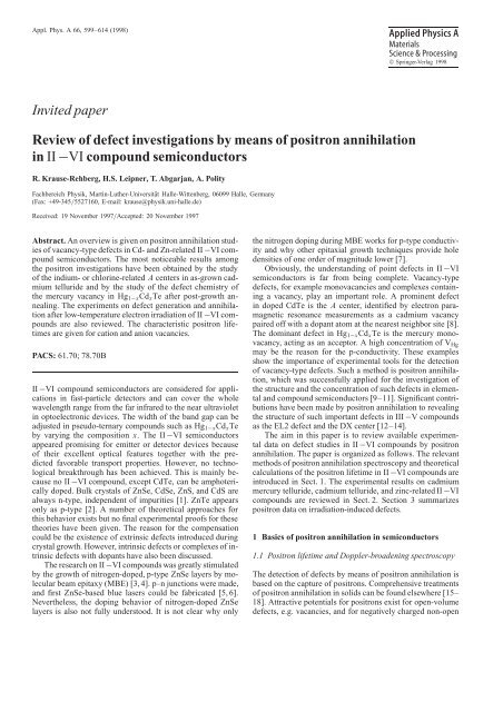
1200 ◦ C was investigated. The results <strong>of</strong> annealing experi-
Fig. 11. Doppler-broadening S parameter versus the annealing temperature<br />
measured in zinc oxide varistor ceramics [84]. Different cooling<br />
regimes were applied (air and furnace cooled, respectively). The regions<br />
I, II, and III are explained in the text<br />
ments are shown in Fig. 11. The appearance <strong>of</strong> the three<br />
distinct regions can be well understood in the framework<br />
<strong>of</strong> the supposed model [82]. The formation <strong>of</strong> Zn interstitials<br />
accompanied <strong>by</strong> the formation <strong>of</strong> negatively charged<br />
Zn vacancies near grain boundaries was anticipated in region<br />
I (Fig. 11). The increase in the S parameter as well as<br />
the increase in the photocurrent was taken as a pro<strong>of</strong> <strong>of</strong> the<br />
occurrence <strong>of</strong> both <strong>defect</strong>s. The decrease in region II was<br />
related to the enhanced diffusivity <strong>of</strong> oxygen and to the reaction<br />
<strong>of</strong> oxygen with the point <strong>defect</strong>s formed in region<br />
I. The further increase in the S parameter beyond 800 ◦ C<br />
(region III) was interpreted as either the thermal decomposition<br />
<strong>of</strong> ZnO or the generation <strong>of</strong> Frenkel pairs. The S<br />
parameter was a function <strong>of</strong> the cooling rate after annealing.<br />
The quenched air-cooled samples exhibited a lower S parameter<br />
than the furnace-cooled samples (Fig. 11). This fact<br />
was taken as a pro<strong>of</strong> that indeed point <strong>defect</strong>s near grain<br />
boundaries were examined.<br />
The sintering <strong>of</strong> ZnO ceramics has also been studied<br />
in more recent <strong>investigations</strong> [85–87] <strong>by</strong> <strong>positron</strong> annihilation<br />
and cathodoluminescence. No correlation could be<br />
established between the <strong>defect</strong>s acting as <strong>positron</strong> traps and<br />
luminescence centers. Doping with Mn, changing the conductivity<br />
from n-type to semiinsulating, did not alter the<br />
<strong>positron</strong> trapping significantly [85]. The change in <strong>positron</strong><br />
parameters was studied as a function <strong>of</strong> the sintering time<br />
and temperature. A <strong>defect</strong>-related lifetime <strong>of</strong> 255 ps was<br />
found after the ZnO was sintered at 1200 ◦ C. It was ascribed<br />
to <strong>defect</strong> complexes involving Zn vacancies. The<br />
experimentally obtained lifetime attained the bulk lifetime<br />
<strong>of</strong> 183 ps after the same sintering conditions. Similarly, an<br />
average <strong>positron</strong> lifetime <strong>of</strong> 180 ps was given <strong>by</strong> de la Cruz<br />
et al. [88] for untreated, high-resistivity as-grown ZnO, in<br />
contrast to a bulk lifetime <strong>of</strong> 169 ps reported after thermochemical<br />
reduction.<br />
3 Irradiation-induced <strong>defect</strong>s<br />
3.1 Cd-related II −VI compounds<br />
609<br />
An early <strong>positron</strong> annihilation study on irradiation-induced<br />
<strong>defect</strong>s in II −VI compounds was carried out <strong>by</strong> Moser et<br />
al. [89]. Electron irradiation experiments were performed at<br />
20 K with 3-MeV electrons to a dose <strong>of</strong> 1 × 10 18 cm −2 .Anannealing<br />
stage in the average <strong>positron</strong> lifetime was observed<br />
at 130 K for undoped CdTe. It was attributed to the annihilation<br />
<strong>of</strong> Frenkel pairs in both sublattices. Indium doping did<br />
not distinctly alter this annealing behavior. The same annealing<br />
stage was ascribed in a <strong>paper</strong> <strong>of</strong> Geffroy et al. [68] to<br />
the annealing <strong>of</strong> VCd. The <strong>defect</strong>-related <strong>positron</strong> lifetime was<br />
given as 330 ps, which is close to the value for the cadmium<br />
vacancy as part <strong>of</strong> the A center [52].<br />
Sen-Gupta and Moser [90] performed correlated Dopplerbroadening<br />
and <strong>positron</strong> lifetime measurements <strong>of</strong> undoped<br />
and In-doped CdTe in a temperature range from 20 to 70 K<br />
after electron irradiation (2.5MeV, 4×10 18 cm −2 , 20 K).<br />
A weak annealing stage was found at 50 K in correlation with<br />
PL results [91] obtained on the same specimens.<br />
Extended <strong>positron</strong> <strong>investigations</strong> on electron-irradiationinduced<br />
<strong>defect</strong>s in II −VI semiconductors were carried out<br />
<strong>by</strong> Polity et al. [92]. The annealing curve <strong>of</strong> a p-type<br />
CdTe sample irradiated at 4K with 2-MeV electrons (dose<br />
1 × 10 18 cm −2 ) is shown in Fig. 12a. The samples were kept<br />
at 77 K and mounted into the cryostat without intermediate<br />
warm-up. The <strong>positron</strong> lifetime was measured at 90 K after<br />
every annealing step and at 300 K after the annealing at room<br />
temperature. Three distinct ranges can be separated. A pronounced<br />
annealing stage is observed in the temperature range<br />
below 130 K, similar to the results <strong>of</strong> Moser et al. [89]. The<br />
second range comprises the increase in the average <strong>positron</strong><br />
lifetime between 130 and 170 K. The lifetime reaches the<br />
value measured prior to irradiation in the third range up to<br />
600 K.<br />
The correlated Hall effect measurements <strong>of</strong> the investigated<br />
p-type CdTe sample provided a Fermi-level position at<br />
EF − Ev = (215 ± 25) meV, which did not change noticeably<br />
Average <strong>positron</strong> lifetime [ps]<br />
300<br />
295<br />
290<br />
285<br />
280<br />
Measurement temperature<br />
90 K<br />
300 K<br />
() a<br />
287<br />
285<br />
283<br />
281<br />
279<br />
277<br />
Annealed at<br />
230 K<br />
330 K<br />
450 K<br />
570 K<br />
630 K<br />
Reference<br />
0 200 400 600 0 200 400 600<br />
Annealing temperature [K] Sample temperature [K]<br />
Fig. 12a,b. Positron-lifetime measurements <strong>of</strong> p-type cadmium telluride<br />
irradiated with 2-MeV electrons at 4K to a dose <strong>of</strong> 1 × 1018 cm−2 [92].<br />
a Average <strong>positron</strong> lifetime versus the annealing temperature. The measurement<br />
temperatures were 90 and 300 K, respectively. b Average <strong>positron</strong><br />
lifetime as a function <strong>of</strong> the temperature after several annealing steps<br />
(open symbols). The curve <strong>of</strong> a non-irradiated reference sample annealed<br />
at 570 K is added for comparison (closed circles)<br />
( b)
610<br />
after irradiation. The electrical measurements could be carried<br />
out, however, only after the room-temperature annealing<br />
step. Thus, the position <strong>of</strong> the Fermi level in the intermediate<br />
temperature range from 4 to 300 K remains unknown. There<br />
are two cases to be discussed. In case (i), the Fermi level stays<br />
above the 0/+ ionization level <strong>of</strong> the Te vacancy, i.e. <strong>positron</strong><br />
trapping in the neutral Te vacancies may be expected during<br />
the whole annealing procedure. In case (ii), the position <strong>of</strong> the<br />
Fermi level is temporarily shifted below the ionization level<br />
<strong>of</strong> the Te vacancy and moves up as a result <strong>of</strong> <strong>defect</strong> annealing<br />
to the value measured at room temperature, i.e. the Te vacancies<br />
are not detectable in this case because <strong>of</strong> their positive<br />
charge.<br />
The three annealing ranges are discussed at first under<br />
the assumption <strong>of</strong> the detectability <strong>of</strong> neutral Te vacancies,<br />
case (i). The average lifetime measured in the as-irradiated<br />
stage indicates the presence <strong>of</strong> vacancy-type <strong>defect</strong>s. After<br />
room-temperature annealing, τ reaches the value measured<br />
before irradiation, indicating the disappearance <strong>of</strong> both the<br />
Te and the Cd vacancies. This annealing also becomes apparent<br />
in Fig. 12b, where the average <strong>positron</strong> lifetime measured<br />
after several annealing steps is plotted as a function <strong>of</strong><br />
the sample temperature. The curves after annealing at 570<br />
and 630 K practically coincide with the curve <strong>of</strong> the nonirradiated<br />
reference sample, also annealed at 570 K.<br />
The recombination <strong>of</strong> Frenkel pairs in both sublattices<br />
is superimposed <strong>by</strong> the distinct maximum in τ at 170 K.<br />
This maximum might be due to the clustering <strong>of</strong> vacancies.<br />
It would lead to an increase in the <strong>defect</strong>-related lifetime.<br />
Unfortunately, the lifetime spectra could not be reliably decomposed<br />
to prove this fact. Under the assumption that all<br />
vacancies are clustered with no loss due to annealing, the<br />
trapping rate should remain constant according to (2) and the<br />
average lifetime should increase. This case is however not<br />
probable, because part <strong>of</strong> the vacancies are annealing.<br />
Thus, it is more likely that the maximum is due to the<br />
annealing <strong>of</strong> shallow <strong>positron</strong> traps. The average lifetime increases<br />
in this case, since competitive <strong>positron</strong> traps with<br />
a low <strong>defect</strong>-related lifetime vanish. Such shallow <strong>positron</strong><br />
traps may be irradiation-induced negatively charged intrinsic<br />
<strong>defect</strong>s, such as interstitials or antisites.<br />
Case (ii), i.e. the temporary appearance <strong>of</strong> positively<br />
charged Te vacancies, is discussed in the following. The first<br />
annealing stage is, under this assumption, due to the recombination<br />
<strong>of</strong> Frenkel pairs in the Cd sublattice. In addition to<br />
the explanation <strong>of</strong> the observed maximum given for case (i),<br />
a further possibility must be considered now. A +/0 charge<br />
transition <strong>of</strong> the Te vacancies may occur as a result <strong>of</strong> the shift<br />
<strong>of</strong> the Fermi level during annealing up to room temperature.<br />
The maximum may then correspond to the fact that the Te<br />
vacancies become visible for <strong>positron</strong>s.<br />
It is useful to include the results obtained in electronirradiated<br />
Hg1−xCdxTe with x = 0.2, 0.3, and 0.55 [92] for<br />
the discussion <strong>of</strong> cases (i) and (ii). The irradiation parameters<br />
were identical to the treatment <strong>of</strong> the CdTe sample described<br />
above. Only the results <strong>of</strong> the Hg0.45Cd0.55Te sample are exemplarily<br />
described here (Fig. 13). The other samples showed<br />
a similar behavior. The course <strong>of</strong> the average <strong>positron</strong> lifetime<br />
during the annealing experiment is plotted in Fig. 13a.<br />
The first annealing stage found in CdTe is also clearly visible<br />
in Hg1−xCdxTe for x = 0.2, but hardly detectable for x = 0.3<br />
and 0.55. However, the pronounced maximum at 250 K in the<br />
Positron lifetime [ps]<br />
350<br />
325<br />
300<br />
275<br />
310<br />
300<br />
290<br />
280<br />
� 2<br />
Sample<br />
temperature<br />
90 K<br />
300 K<br />
�−<br />
Average <strong>positron</strong> lifetime [ps]<br />
310 Annealing<br />
temperature<br />
300<br />
290<br />
230 K<br />
330 K<br />
450 K<br />
570 K<br />
280<br />
270<br />
() a<br />
270<br />
( b)<br />
100 300 500<br />
Annealing temperature [K]<br />
100 300 500<br />
Sample temperature [K]<br />
Fig. 13a,b. Positron-lifetime measurement <strong>of</strong> Hg0.45Cd0.55Te irradiated at<br />
4K with 2-MeV electrons to a dose <strong>of</strong> 1 × 10 18 cm −2 [92]. a Average<br />
<strong>positron</strong> lifetime τ and <strong>defect</strong>-related lifetime τ2 versus the annealing<br />
temperature. b Average <strong>positron</strong> lifetime as a function <strong>of</strong> the sample temperature<br />
measured after several annealing steps<br />
average <strong>positron</strong> lifetime occurs similar to the case <strong>of</strong> CdTe in<br />
all investigated Hg1−xCdxTe samples. Our favored interpretation,<br />
which is also supported <strong>by</strong> the results <strong>of</strong> Kiessling et al.<br />
[93], is the annealing <strong>of</strong> shallow <strong>positron</strong> traps in this range.<br />
The appearance <strong>of</strong> the maximum is thus similar to case (i)<br />
discussed above for CdTe.<br />
A two-component decomposition <strong>of</strong> the <strong>positron</strong> lifetime<br />
spectra was possible below 350 K annealing temperature in<br />
electron-irradiated Hg1−xCdxTe [92]. The second lifetime τ2<br />
equals 303 ps and 317 ps below and above the 200 K annealing<br />
temperature, respectively. This result can be understood<br />
under the assumption that the annealing <strong>of</strong> shallow <strong>positron</strong><br />
traps is the reason for the maximum in τ . The <strong>defect</strong>-related<br />
lifetime is always too small in a two-component decomposition<br />
in the presence <strong>of</strong> shallow traps, as shown <strong>by</strong> Monte<br />
Carlo simulation <strong>of</strong> <strong>positron</strong> lifetime spectra [94].<br />
The <strong>defect</strong>-related lifetime observed above 200 K lies in<br />
between those for a vacancy in the Hg/Cd sublattice and<br />
for a Te vacancy. The lifetime <strong>of</strong> a Hg vacancy amounts to<br />
305 ps, as described in Sect. 2.2. A lifetime <strong>of</strong> 323± 5pswas<br />
experimentally found for the Te vacancy [93]. The Fermi<br />
level was found to be shifted upwards after low-temperature<br />
electron irradiation, and the samples were heavily n-type [95].<br />
It was concluded that the Te vacancies are responsible for<br />
the Fermi-level pinning. In this case, vacancies in both sublattices<br />
are detectable. This is the main difference to the<br />
vacancy generation in Hg1−xCdxTe during post-growth annealing<br />
(see Sect. 2.2.1), where the Fermi level is determined<br />
<strong>by</strong> the acceptor-type Hg vacancies, and Te vacancies are positively<br />
charged and thus invisible for <strong>positron</strong>s.<br />
The results <strong>of</strong> the <strong>positron</strong> lifetime measurements performed<br />
as a function <strong>of</strong> temperature after certain annealing<br />
steps are shown in Fig. 13b [92]. No influence <strong>of</strong> shallow<br />
<strong>positron</strong> traps is visible in the low-temperature range after<br />
these annealing steps. This is in accordance with the interpretation<br />
<strong>of</strong> the observed maximum given above as the annealing<br />
<strong>of</strong> shallow traps below 200 K. On the other hand, the curves<br />
measured after annealing at 230 K and 330 K show the typi-
cal behavior for negatively charged vacancy-type <strong>defect</strong>s with<br />
the steep decrease in τ with increasing temperature. This behavior<br />
is most likely caused <strong>by</strong> the existence <strong>of</strong> negatively<br />
charged Hg vacancies, since the Te vacancies are neutral.<br />
However, average lifetimes distinctly above the <strong>defect</strong>-related<br />
lifetime <strong>of</strong> the Hg vacancy were reported in another annealing<br />
study <strong>of</strong> electron-irradiated Hg0.78Cd0.22Te <strong>by</strong> Kiessling<br />
et al. [93]. A <strong>defect</strong>-related lifetime <strong>of</strong> 323 ps was observed<br />
and was attributed to <strong>positron</strong> trapping in Te vacancies. Combining<br />
the results <strong>of</strong> Polity et al. [92] and Kiessling et al. [93],<br />
it may be concluded that actually a mixture <strong>of</strong> Hg and Te<br />
vacancies is observed.<br />
To summarize the results obtained in low-temperature<br />
electron-irradiated CdTe and Hg1−xCdxTe, we can say that<br />
the annealing behavior is very similar. The annealing <strong>of</strong> the<br />
irradiation-induced vacancies in both sublattices occurs in the<br />
range from 100 to 400 K leading to a decrease in the average<br />
<strong>positron</strong> lifetime. The observed maximum between 150<br />
and 250 K is likely to be due to the superimposed increase <strong>of</strong><br />
τ as a result <strong>of</strong> the annealing <strong>of</strong> irradiation-induced shallow<br />
<strong>positron</strong> traps.<br />
There have been only two <strong>positron</strong> studies on ion implantation<br />
in Cd-related II −VI compounds [96, 97]. Liszkay et<br />
al. [96] studied Hg0.78Cd0.22Te implanted with 320 keV Al<br />
ions at 100 and 300 K. The <strong>defect</strong>-related Doppler parameters<br />
were found to be Sd/Sb = 1.05 and Wd/Wb = 0.8. A previous<br />
study <strong>of</strong> Hg monovacancies in this material gave a value <strong>of</strong><br />
Sd/Sb = 1.02 [98]. Hence, Liszkay et al. concluded the existence<br />
<strong>of</strong> implantation-induced small vacancy clusters, at least<br />
<strong>of</strong> the size <strong>of</strong> divacancies. The formation <strong>of</strong> vacancy agglomerates<br />
was also reported <strong>by</strong> Voitsekhovskii et al. [97]. The divacancy<br />
generation reached a saturation at room temperature<br />
with a density <strong>of</strong> 4 × 10 16 cm −3 at a dose <strong>of</strong> 3 × 10 12 cm −2 ,<br />
whereas after implantation at 100 K the divacancy density exceeded<br />
1 × 10 18 cm −3 [96].<br />
3.2 Zn-related II −VI compounds<br />
In practically all studies <strong>of</strong> <strong>defect</strong> formation after lowtemperature<br />
electron irradiation in Zn-related semiconductors,<br />
the Zn vacancies are supposed to be single or double<br />
negatively charged, whereas the anion vacancies are assumed<br />
to be positively charged. As a consequence, only the Zn vacancies<br />
are detectable <strong>by</strong> <strong>positron</strong> annihilation.<br />
The first <strong>positron</strong> study on Zn-related II −VI compounds<br />
was carried out <strong>by</strong> Moser et al. [89] for ZnTe irradiated at<br />
20 K with 1 × 10 18 cm −2 , 3-MeV electrons. A main annealing<br />
stage appeared at 500 K.<br />
The average <strong>positron</strong> lifetime was measured in ZnSe<br />
electron-irradiated at 4K(2MeV,1×10 18 cm −2 ) <strong>by</strong> Abgarjan<br />
[99]. The results are compared to a sample irradiated<br />
with 200-MeV Ne ions at room temperature to a dose <strong>of</strong><br />
1 × 10 14 cm −2 (Fig. 14). A continuous increase in the average<br />
lifetime was found in the electron-irradiated sample up<br />
to 300 K. The increase was discussed as resulting from either<br />
vacancy clustering or the annealing <strong>of</strong> shallow <strong>positron</strong> traps<br />
[99]. A <strong>defect</strong>-related component <strong>of</strong> 300 to 310 ps could be<br />
resolved. It can be concluded from the comparison with the<br />
theoretical calculations (Table 1) that this component may be<br />
due to a divacancy or a divacancy-related complex as supposed<br />
<strong>by</strong> Pareja et al. [79]. The case <strong>of</strong> the annealing <strong>of</strong><br />
611<br />
shallow traps can be excluded with these results, because<br />
a comparable increase in τ was found both for low and high<br />
sample temperatures.<br />
The ZnSe sample irradiated at room temperature with Ne<br />
ions also exhibited a slight increase in the average lifetime up<br />
to 450 K (Fig. 14). Because the same <strong>defect</strong>-related lifetime<br />
<strong>of</strong> 300 to 310 ps was resolved, and the main annealing stage<br />
was also observed between 500 and 700 K, it was concluded<br />
that the same <strong>defect</strong> types dominated the <strong>positron</strong> trapping in<br />
the electron-irradiated and in the Ne-irradiated samples.<br />
In contrast to Abgarjan [99], Pareja et al. [79] found in the<br />
temperature range between 77 and 125 K an annealing stage<br />
that was interpreted as the recombination <strong>of</strong> close Frenkel<br />
pairs in the Zn sublattice. Another difference was the temperature<br />
dependence <strong>of</strong> the <strong>positron</strong> lifetime. Abgarjan measured<br />
an increase <strong>of</strong> about 5ps <strong>by</strong> cooling the sample from<br />
room temperature to 100 K. However, a distinct decrease<br />
was observed <strong>by</strong> Pareja et al. [79] in the same temperature<br />
range and was related to the charge-state transition <strong>of</strong> the<br />
divacancy-type <strong>defect</strong>s possibly not appearing in the samples<br />
<strong>of</strong> a different supplier used <strong>by</strong> Abgarjan [99].<br />
The <strong>positron</strong> lifetime was measured <strong>by</strong> Pareja et al. also<br />
in ZnS after electron irradiation at 20 and 77 K [79]. The<br />
initial annealing stage <strong>of</strong> close Frenkel pairs observed in<br />
ZnSe was not observed at the lowest measuring temperature<br />
<strong>of</strong> about 80 K. The average <strong>positron</strong> lifetime increased<br />
from 240 to 280 ps during the annealing procedure up to<br />
700 K. A similar annealing stage to that in ZnSe was not<br />
Average lifetime [ps]<br />
270<br />
260<br />
250<br />
240<br />
270<br />
260<br />
250<br />
240<br />
Measured at 100 K<br />
e �<br />
2 MeV<br />
1�10 cm<br />
18 2 �<br />
Measured at 300 K<br />
Ne +<br />
200 MeV<br />
1�10 cm<br />
14 2 �<br />
200 400 600 800<br />
Annealing temperature [K]<br />
Fig. 14. Annealing experiment <strong>of</strong> electron-irradiated zinc selenide (2MeV,<br />
1×10 18 cm −2 , 4K) compared to ZnSe crystals irradiated with neon ions<br />
(200 MeV, 1 × 10 14 cm −2 , 300 K). The <strong>positron</strong> lifetime was measured at<br />
100 K in the electron-irradiated sample and at 300 K in the Ne + -irradiated<br />
sample [99]
612<br />
found in ZnS up to this temperature. The increase in τ<br />
was attributed to VZn-related <strong>defect</strong>s. It was observed that<br />
the <strong>defect</strong>-related lifetime <strong>of</strong> a sample irradiated at room<br />
temperature decreased with decreasing temperature below<br />
300 K [100]. This effect was interpreted as the change <strong>of</strong><br />
the charge state <strong>of</strong> the irradiation-induced vacancy-type <strong>defect</strong>s<br />
rather than the appearance <strong>of</strong> shallow <strong>positron</strong> traps.<br />
However, electrical measurements are desirable for the confirmation<br />
<strong>of</strong> this interpretation.<br />
Electron-irradiated ZnO crystals were investigated <strong>by</strong><br />
Tomiyama et al. [101]. The irradiation conditions were<br />
28 MeV, 4 × 10 18 cm −2 ,and77 K. A clear annealing stage<br />
was found at 450 K. The interpretation given for this stage<br />
as the disappearance <strong>of</strong> irradiation-induced oxygen monovacancies<br />
seems to be unlikely, since these <strong>defect</strong>s are expected<br />
to be positively charged [102]. The annealing behavior was<br />
found to be completely different after irradiation with 3-MeV<br />
protons at 223 K. A <strong>defect</strong>-related lifetime <strong>of</strong> 273 ps was<br />
separated after this irradiation (Fig. 15). It was attributed to<br />
divacancies, because the τd/τb ratio reached 1.48. In contrast,<br />
this ratio was 1.15 after low-temperature electron irradiation,<br />
corresponding to a monovacancy-related lifetime <strong>of</strong><br />
211 ps. The measured average <strong>positron</strong> lifetime, as well as<br />
the Doppler-broadening S parameter increased during subsequent<br />
annealing in the temperature range <strong>of</strong> 300 to 550 ◦ C.As<br />
the <strong>defect</strong>-related lifetime τ2 increased in the same temperature<br />
range up to 378 ps, it was concluded that the divacancies<br />
Fig. 15. Positron-annihilation measurements <strong>of</strong> an annealing experiment <strong>of</strong><br />
a zinc oxide single crystal irradiated with 3-MeV protons at 223 K [102].<br />
The lifetime components τ1 (◦) andτ2 ( ) <strong>of</strong> a two-component spectra<br />
decomposition are shown in the upper panel. The average <strong>positron</strong> lifetime<br />
( ) and the Doppler-broadening S parameter (×) are plotted in the lower<br />
panel<br />
grow further to larger agglomerates. These agglomerates annealed<br />
during subsequent heat treatment, and the average<br />
<strong>positron</strong> lifetime approached the bulk lifetime at 1100 ◦ C.<br />
4 Summary<br />
Vacancy-related <strong>defect</strong>s may play an important role for many<br />
<strong>of</strong> the electrical and optical properties <strong>of</strong> II −VI compound<br />
semiconductors. Positron annihilation is a specific method for<br />
the investigation <strong>of</strong> the concentration and the kind <strong>of</strong> these<br />
<strong>defect</strong>s. The <strong>defect</strong>-related <strong>positron</strong> lifetime especially provides<br />
information on the size <strong>of</strong> the open-volume <strong>defect</strong>, i.e.<br />
it can be distinguished between monovacancies, divacancies,<br />
and larger agglomerates. Furthermore, the temperature dependence<br />
<strong>of</strong> the <strong>positron</strong> trapping may give indications on the<br />
charge state <strong>of</strong> the vacancies. The comparison <strong>of</strong> Dopplerbroadening<br />
measurements with theoretical calculations in the<br />
high-momentum part may allow in the future the identification<br />
<strong>of</strong> the chemical surrounding <strong>of</strong> the vacancy, and hence<br />
the identification <strong>of</strong> the corresponding sublattice <strong>of</strong> the <strong>defect</strong>.<br />
However, it is still rather difficult to analyze whether the<br />
vacancy is isolated or part <strong>of</strong> a complex with an impurity or<br />
another intrinsic <strong>defect</strong>.<br />
The <strong>positron</strong> studies <strong>of</strong> <strong>defect</strong>s in II −VI compounds have<br />
been reviewed in this <strong>paper</strong>. Defects in the as-grown state,<br />
after heat treatment, and after low-temperature irradiation<br />
have been dealt with. The main emphasis <strong>of</strong> the <strong>investigations</strong><br />
was put on the characterization <strong>of</strong> Cd-related compounds. Important<br />
results were obtained from the investigation <strong>of</strong> the<br />
A centers in indium- and chlorine-doped cadmium telluride<br />
and from the quantitative analysis <strong>of</strong> the <strong>defect</strong> chemistry in<br />
Hg1−xCdxTe crystals related to the mercury vacancy.<br />
As the <strong>positron</strong>s are very sensitive to the charge state <strong>of</strong><br />
the detected vacancy, a reliable interpretation <strong>of</strong> the data requires<br />
the knowledge <strong>of</strong> the position <strong>of</strong> the Fermi level to be<br />
determined from electrical measurements. Furthermore, such<br />
<strong>positron</strong> experiments were especially successful with respect<br />
to the <strong>defect</strong> identification, when other <strong>defect</strong>-sensitive techniques<br />
were applied to the same samples. Future progress<br />
can also be expected from the improvement <strong>of</strong> the theoretical<br />
calculations <strong>of</strong> the ionization levels <strong>of</strong> the <strong>defect</strong>s and the<br />
determination <strong>of</strong> <strong>defect</strong>-related <strong>positron</strong> lifetimes, taking into<br />
account the lattice relaxation.<br />
References<br />
1. S.S. Devlin: In Physics and Chemistry <strong>of</strong> II −VI Compounds, ed. <strong>by</strong><br />
A. Aven, J.S. Prener (North-Holland, Amsterdam 1967) p. 551<br />
2. J.L. Pautrat, J.M. Francou, N. Magnea, E. Molva, K. Saminadayar:<br />
J. Cryst. Growth 72, 194 (1985)<br />
3. A. Taike, M. Migita, H. Yamamoto: Appl. Phys. Lett. 56, 1989 (1990)<br />
4. R.M. Park, M.B. Tr<strong>of</strong>fer, C.M. Rouleau, J.M. DePuydt, M.A. Haase:<br />
Appl. Phys. Lett. 57, 2127 (1990)<br />
5. K. Ohkawa, T. Karasawa, T. Mitsuyu: J. Cryst. Growth 111, 797<br />
(1991)<br />
6. M.A. Haase, Y. Qiu, J.M. DePuydt, H. Cheng: Appl. Phys. Lett. 59,<br />
1272 (1991)<br />
7. A. Ohki, Y. Kawaguchi, K. Ando, A. Katsui: Appl. Phys. Lett. 59, 671<br />
(1991)<br />
8. D.M. H<strong>of</strong>mann, P. Omling, H.G. Grimmeiss, B.K. Meyer, K.W. Benz,<br />
D. Sinerius: Phys. Rev. B 45, 6247 (1992)
9. G. Dlubek, R. Krause: Phys. Stat. Sol. (a) 102, 443 (1987)<br />
10. P. Asoka-Kumar, K.G. Lynn, D.O. Welch: J. Appl. Phys. 76, 4935<br />
(1994)<br />
11. P. Hautojärvi, C. Corbel: In Positron Spectroscopy <strong>of</strong> Solids, ed. <strong>by</strong><br />
A. Dupasquier, J.A.P. Mills (IOS Press, Amsterdam 1995) p. 491<br />
12. R. Krause, K. Saarinen, P. Hautojärvi, A. Polity, G. Gärtner, C. Corbel:<br />
Phys. Rev. Lett. 65, 3329 (1990)<br />
13. R. Krause-Rehberg, T. Drost, A. Polity, G. Roos, G. Pensl, D. Volm,<br />
B.K. Meyer, G. Bischopink, K.W. Benz: Phys. Rev. B 48, 11723<br />
(1993)<br />
14. J. Mäkinen, T. Laine, K. Saarinen, P. Hautojärvi, C. Corbel, V.M. Airaksinen,<br />
P. Gibart: Phys. Rev. Lett. 71, 3154 (1993)<br />
15. P. Hautojärvi (Ed.): Positrons in solids (Springer, Berlin, Heidelberg<br />
1979)<br />
16. W. Brandt, A. Dupasquier (Eds.): Positron Solid State Physics (North<br />
Holland, Amsterdam 1981)<br />
17. A. Dupasquier, J.A.P. Mills (Eds.): Positron Spectroscopy <strong>of</strong> Solids<br />
(IOS Press, Amsterdam 1995)<br />
18. M.J. Puska, R.M. Nieminen: Rev. Mod. Phys. 66, 841 (1994)<br />
19. K. Saarinen, P. Hautojärvi, A. Vehanen, R. Krause, G. Dlubek: Phys.<br />
Rev. B 39, 5287 (1989)<br />
20. L. Liszkay, C. Corbel, L. Baroux, P. Hautojärvi, M. Bayhan, A.W. Brinkmann,<br />
S. Tatarenko: Appl. Phys. Lett. 64, 1380 (1994)<br />
21. M. Clement, J.M.M. de Nijs, P. Balk, H. Schut, A. van Veen: J. Appl.<br />
Phys. 79, 9029 (1996)<br />
22. P.J. Schultz, K.G. Lynn: Rev. Mod. Phys. 60, 701 (1988)<br />
23. A. Dupasquier, G. Ottaviani: In Positron Spectroscopy <strong>of</strong> Solids, ed. <strong>by</strong><br />
A. Dupasquier, J.A.P. Mills (IOS Press, Amsterdam 1995) p. 581<br />
24. R. Krause-Rehberg, H.S. Leipner: Appl. Phys. A 64, 457 (1997)<br />
25. R.M. Nieminen, J. Laakkonen: Appl. Phys. 20, 181 (1979)<br />
26. M.J. Puska, C. Corbel, R.M. Nieminen: Phys. Rev. B 41, 9980 (1990)<br />
27. J. Mäkinen, P. Hautojärvi, C. Corbel: J. Phys. Cond. Mat. 4, 5137<br />
(1992)<br />
28. C. Le Berre, C. Corbel, K. Saarinen, S. Kuisma, P. Hautojärvi, R. Fornari:<br />
Phys. Rev. B 52, 8112 (1995)<br />
29. M. Manninen, R.M. Nieminen: Appl. Phys. A 26, 93 (1981)<br />
30. M. Berlotaccini, A. Dupasquier: Phys. Rev. B 1, 2896 (1970)<br />
31. W. Brandt, R. Paulin: Phys. Rev. B 5, 2430 (1972)<br />
32. W. Frank, A. Seeger: Appl. Phys. 3, 66 (1974)<br />
33. M.J. Puska: Mater. Sci. Forum 10-12, 277 (1986)<br />
34. F. Plazaola, A.P. Seitsonen, M.J. Puska: J. Phys. Cond. Mat. 6, 8809<br />
(1994)<br />
35. F. Plazaola, A.P. Seitsonen, M.J. Puska: Mater. Sci. Forum 175-178,<br />
469 (1995)<br />
36. M.J. Puska, R.M. Nieminen: J. Phys. F 13, 333 (1983)<br />
37. E. Boronski, R.M. Nieminen: Phys. Rev. B 34, 3820 (1986)<br />
38. M.J. Puska, S. Mäkinen, M. Manninen, R.M. Nieminen: Phys. Rev. B<br />
39, 7666 (1989)<br />
39. P.H. Kasai, Y. Otomo: J. Chem. Phys. 37, 1263 (1962)<br />
40. J.W. Allen: Semicond. Sci. Technol. 10, 1049 (1995)<br />
41. K. Zanio: Semicond. Semimet. 13, 129 (1972)<br />
42. P. Emanuelsson, P. Omling: Phys. Rev. B 47, 15578 (1993)<br />
43. B.K. Meyer, P. Omling, E. Weigel, G. Müller-Vogt: Phys. Rev. B 46,<br />
15135 (1992)<br />
44. C. Gély, C. Corbel, R. Triboulet: Comptes Rendus de l’Academie des<br />
Sciences Serie II 309, 179 (1989)<br />
45. C. Gély-Sykes, C. Corbel, R. Triboulet: Sol. State Comm. 80, 79<br />
(1991)<br />
46. C. Corbel, L. Baroux, F.M. Kiessling, C. Gely-Sykes, R. Triboulet:<br />
Mater. Sci. Eng. B 16, 134 (1993)<br />
47. F. Fischer, A. Waag, L. Worschech, W. Ossau, S. Scholl, G. Landwehr,<br />
J. Mäkinen, P. Hautojärvi, C. Corbel: J. Cryst. Growth 161, 214 (1996)<br />
48. H. Kauppinen, L. Baroux: J. Phys. Cond. Mat. 9, 5495 (1997)<br />
49. K.G. Lynn, J.R. MacDonald, R.A. Boie, L.C. Feldman, J.D. Gabbe,<br />
M.F. Robbins, E. Bonderup, J. Golovchenko: Phys. Rev. Lett. 38, 241<br />
(1977)<br />
50. M. Alatalo, H. Kauppinen, K. Saarinen, M.J. Puska, J. Mäkinen,<br />
P. Hautojärvi, R.M. Nieminen: Phys. Rev. B 51, 4176 (1995)<br />
51. A. Polity, T. Abgarjan, R. Krause-Rehberg: Mater. Sci. Forum 175-<br />
178, 473 (1995)<br />
52. R. Krause-Rehberg, A. Polity, T. Abgarjan, W. Stadler, D.M. H<strong>of</strong>mann,<br />
B.K. Meyer, M. Azoulay: submitted to Phys. Rev. B (1998)<br />
53. H. Zimmermann, R. Boyn, P. Rudolph, J. Bollmann, A. Klimakow,<br />
R. Krause: Mater. Sci. Eng. B 16, 139 (1993)<br />
54. R. Krause-Rehberg, H. Zimmermann, A. Klimakow, T. Drost: Phys.<br />
613<br />
Stat. Sol. A 134, K45 (1992)<br />
55. E. Grillot, M. Bancie-Grillot, M. Egee: J. Lumin. 12, 461 (1976)<br />
56. A. Sher, M.A. Berding, M. van Schilfgaarde: Semicond. Sci. Technol.<br />
6, C59 (1991)<br />
57. C.E. Jones: J. Vac. Sci. Technol. A 3, 131 (1985)<br />
58. H.R. Vydyanath: J. Electrochem. Soc. 128, 2609 (1981)<br />
59. A.V. Voitsekhovskii, A.P. Kokhanenko, Y.V. Lilenko, A.D. Pogrebnyak,<br />
S.M. Ruzimov, R.D. Babadzhanov: Sov. Phys. Semicond. 20,<br />
514 (1986)<br />
60. I.Y. Dekhtyar, M.I. Dekhtyar, V.V. Dyakin, F.A. Zaitov, A.I. Vlasenko,<br />
S.P. Likhtorovich, A.A. Lyubchenko, S.G. Sakharova, V.I. Silant’ev,<br />
R.G. Fedchenko: Sov. Phys. Semicond. 18, 1230 (1984)<br />
61. G.Y. Andersen, V.V. Dyakin, F.A. Zaitov, V.V. Koval, A.V. Lyubchenko,<br />
V.I. Silant’ev, R.G. Fedchenko: Inorg. Mater. 23, 1149 (1987)<br />
62. H.R. Vydyanath, J.C. Donovan, D.A. Nelson: J. Electrochem. Soc.<br />
128, 2625 (1981)<br />
63. R. Krause, A. Polity, A. Klimakow, M. Schenk: In Positron Annihilation,<br />
ed. <strong>by</strong> L. Dorikens-Vanpraet, M. Dorikens, D. Segers (World<br />
Scientific, Singapore 1989) p. 684<br />
64. R. Krause, A. Klimakow, F.M. Kiessling, A. Polity, P. Gille, M. Schenk:<br />
J. Cryst. Growth 101, 512 (1990)<br />
65. M. Neubert, K. Jacobs, R. Krause-Rehberg, T. Abgarjan, P. Gille,<br />
W. Hoerstel: J. Appl. Phys. 79, 7563 (1996)<br />
66. R. Krause-Rehberg, T. Drost, A. Polity: Mater. Sci. Forum 143-147,<br />
429 (1994)<br />
67. R. Krause-Rehberg, T. Abgarjan, A. Polity, M. Neubert: Mater. Sci.<br />
Forum 196-201, 1285 (1995)<br />
68. B. Geffroy, C. Corbel, M. Stucky, R. Triboulet, P. Hautojärvi, F. Plazaola,<br />
K. Saarinen, H. Rajainmaki, J. Aaltonen, P. Moser, A. Sengupta,<br />
J.L. Pautrat: Mater. Sci. Forum 10-12, 1241 (1986)<br />
69. C. Gély, C. Corbel, R. Triboulet: J. Phys. Cond. Mat. 2, 4763 (1990)<br />
70. L. Baroux, C. Corbel, F.M. Kiessling, S. Rolland, R. Granger, W. Hoerstel,<br />
R. Triboulet: Phys. Rev. Lett. 75, 557 (1995)<br />
71. C. Smith, P.C. Rice-Evans, N. Shaw: AIP Conf. Proc. 303, 78 (1994)<br />
72. R. Krause, M. Neubert, T. Drost, W. Hoerstel, A. Polity, F.M. Kiessling,<br />
U. Paitz, V. Zlomanov, S. Mäkinen: Mater. Sci. Forum 105-110, 333<br />
(1992)<br />
73. T. Miyajima, L. Wei, S. Tanigawa, H. Okuyama, K. Akimoto, Y. Mori:<br />
Mater. Sci. Forum 105-110, 1423 (1992)<br />
74. L. Wei, C. Yang-Koo, C. Dosho, S. Tanigawa, T. Yodo, K. Yamashita:<br />
Jpn. J. Appl. Phys. Pt. 1 30, 2442 (1991)<br />
75. L. Liszkay, C. Corbel, P. Hautojärvi, R. Aulombard, T. Cloître, J. Griesche,<br />
F. Kiessling: Appl. Phys. Lett. 70, 2723 (1997)<br />
76. S. Dannefaer, D. Kerr: J. Appl. Phys. 60, 1313 (1986)<br />
77. K. Terashima, E. Tokizaki, A. Uedono, S. Tanigawa: Jpn. J. Appl.<br />
Phys., Part 1 32, 736 (1993)<br />
78. R. Pareja, R.M. de la Cruz: Phys. Stat. Sol. B 178, K23 (1993)<br />
79. R. Pareja, R.M. de la Cruz, P. Moser: J. Phys. Cond. Mat. 4, 7153<br />
(1992)<br />
80. M. Adams, P. Mascher, A.H. Kitai: Appl. Phys. A 61, 217 (1995)<br />
81. K. Saarinen, T. Laine, K. Skog, J. Mäkinen, P. Hautojärvi, K. Rakennus,<br />
P. Uusimaa, A. Salokatve, M. Pessa: Phys. Rev. Lett. 77, 3407<br />
(1996)<br />
82. T.K. Gupta, W.G. Carlson: J. Mater. Sci. 20, 3487 (1987)<br />
83. C. Hübner, T. Staab, R. Krause-Rehberg: Appl. Phys. A 61, 203 (1995)<br />
84. T.K. Gupta, W.D. Straub, M.S. Ramanachalam, J.P. Schaffer, A. Rohatgi:<br />
J. Appl. Phys. 66, 6132 (1989)<br />
85. P. Mascher, M. Liu, A.H. Kitai, W. Puff: Mater. Sci. Forum 105-110,<br />
1145 (1992)<br />
86. J. Zhong, A.H. Kitai, P. Mascher, W. Puff: J. Electrochem. Soc. 140,<br />
3644 (1993)<br />
87. J. Zhong, P. Mascher, W. Puff, A.H. Kitai: Mater. Sci. Forum 143-147,<br />
465 (1994)<br />
88. R.M. de la Cruz, R. Pareja, R. Gonzalez, L.A. Boatner, Y. Chen: Phys.<br />
Rev. B 45, 6581 (1992)<br />
89. P. Moser, J.L. Pautrat, C. Corbel, P. Hautojärvi: In Positron Annihilation,<br />
ed. <strong>by</strong> P.C. Jain, R.M. Singru, K.P. Gopinathan (World Scientific,<br />
Singapore 1985) p. 733<br />
90. A. Sen-Gupta, P. Moser: In Positron Annihilation, ed. <strong>by</strong> L. Dorikens-<br />
Vanpraet, M. Dorikens, D. Segers (World Scientific, Singapore 1989)<br />
p. 731<br />
91. E. Molva, J.L. Pautrat: Solid State Commun. 39, 1151 (1981)<br />
92. A. Polity, F. Rudolf, T. Abgarjan: unpublished results (1997)<br />
93. F.M. Kiessling, C. Corbel, L. Baroux, S. Rolland, R. Triboulet: Phys.<br />
Rev. B 52, 9925 (1995)
614<br />
94. B. Somieski, T.E.M. Staab, R. Krause-Rehberg: Nucl. Instrum. Methods.<br />
Phys. Res. A 381, 128 (1996)<br />
95. J. Favre, M. Konczykowski, C. Blanchard: Ann. Phys. 14, 193 (1989)<br />
96. L. Liszkay, C. Corbel, L. Baroux, P. Hautojärvi, A. Declemy, P.O. Renault:<br />
J. Phys. Cond. Mat. 7, 8529 (1995)<br />
97. A.V. Voitsekhovskii, A.G. Korotaev, A.P. Kokhanenko: Rus. Phys. J.<br />
38, 1007 (1995)<br />
98. C.D. Smith, P. Rice-Evans, N. Shaw: Phys. Rev. Lett. 72, 1108 (1994)<br />
99. T. Abgarjan: Thesis, Martin-Luther-Universität Halle 1994<br />
100. R.M. de la Cruz, R. Pareja, P. Moser: Mater. Sci. Forum 105-110, 957<br />
(1992)<br />
101. N. Tomiyama, M. Takenaka, E. Kuramoto: Mater. Sci. Forum 105-110,<br />
1281 (1992)<br />
102. W. Puff, S. Brunner, P. Mascher, A.G. Balogh: Mater. Sci. Forum 196-<br />
201, 333 (1995)<br />
103. T. Miyajima, H. Okuyama, K. Akimoto, Y. Mori, L. Wei, S. Tanigawa:<br />
Appl. Phys. Lett. 59, 1482 (1991)<br />
104. S. Dannefaer: J. Phys. C 15, 599 (1982)