ANALOG DIVIDER DIV100 - ClassicCMP
ANALOG DIVIDER DIV100 - ClassicCMP
ANALOG DIVIDER DIV100 - ClassicCMP

Create successful ePaper yourself
Turn your PDF publications into a flip-book with our unique Google optimized e-Paper software.
®<br />
<strong>DIV100</strong><br />
<strong>ANALOG</strong> <strong>DIVIDER</strong><br />
FEATURES<br />
● HIGH ACCURACY: 0.25% Maximum Error,<br />
40:1 Denominator Range<br />
● TWO-QUADRANT OPERATION<br />
Dedicated Log-Antilog Technique<br />
● EASY TO USE<br />
Laser-trimmed to Specified Accuracy<br />
No External Resistors Needed<br />
● LOW COST<br />
● DIP PACKAGE<br />
DESCRIPTION<br />
The <strong>DIV100</strong> is a precision two-quadrant analog<br />
divider offering superior performance over a wide<br />
range of denominator input. Its accuracy is nearly two<br />
orders of magnitude better than multipliers used for<br />
division. It consists of four operational amplifiers and<br />
logging transistors integrated into a single monolithic<br />
circuit and a laser-trimmed, thin-film resistor network.<br />
The electrical characteristics of these devices offer the<br />
user guaranteed accuracy without the need for external<br />
adjustment — the <strong>DIV100</strong> is a complete, single package<br />
analog divider.<br />
APPLICATIONS<br />
● DIVISION<br />
● SQUARE ROOT<br />
● RATIOMETRIC MEASUREMENT<br />
● PERCENTAGE COMPUTATION<br />
● TRANSDUCER AND BRIDGE<br />
LINEARIZATION<br />
● AUTOMATIC LEVEL AND GAIN CONTROL<br />
● VOLTAGE CONTROLLED AMPLIFIERS<br />
● <strong>ANALOG</strong> SIMULATION<br />
For those applications requiring higher accuracy than<br />
the <strong>DIV100</strong> specifies, the capability for optional<br />
adjustment is provided. These adjustments allow the<br />
user to set scale factor, feedthrough, and outputreferred<br />
offsets for the lowest total divider error.<br />
The <strong>DIV100</strong> also gives the user a precision, temperature-compensated<br />
reference voltage for external use.<br />
Designers of industrial process control systems,<br />
analytical instruments, or biomedical instrumentation<br />
will find the <strong>DIV100</strong> easy to use and also a low cost,<br />
but highly accurate solution to their analog divider<br />
applications.<br />
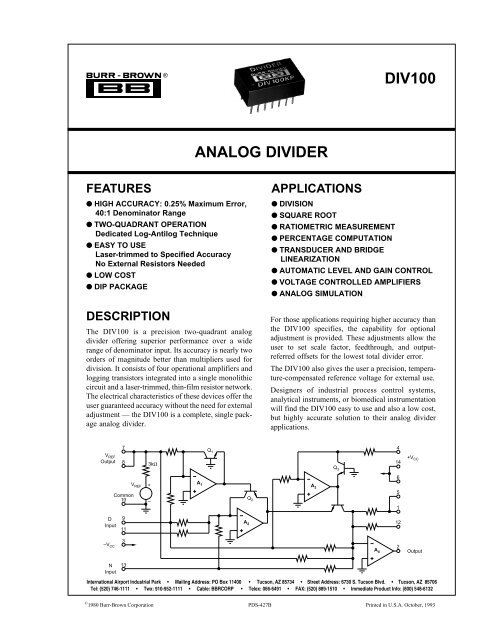
7<br />
Q 1<br />
4<br />
V REF<br />
Output<br />
8<br />
3kΩ<br />
<br />
Q 3<br />
14<br />
+V CC<br />
<br />
Common<br />
10<br />
V REF +<br />
–<br />
A 1<br />
Q 2<br />
<br />
A 3<br />
<br />
6<br />
5<br />
1<br />
D <br />
Input<br />
9<br />
11<br />
A 2<br />
12<br />
–V CC<br />
N<br />
Input<br />
3<br />
13<br />
A 4<br />
2<br />
Output <br />
<br />
International Airport Industrial Park • Mailing Address: PO Box 11400 • Tucson, AZ 85734 • Street Address: 6730 S. Tucson Blvd. • Tucson, AZ 85706<br />
Tel: (520) 746-1111 • Twx: 910-952-1111 • Cable: BBRCORP • Telex: 066-6491 • FAX: (520) 889-1510 • Immediate Product Info: (800) 548-6132<br />
© 1980 Burr-Brown Corporation PDS-427B Printed in U.S.A. October, 1993
SPECIFICATIONS<br />
ELECTRICAL<br />
At T A<br />
= +25°C and V CC<br />
= ±15VDC, unless otherwise specified.<br />
<strong>DIV100</strong>HP<br />
<strong>DIV100</strong>JP<br />
<strong>DIV100</strong>KP<br />
PARAMETER CONDITIONS MIN TYP MAX MIN TYP MAX MIN TYP MAX UNITS<br />
TRANSFER FUNCTION<br />
V O<br />
= 10N/D<br />
ACCURACY<br />
R L ≥ 10kΩ<br />
Total Error<br />
Initial 0.25V ≤ D ≤ 10V, N ≤ |D| 0.7 1.0 0.3 0.5 0.2 0.25 % FSO (1)<br />
vs Temperature 1V ≤ D ≤ 10V, N ≤ |D| 0.02 0.05 (2) * * * * % FSO/°C<br />
0.25V ≤ D ≤ 1V, N ≤ |D| 0.06 0.2 (2) * * * * % FSO/°C<br />
vs Supply 0.25V ≤ D ≤ 10V, N ≤ |D| 0.15 * * % FSO/%<br />
Warm-up TIme to Rated Performace 5 * * Minutes<br />
AC PERFORMANCE D = +10V<br />
Small-Signal Bandwidth –3dB 350 * * kHz<br />
0.5% Amplitude Error Small-Signal 15 * * kHz<br />
0.57° Vector Error Small-Signal 1000 * * Hz<br />
Full-Power Bandwidth V O = ±10V, I O = ±5mA 30 * * kHz<br />
Slew Rate V D = ±10V, I O = ±5mA 2 * * V/µs<br />
Settling Time ε = 1%, ∆V O = 20V 15 * * µs<br />
Overload Recovery 50% Output Overload 4 * * µs<br />
INPUT CHARACTERISTICS<br />
Input Voltage Range<br />
Numerator N ≤ |D| ±10 * * V<br />
Denominatior D ≥ +250mV ±10 * * V<br />
Input Resistance Either Input 25 * * kΩ<br />
OUTPUT CHARACTERISTICS<br />
Full-Scale Output ±10 * * V<br />
Rated Output<br />
Voltage I O = ±5mA ±10 * * V<br />
Current V O = ±10V ±5 * * mA<br />
Current Limit<br />
Positive 15 20 (2) * * mA<br />
Negative 19 23 (2) * * mA<br />
OUTPUT NOISE VOLTAGE<br />
N = 0V<br />
f B = 10Hz to 10kHz<br />
D = +10V 370 * * µVrms<br />
D = +250mV 1 * * mVrms<br />
REFERENCE VOLTAGE CHARACTERISTICS, R L ≥ 10MΩ<br />
Output Voltage<br />
Initial At 25°C 6.5 (2) 6.8 7.1 (2) * * * * * * V<br />
vs Supply ±25 * * µV/V<br />
Temperature Coefficient ±50 * * ppm/°C<br />
Output Resistance 3 * * kΩ<br />
POWER SUPPLY REQUIREMENTS<br />
Rated Voltage ±15 * * VDC<br />
Operating Range Derated Performance ±12 ±20 * * * * VDC<br />
Quiescent Current<br />
Postive Supply 5 7 (2) * * * * mA<br />
Negative Supply 8 10 (2) * * * * mA<br />
TEMPERATURE RANGE<br />
Specification 0 +70 * * * * °C<br />
Operating Temperature Derated Performance –25 +85 * * * * °C<br />
Storage –40 +85 * * * * °C<br />
*Same as <strong>DIV100</strong>HP.<br />
NOTES: (1) FSO is the abbreviation for Full Scale Output. (2) This parameter is untested and is not guaranteed. This specifcation is established to a 90% confidence<br />
level.<br />
The information provided herein is believed to be reliable; however, BURR-BROWN assumes no responsibility for inaccuracies or omissions. BURR-BROWN<br />
assumes no responsibility for the use of this information, and all use of such information shall be entirely at the user’s own risk. Prices and specifications are subject<br />
to change without notice. No patent rights or licenses to any of the circuits described herein are implied or granted to any third party. BURR-BROWN does not<br />
authorize or warrant any BURR-BROWN product for use in life support devices and/or systems.<br />
®<br />
<strong>DIV100</strong><br />
2
PIN CONFIGURATION<br />
ABSOLUTE MAXIMUM RATINGS<br />
Bottom View<br />
+V CC <br />
Numerator (N) Input<br />
Output Offset Adjust<br />
N Input Offset Adjust<br />
Common<br />
Denominator (D) Input<br />
14<br />
13<br />
12<br />
11<br />
10<br />
9<br />
1<br />
2<br />
3<br />
4<br />
5<br />
6<br />
DIP<br />
Gain Error Adjust<br />
Output<br />
–V CC<br />
D Input Offset Adjust<br />
Internally Connected to Pin 1<br />
Internally Connected to Pin 14<br />
Supply ........................................................................................... ±20VDC<br />
Internal Power Dissipation (1) .......................................................... 600mW<br />
Input Voltage Range (2) ................................................................. ±20VDC<br />
Storage Temperature Range ........................................... –40°C to +85°C<br />
Operating Temperature Range ......................................... –25°C to 85°C<br />
Lead Temperature (soldering, 10s) ............................................... +300°C<br />
Output Short-Circuit Duration (1, 3) ............................................ Continuous<br />
Junction Temperature .................................................................... +175°C<br />
NOTES: (1) See General Information section for discussion. (2) For supply<br />
voltages less than ±20VDC, the absolute maximum input voltage is equal<br />
to the supply voltage. (3) Short-circuit may be to ground only. Rating<br />
applies to an ambient temperature of +38°C at rated supply voltage.<br />
Refererence Voltage<br />
8<br />
7<br />
Internally Connected to Pin 8<br />
PACKAGE INFORMATION<br />
ORDERING INFORMATION<br />
TEMPERATURE<br />
TOTAL INITIAL<br />
MODEL RANGE ERROR (% FSO)<br />
<strong>DIV100</strong>HP 0°C to +70°C 1.0<br />
<strong>DIV100</strong>JP 0°C to +70°C 0.5<br />
<strong>DIV100</strong>KP 0°C to +70°C 0.25<br />
PACKAGE DRAWING<br />
MODEL PACKAGE NUMBER (1)<br />
<strong>DIV100</strong>HP 14-Pin DIP 105<br />
<strong>DIV100</strong>JP 14-Pin DIP 105<br />
<strong>DIV100</strong>KP 14-Pin DIP 105<br />
NOTE: (1) For detailed drawing and dimension table, please see end of data<br />
sheet, or Appendix D of Burr-Brown IC Data Book.<br />
TYPICAL PERFORMANCE CURVES<br />
T A<br />
= +25°C, V CC<br />
= ±15VDC, unless otherwise specified.<br />
Total Error (% FSO)<br />
1<br />
0.10<br />
TOTAL ERROR vs DENOMINATOR VOLTAGE<br />
–Numerator<br />
+Numerator<br />
D = |N|<br />
–10V ≤ N ≤ +10V<br />
<br />
0.01<br />
0.1 1<br />
Denominator Voltage (V)<br />
10<br />
Total Error (% FSO)<br />
3<br />
2.4<br />
1.8<br />
1.2<br />
0.6<br />
0<br />
TOTAL ERROR vs AMBIENT TEMPERATURE<br />
Denominator = 0.25V<br />
–5 10 25 40 55 70<br />
Ambient Temperature (°C)<br />
Denominator = 1V to 10V<br />
0.6<br />
TOTAL ERROR vs OUTPUT CURRENT<br />
1M<br />
FREQUENCY RESPONSE vs DENOMINATOR VOLTAGE<br />
Total Error (% FSO)<br />
0.5<br />
0.4<br />
0.3<br />
0.2<br />
+10V Output<br />
–10V Output<br />
Frequency (Hz)<br />
100k<br />
10k<br />
1k<br />
Small-Signal Bandwidth (–3dB),<br />
V OUT = 100mVp-p<br />
<br />
Full-Power Bandwidth,<br />
V OUT = 20Vp-p, R L = 2kΩ<br />
0.1<br />
0 2 4 6 8 10<br />
Output Current (mA)<br />
100<br />
0.1 1<br />
Denominator Voltage (V)<br />
10<br />
3 <strong>DIV100</strong><br />
®
TYPICAL PERFORMANCE CURVES (CONT)<br />
T A<br />
= +25°C, V CC<br />
= ±15VDC, unless otherwise specified.<br />
0<br />
SMALL-SIGNAL FREQUENCY RESPONSE<br />
10<br />
AMPLITUDE ERROR vs NUMERATOR FREQUENCY<br />
Amplitude (dB)<br />
–5<br />
–10<br />
–15<br />
N = 2Vp-p<br />
D = 0.25V<br />
D = +10V<br />
Amplitude Error (%)<br />
1<br />
0.1<br />
N = ±1pk<br />
D = +10V<br />
–20<br />
1K 10k 100k<br />
1M<br />
Frequency (Hz)<br />
0.01<br />
100 1k 10k<br />
100k<br />
Numerator Frequency (Hz)<br />
Nonlinearity (% FSO)<br />
0.10<br />
0.04<br />
0.02<br />
NONLINEARITY vs DENOMINATOR VOLTAGE<br />
0.08 N = D sin ωt<br />
0.06<br />
ω = 2π 10Hz<br />
V OUT = 10 sin ωt<br />
Nonlinearity (% FSO)<br />
5<br />
1<br />
0.10<br />
NONLINEARITY vs NUMERATOR FREQUENCY<br />
D = +10V<br />
N = 20 sin ωt<br />
0.01<br />
0.1 1<br />
Denominator Voltage (V)<br />
10<br />
0<br />
10 100 1k 10k 100k<br />
Numerator Frequency (Hz)<br />
Denominator Feedthrough (dB)<br />
40<br />
20<br />
0<br />
–20<br />
–40<br />
D = 1V<br />
DENOMINATOR FEEDTHROUGH<br />
vs DENOMINATOR FREQUENCY<br />
D = 0.25V<br />
D = 10V<br />
N = 0.0 Volts<br />
Output Voltage (V)<br />
15<br />
10<br />
5<br />
0<br />
–5<br />
–10<br />
LARGE STEP RESPONSE<br />
D = +10V<br />
C L = 20pF<br />
R L = 2kΩ<br />
–60<br />
100 1k<br />
10k 100k 1M<br />
Frequency (Hz)<br />
–15<br />
0<br />
20 40 60 80<br />
Time (µs)<br />
®<br />
<strong>DIV100</strong><br />
4
TYPICAL PERFORMANCE CURVES (CONT)<br />
T A<br />
= +25°C, V CC<br />
= ±15VDC, unless otherwise specified.<br />
10<br />
LARGE SIGNAL STEP RESPONSE<br />
150<br />
TRANSIENT RESPONSE<br />
Output (V)<br />
5<br />
0<br />
–5<br />
D = +250mV<br />
C L = 20pF<br />
R L = 2kΩ<br />
Output Voltage (mV)<br />
100<br />
50<br />
0<br />
–50<br />
D = +10V<br />
C L = 20pF<br />
–100<br />
–10<br />
0 50 100<br />
150 200<br />
Time (µs)<br />
–150<br />
0<br />
10 20 30 40<br />
Time (µs)<br />
Output (V)<br />
100<br />
50<br />
0<br />
–50<br />
–100<br />
TRANSIENT RESPONSE<br />
0 50 100<br />
150 200<br />
Time (µs)<br />
D = +250mV<br />
C L = 20pF<br />
10Hz to 10kHz Output Noise (mVrms)<br />
10<br />
1<br />
OUTPUT NOISE vs DENOMINATOR VOLTAGE<br />
N = 10V<br />
N = 0V<br />
0.1<br />
0.1 1<br />
Denominator Voltage (V)<br />
10<br />
80<br />
POWER SUPPLY REJECTION<br />
vs DENOMINATOR VOLTAGE<br />
12<br />
QUIESCENT CURRENT vs AMBIENT TEMPERATURE<br />
Power Supply Rejection (dB)<br />
70<br />
60<br />
50<br />
40<br />
f = 60Hz<br />
Positive Supply<br />
Negative Supply<br />
Quiescent Supply Current (mA)<br />
10<br />
8<br />
6<br />
4<br />
Negative Supply<br />
Positive Supply<br />
30<br />
0.1 1 10<br />
Denominator Voltage (V)<br />
2<br />
0<br />
10 20 30 40 50 60 70<br />
Ambient Temperature (°C)<br />
5 <strong>DIV100</strong><br />
®
DEFINITIONS<br />
TRANSFER FUNCTION<br />
The ideal transfer function for the <strong>DIV100</strong> is:<br />
V OUT = 10N/D<br />
where: N = Numerator input voltage<br />
D = Denominator input voltage<br />
10 = Internal scale factor<br />
Figure 1 shows the operating region over the specified<br />
numerator and denominator ranges. Note that below the<br />
minimum denominator voltage (250mV) operation is<br />
undefined.<br />
Numerator Voltage (V)<br />
10<br />
8<br />
6<br />
4<br />
2<br />
0<br />
–2<br />
–4<br />
–6<br />
–8<br />
–10<br />
Constant V OUT Lines<br />
<br />
1 2 3 4 5 6<br />
D MIN <br />
<br />
Denominator Voltage (V)<br />
FIGURE 1. Operating Region.<br />
7 8 9<br />
V OUT = 10V<br />
V OUT = 8V<br />
V OUT = 6V<br />
V OUT = 4V<br />
V OUT = 2V<br />
V OUT = 0V<br />
V OUT = –2V<br />
V OUT = –4V<br />
V OUT = –6V<br />
V OUT = –8V<br />
V OUT = –10V<br />
<br />
ACCURACY<br />
Accuracy is specified as a percentage of full-scale output<br />
(FSO). It is derived from the total error specification.<br />
TOTAL ERROR<br />
Total error is the deviation of the actual output from the ideal<br />
quotient 10N/D expressed in percent of FSO (10V); e.g., for<br />
the <strong>DIV100</strong>K:<br />
V OUT (ACTUAL)<br />
= V OUT (IDEAL)<br />
±total error,<br />
where: Total error = 0.25%, FSO = 25mV.<br />
It represents the sum of all error terms normally associated<br />
with a divider: numerator nonlinearity, denominator<br />
nonlinearity, scale-factor error, output-referred numerator<br />
and denominator offsets, and the offset due to the output<br />
amplifier. Individual errors are not specified because it is<br />
their sum that affects the user’s application.<br />
0.5% AMPLITUDE ERROR<br />
At high frequencies the input-to-output relationship is a<br />
complex function that produces both a magnitude and vector<br />
error. The 0.5% amplitude error is the frequency at which<br />
the magnitude of the output drops 0.5% from its DC value.<br />
0.57° VECTOR ERROR<br />
The 0.57° vector error is the frequency at which a phase<br />
error of 0.01 radians occurs. This is the most sensitive<br />
measure of dynamic error of a divider.<br />
LINEARITY<br />
Defining linearity for a nonlinear device may seem<br />
unnecessary; however, by keeping one input constant the<br />
output becomes a linear function of the remaining input. The<br />
denominator is the input that is held fixed with a divider.<br />
Nonlinearities in a divider add harmonic distortion to the<br />
output in the amount of:<br />
Percent Distortion ≈<br />
Percent Nonlinearity<br />
FEEDTHROUGH<br />
Feedthrough is the signal at the output for any value of<br />
denominator within its rated range, when the numerator<br />
input is zero. Ideally, the output should be zero under this<br />
condition.<br />
GENERAL INFORMATION<br />
WIRING PRECAUTIONS<br />
In order to prevent frequency instability due to lead<br />
inductance of the power supply lines, each power supply<br />
should be bypassed. This should be done by connecting a<br />
10µF tantalum capacitor in parallel with a 1000pF ceramic<br />
capacitor from the +V CC<br />
and –V CC<br />
pins to the power supply<br />
common. The connection of these capacitors should be as<br />
close to the <strong>DIV100</strong> as practical.<br />
CAPACITIVE LOADS<br />
Stable operation is maintained with capacitive loads of up to<br />
1000pF, typically. Higher capacitive loads can be driven if<br />
a 22Ω carbon resistor is connected in series with the <strong>DIV100</strong>’s<br />
output.<br />
√2<br />
SMALL-SIGNAL BANDWIDTH<br />
Small-signal bandwidth is the frequency the output drops<br />
to 70% (–3dB) of its DC value. The input signal must be low<br />
enough in amplitude to keep the divider’s output from<br />
becoming slew-rate limited. A rule-of-thumb is to make the<br />
output voltage 100mVp-p, when testing this parameter.<br />
Small-signal bandwidth is directly proportional to denominator<br />
magnitude as described in the Typical Performance<br />
Curves.<br />
OVERLOAD PROTECTION<br />
The <strong>DIV100</strong> can be protected against accidental power<br />
supply reversal by putting a diode (1N4001 type) in series<br />
with each power supply line as shown in Figure 2. This<br />
precaution is necessary only in power systems that momentarily<br />
reverse polarity during turn-on or turn-off.<br />
If this protection circuit is used, the accuracy of the <strong>DIV100</strong><br />
will be degraded by the power supply sensitivity specifica-<br />
®<br />
<strong>DIV100</strong><br />
6
+V CC<br />
<strong>DIV100</strong><br />
–V CC<br />
FIGURE 2. Overload Protection Circuit.<br />
tion. No other overload protection circuit is necessary.<br />
Inputs are internally protected against overvoltages and they<br />
are current-limited by at least a 10kΩ series resistor. The<br />
output is protected against short circuits to power supply<br />
common only.<br />
As an example of how to use this model, consider this<br />
problem:<br />
Determine the highest ambient temperature at which the<br />
<strong>DIV100</strong> may be operated with a continuous short circuit<br />
to ground. V CC = ±15VDC.<br />
P D(MAX)<br />
= 600mW. T J(MAX)<br />
= +175°C.<br />
T A = T J(MAX) – P DQ (θ 2 + θ 3 ) – P DX(SHORT – CIRCUIT)<br />
(θ 1<br />
+ θ 2<br />
+ θ 3)<br />
= 175°C – 18°C – 119°C = 38°C<br />
P D(ACTUAL) = P DQ + P DX(SHORT – CIRCUIT) ≤ P D(MAX)<br />
= 255mW + 345mW = 600mW<br />
The conclusion is that the device will withstand a shortcircuit<br />
up to T A<br />
= +38°C without exceeding either the 175°C<br />
or 600mW absolute maximum limits.<br />
STATIC SENSITIVITY<br />
No special handling is required. The <strong>DIV100</strong> does not use<br />
MOS-type transistors. Furthermore, all external leads are<br />
protected by resistors against low energy electrostatic discharge<br />
(ESD).<br />
LIMITING OUTPUT VOLTAGE SWING<br />
The negative output voltage swing should be limited to<br />
±11V, maximum, to prevent polarity inversion and possible<br />
system instability. This should be done by limiting the input<br />
voltage range.<br />
INTERNAL POWER DISSIPATION<br />
Figure 3 is the thermal model for the <strong>DIV100</strong> where:<br />
P DQ<br />
= Quiescent power dissipation<br />
= |+V CC | I +QUIESCENT + |–V CC | I –QUIESCENT<br />
P DX<br />
= Worst case power dissipation in the output<br />
transistor<br />
= V CC2 /4R LOAD (for normal operation)<br />
= V CC<br />
I OUTPUT LIMIT<br />
(for short-circuit)<br />
T J<br />
= Junction temperature (output loaded)<br />
T J * = Junction temperature (no load)<br />
T C<br />
= Case temperature<br />
T A<br />
= Ambient temperature<br />
θ = Thermal resistance<br />
This model is a multiple power source model to provide a<br />
more accurate simulation.<br />
The model in Figure 3 must be used in conjunction with the<br />
<strong>DIV100</strong>’s absolute maximum ratings of internal power dissipation<br />
and junction temperature to determine the derated<br />
power dissipation capability of the package.<br />
THEORY OF OPERATION<br />
The <strong>DIV100</strong> is a log-antilog divider consisting of four<br />
operational amplifiers and four logging transistors integrated<br />
into a single monolithic circuit. Its basic principal of<br />
operation can be seen by an analysis of the circuit in Figure<br />
4.<br />
The logarithmic equation for a bipolar transistor is:<br />
V BE = V T<br />
ln<br />
(I C /I S ),<br />
(1)<br />
where: V T<br />
= kT/q<br />
k = Boltzmann’s constant = 1.381 x 10 –23<br />
T = Absolute temperature in degrees Kelvin<br />
q = Electron charge = 1.602 x 10 –19<br />
I C = Collector current<br />
I S = Reverse saturation current<br />
Q 1<br />
<br />
Q 3<br />
<br />
P DQ<br />
θ 2 = 20°C/W<br />
T J *<br />
T J<br />
θ 1 = 275°C/W<br />
TC<br />
θ 3 = 50°C/W<br />
T A<br />
P DX<br />
V REF<br />
V N<br />
R X<br />
R D VD<br />
V 3<br />
V 1<br />
R O<br />
R N<br />
Q 2<br />
<br />
V 2<br />
V O<br />
Q 4<br />
FIGURE 3. <strong>DIV100</strong> Thermal Model.<br />
<br />
FIGURE. 4 One-Quadrant Log-Antilog Divider.<br />
7 <strong>DIV100</strong><br />
®
V REF<br />
Output<br />
D <br />
Input<br />
–V CC<br />
7<br />
8<br />
Common<br />
10<br />
9<br />
11<br />
3<br />
V REF +<br />
R 1 <br />
3kΩ<br />
–<br />
R 2<br />
(R X )<br />
R 3<br />
R 4<br />
R 5<br />
A 1<br />
Q 1<br />
<br />
V 1<br />
(R N )<br />
R 6<br />
Q 2<br />
<br />
A 2<br />
V 2<br />
R 7<br />
(R D )<br />
<br />
Q 3<br />
<br />
A 3 V 3<br />
Q 4<br />
<br />
R 8<br />
R g<br />
R 10<br />
R 11<br />
R 12<br />
(R O )<br />
<br />
R 13<br />
A 4<br />
4<br />
14<br />
+V<br />
6 CC<br />
<br />
5<br />
1<br />
12<br />
2<br />
Output <br />
N<br />
Input<br />
13<br />
<br />
FIGURE 5. <strong>DIV100</strong> Two-Quadrant Log-Antilog Circuit.<br />
Applying equation (1) to the four logging transistors gives:<br />
For Q 1<br />
:<br />
V BE<br />
= V B<br />
– V E<br />
= V T<br />
[ ln(V REF<br />
/R X<br />
– ln I S<br />
]<br />
This leads to:<br />
V 1 = –V T [ l n(V REF /R X – ln I S ]<br />
For Q 2 :<br />
V 1<br />
– V 2<br />
= V T<br />
[ l n(V N<br />
/R N<br />
) – ln I S<br />
]<br />
For Q 3 :<br />
V 3<br />
= –V T<br />
[ l n (V D<br />
/R D<br />
) – ln I S<br />
]<br />
We have now taken the logarithms of the input voltage V REF ,<br />
V N , and V D . Applying equation (1) to Q 4 gives:<br />
V 3 – V 2 = V T [ l n (V O /R O ) – ln I S ].<br />
Assume V T<br />
and I S<br />
are the same for all four transistors (a<br />
reasonable assumption with a monolithic IC). Solving this<br />
last equation in terms of the previously defined variables and<br />
taking the antilogarithm of the result yields:<br />
V REF<br />
V N<br />
R O<br />
R D<br />
V O = (2)<br />
V D R X R N<br />
In the <strong>DIV100</strong> V REF = 6.6V, R O = R N = R D , and R X is such<br />
that the transfer function is:<br />
V O<br />
= 10N/D (3)<br />
where: N = Numerator Voltage<br />
D = Denominator Voltage<br />
Figure 5 is a more detailed circuit diagram for the <strong>DIV100</strong>.<br />
In addition to the circuitry included in Figure 3, it also shows<br />
the resistors (R 3<br />
, R 4<br />
, R 8<br />
, R 9<br />
, and R 10<br />
) used for level-shifting.<br />
This converts the <strong>DIV100</strong> to a two-quadrant divider.<br />
The implementation of the transfer function in equation (3)<br />
is done using devices with real limitations. For example, the<br />
value of the D input must always be positive. If it isn’t, Q 3<br />
will no longer conduct, A 3<br />
will become open loop, and its<br />
output and the <strong>DIV100</strong> output will saturate. This limitation<br />
is further restricted in that if the D input is less than +250mV<br />
the errors will become substantial. It will still function, but<br />
its accuracy will be less.<br />
Still another limitation is that the value of the N input must<br />
always be equal to or less than the absolute value of the D<br />
input. From equation (3) it can be seen that if this limitation<br />
is not met, V O will try to be greater than the 10V output<br />
voltage limit of A 4<br />
.<br />
A limitation that may not be obvious is the effect of source<br />
resistance. If the numerator or denominator inputs are driven<br />
from a source with more than 10Ω of output resistance, the<br />
resultant voltage divider will cause a significant output<br />
error. This voltage divider is formed by the source resistance<br />
and the <strong>DIV100</strong> input resistance. With R SOURCE<br />
= 10Ω and<br />
R INPUT (<strong>DIV100</strong>) = 25kΩ an error of 0.04% results. This means<br />
that the best performance of the <strong>DIV100</strong> is obtained by<br />
driving its inputs from operational amplifiers.<br />
Note that the reference voltage is brought out to pins 7 and<br />
8. This gives the user a precision, temperature-compensated<br />
reference for external use. Its open-circuit voltage is<br />
+6.8VDC, typically. Its Thevenin equivalent resistance is<br />
3kΩ. Since the output resistance is a relatively high value, an<br />
operational amplifier is necessary to buffer this source as<br />
shown in Figure 6. The external amplifier is necessary<br />
because current drawn through the 3kΩ resistor will effect<br />
the <strong>DIV100</strong> scale factor.<br />
<strong>DIV100</strong><br />
FIGURE 6. Buffered Precision Voltage Reference.<br />
OPTION ADJUSTMENTS<br />
7<br />
8<br />
OPA177<br />
V REF<br />
Figure 7 shows the connections to make to adjust the<br />
<strong>DIV100</strong> for significantly better accuracy over its 40-to-1<br />
denominator range.<br />
®<br />
<strong>DIV100</strong><br />
8
The adjustment procedure is:<br />
1. Begin with R 1 , R 2, and R 3 set to their mid-position.<br />
2. With |N| = D = 10.000V, ±1mV, adjust R 1<br />
for<br />
V O<br />
= +10.000V, ±1mV. This sets the scale factor.<br />
3. Set D to the minimum expected denominator voltage.<br />
With N = –D, adjust R 2<br />
for V O<br />
= –10.000V. This adjusts<br />
the output referred denominator offset errors.<br />
4. With D still at its minimum expected value, make N =<br />
D. Adjust R 3<br />
for V O<br />
= 10.000V. This adjusts the output<br />
referred offset errors.<br />
5. Repeat steps 2-4 until the best accuracy is obtained.<br />
The advantage of using the <strong>DIV100</strong> can be illustrated from<br />
the example shown in Figure 9.<br />
The LVDT (Linear Variable Differential Transformer) weigh<br />
cell measures the force exerted on it by the weight of the<br />
material in the container. Its output is a voltage proportional<br />
to:<br />
Fg<br />
W =<br />
a<br />
where: W = Weight of material<br />
F = Force<br />
g = Acceleration due to gravity<br />
a = Acceleration (acting on body of weight W)<br />
D<br />
N<br />
9<br />
13<br />
+V CC<br />
V O = 10N/D<br />
14 10<br />
<strong>DIV100</strong><br />
11 4<br />
10MΩ 10MΩ<br />
–V CC<br />
R 1<br />
3<br />
2<br />
1<br />
12<br />
1.5MΩ<br />
20kΩ<br />
Container<br />
Force<br />
LVDT<br />
Weigh<br />
Cell<br />
Control Signal<br />
Sample/<br />
Hold<br />
W INSTANTANEOUS<br />
W INITIAL<br />
D<br />
<strong>DIV100</strong><br />
N<br />
V OUT<br />
+V CC<br />
FIGURE 7. Connection Diagram for Optional Adjustments.<br />
TYPICAL APPLICATIONS<br />
CONNECTION DIAGRAM<br />
Figure 8 is applicable to each application discussed in this<br />
section, except the square root mode.<br />
R SOURCE<br />
R 2 <br />
10kΩ<br />
13<br />
–V CC<br />
+V CC<br />
R 3 <br />
10kΩ<br />
–V CC<br />
–V CC<br />
14 10 3<br />
1<br />
FIGURE 9. Weighing System - Fractional Loss.<br />
In a fractional loss weighting system, the initial value of the<br />
material can be determined by the volume of the container<br />
and the density of the material. If this value is then held on<br />
the D-input to the <strong>DIV100</strong> for some time interval, the<br />
<strong>DIV100</strong> output will be a measure of the instantaneous<br />
fractional loss:<br />
Loss (L) = W INSTANTANEOUS<br />
/W INITIAL<br />
Note that by using the <strong>DIV100</strong> in this application the<br />
common physical parameters of g and a have been eliminated<br />
from the measurement, thus eliminating the need for<br />
precise system calibration.<br />
The output from a ratiometric measuring system may also be<br />
used as a feedback signal in an adaptive process control<br />
system. A common application in the chemical industry is in<br />
the ratio control of a gas and liquid flow as illustrated in<br />
Figure 10.<br />
N<br />
R SOURCE<br />
D<br />
9<br />
+V CC<br />
R LOAD ≥ 2kΩ<br />
<strong>DIV100</strong><br />
R SOURCE < 10Ω<br />
2<br />
V OUT<br />
PERCENTAGE COMPUTATION<br />
A variation of the direct ratiometric measurements previously<br />
discussed is the need for percentage computation. In<br />
Figure 11, the <strong>DIV100</strong> output varies as the percent deviation<br />
of the measured variable to the standard.<br />
FIGURE 8. Connection Diagram—Divide Mode.<br />
RATIOMETRIC MEASUREMENT<br />
The <strong>DIV100</strong> is useful for ratiometric measurements such as<br />
efficiency, elasticity, stress, strain, percent distortion, impedance<br />
magnitude, and fractional loss or gain. These ratios<br />
may be made for instantaneous, average, RMS, or peak<br />
values.<br />
TIME AVERAGING<br />
The circuit in Figure 12 overcomes the fixed averaging<br />
interval and crude approximation of more conventional time<br />
averaging schemes.<br />
BRIDGE LINEARIZATION<br />
The bridge circuit in Figure 13 is fundamental to pressure,<br />
force, strain and electrical measurements. It can have one or<br />
9 <strong>DIV100</strong><br />
®
Flow-Ratio<br />
Receiver-Controller<br />
Secondary Flow<br />
Transmitter<br />
(controlled flow)<br />
Water<br />
F r C<br />
Primary Flow<br />
Transmitter<br />
(uncontrolled flow)<br />
Anhydrous<br />
Hydrochloric Gas<br />
Absorption Tower<br />
Measured<br />
Variable<br />
Standard<br />
V A<br />
G = 10<br />
V B<br />
Instrumentation<br />
Amplifier<br />
N<br />
D<br />
<strong>DIV100</strong><br />
(V A –V B )<br />
V O = X 100<br />
V B<br />
(1% per volt)<br />
Manual<br />
Ratio-Setting<br />
Control Signal<br />
<strong>DIV100</strong><br />
Measurement<br />
and Transmission<br />
Primary Variable<br />
(uncontrolled)<br />
Σ<br />
Error<br />
Controller<br />
Measurement<br />
and Transmission<br />
Liquid <br />
Hydrochloric<br />
Acid<br />
Final<br />
Control<br />
Element<br />
Process<br />
Secondary Variable<br />
(controlled)<br />
FIGURE 10. Ratio Control of Water to Hydrochloric Gas.<br />
FIGURE 11. Percentage Computation.<br />
X<br />
Reset<br />
Control<br />
Integrator<br />
Ramp<br />
Generator<br />
FIGURE 12. Time Averaging Computation Circuit.<br />
N<br />
D<br />
<strong>DIV100</strong><br />
V OUT = X =<br />
1<br />
T<br />
T<br />
Xdt<br />
O<br />
more active arms whose resistance is a function of the<br />
physical quantity, property, or condition that is being measured;<br />
e.g., force of compression. For the sake of explanation,<br />
the bridge in Figure 13 has only one active arm.<br />
The differential output voltage V BA<br />
is:<br />
–V EX<br />
δ<br />
V BA = V B – V A ,<br />
2(2 + δ)<br />
V EX = Excitation<br />
Voltage<br />
R<br />
R<br />
R<br />
R S = R (1 + δ)<br />
A<br />
a nonlinear function of the resistance change in the active<br />
arm. This nonlinearity limits the useful span of the bridge to<br />
perhaps ±10% variation in the measured parameter.<br />
Bridge linearization is accomplished using the circuit in<br />
Figure 14. The instrumentation amplifier converts the differential<br />
output to a single-ended voltage needed to drive the<br />
divider. The voltage-divider string makes the numerator and<br />
denominator voltages:<br />
–V EX δ R IN<br />
N = ; and,<br />
(2R 1 + 3R IN )(2 + δ)<br />
2V EX R ID<br />
D = , respectively,<br />
(2R 1 + 3R ID )(2 + δ)<br />
where: R IN<br />
= <strong>DIV100</strong> numerator input resistance<br />
R ID = <strong>DIV100</strong> denominator input resistance<br />
Applying these voltages to the <strong>DIV100</strong> transfer function<br />
gives:<br />
(2R 1 + 3R ID )(R IN δ) 10<br />
V O = 10N/D = ,<br />
(2R 1 + 3R IN )(2R ID )<br />
which reduces to:<br />
V O<br />
= –5δ<br />
if the divider’s input resistances are equal.<br />
FIGURE 13. Bridge Circuit.<br />
R<br />
R<br />
+V EX<br />
2R 1<br />
R<br />
Instrumentation<br />
Amplifier<br />
R S V B<br />
= R(1 + δ)<br />
G = 1V/V<br />
V A<br />
R 1 = 1kΩ<br />
FIGURE 14. Bridge Linearization Circuit.<br />
R 1<br />
R 1<br />
2R 1<br />
D<br />
N<br />
B<br />
<strong>DIV100</strong><br />
V O <br />
®<br />
<strong>DIV100</strong><br />
10
The nonlinearity of the bridge has been eliminated and the<br />
circuit output is independent of variations in the excitation<br />
voltage.<br />
AUTOMATIC GAIN CONTROL<br />
A simple AGC circuit using the <strong>DIV100</strong> is shown in Figure<br />
15. The numerator voltage may vary both positive and<br />
negative. The divider’s output is half-wave rectified and<br />
filtered by D 1 , R 3 , and C 2 . It is then compared to the DC<br />
reference voltage. If a difference exists, the integrator sends<br />
a control signal to the denominator input to maintain a<br />
constant output, thus compensating for input voltage changes.<br />
VOLTAGE-CONTROLLED FILTER<br />
Figure 16 shows how to use the <strong>DIV100</strong> in the feedback<br />
loop of an integrator to form a voltage-controlled filter. The<br />
D<br />
<strong>DIV100</strong> 10N/D<br />
N<br />
OPA627<br />
V CONTROL<br />
C R 1<br />
V CONTROL ≥ +250mV<br />
FIGURE 16. Voltage-Controlled Filter.<br />
SQUARE ROOT<br />
V OUT (s)<br />
R 2<br />
V IN (s)<br />
V N<br />
N<br />
D<br />
C 1<br />
<strong>DIV100</strong><br />
10N/D<br />
V O<br />
D 1<br />
R 3<br />
N 13<br />
<strong>DIV100</strong><br />
1<br />
12<br />
V OUT = 10N<br />
N ≥ +100mV<br />
OPA627<br />
R 2<br />
C 2<br />
9 2<br />
47pF<br />
22Ω<br />
V OUT<br />
R 1<br />
Positive DC Reference Voltage<br />
FIGURE 15. Automatic Gain Control Circuit.<br />
FIGURE 17. Connection Diagram for Square Root Mode.<br />
transfer function is:<br />
V OUT (S) K<br />
=<br />
V IN<br />
(S) τS + 1<br />
where: K = –R 2 /R 1<br />
10 R 2 C<br />
τ =<br />
V CONTROL<br />
This circuit may be used as a single-pole low-pass active<br />
filter whose cutoff frequency is linearily proportional to the<br />
circuit’s control voltage.<br />
11 <strong>DIV100</strong><br />
®
PACKAGE DRAWING<br />
®<br />
<strong>DIV100</strong><br />
12