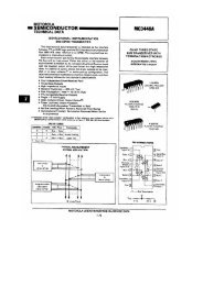
MJE15034 NPN, MJE15035 PNP Complementary ... - ClassicCmp...
MJE15034 NPN, MJE15035 PNP Complementary ... - ClassicCmp...
MJE15034 NPN, MJE15035 PNP Complementary ... - ClassicCmp...

Create successful ePaper yourself
Turn your PDF publications into a flip-book with our unique Google optimized e-Paper software.
<strong>MJE15034</strong> <strong>NPN</strong>,<br />
<strong>MJE15035</strong> <strong>PNP</strong><br />
Preferred Device<br />
<strong>Complementary</strong> Silicon<br />
Plastic Power Transistors<br />
TO−220, <strong>NPN</strong> & <strong>PNP</strong> Devices<br />
. . . designed for use as high−frequency drivers in audio amplifiers.<br />
• hFE = 100 (Min) @ IC = 0.5 Adc<br />
= 10 (Min) @ IC = 2.0 Adc<br />
• Collector−Emitter Sustaining Voltage −<br />
VCEO(sus) = 350 Vdc (Min) − <strong>MJE15034</strong>, <strong>MJE15035</strong><br />
• High Current Gain − Bandwidth Product<br />
fT = 30 MHz (Min) @ IC = 500 mAdc<br />
• TO−220AB Compact Package<br />
• Epoxy meets UL 94 V−0 @ 0.125 in<br />
• ESD Ratings: Machine Model: C<br />
Human Body Model: 3B<br />
MAXIMUM RATINGS<br />
Rating Symbol<br />
<strong>MJE15034</strong><br />
<strong>MJE15035</strong> Unit<br />
Collector−Emitter Voltage VCEO 350 Vdc<br />
Collector−Base Voltage VCB 350 Vdc<br />
Emitter−Base Voltage VEB 5.0 Vdc<br />
Collector Current − Continuous<br />
IC 4.0 Adc<br />
− Peak<br />
8.0<br />
Base Current I B 1.0 Adc<br />
Total Power Dissipation @ T C = 25�C<br />
Derate above 25�C<br />
Total Power Dissipation @ T A = 25�C<br />
Derate above 25�C<br />
Operating and Storage Junction<br />
Temperature Range<br />
THERMAL CHARACTERISTICS<br />
© Semiconductor Components Industries, LLC, 2003<br />
November, 2003 − Rev. 2<br />
P D<br />
P D<br />
T J, T stg<br />
50<br />
0.40<br />
2.0<br />
0.016<br />
– 65 to<br />
+150<br />
Watts<br />
W/�C<br />
Watts<br />
W/�C<br />
Characteristic Symbol Max Unit<br />
Thermal Resistance, Junction to Case RθJC 2.5 �C/W<br />
Thermal Resistance, Junction to Ambient RθJA 62.5 �C/W<br />
�C<br />
1 2 3<br />
4.0 AMPERES<br />
POWER TRANSISTORS<br />
COMPLEMENTARY<br />
SILICON<br />
350 VOLTS<br />
50 WATTS<br />
4<br />
http://onsemi.com<br />
TO−220AB<br />
CASE 221A<br />
STYLE 1<br />
STYLE 1:<br />
PIN 1. BASE<br />
2. COLLECTOR<br />
3. EMITTER<br />
4. COLLECTOR<br />
MARKING DIAGRAM<br />
& PIN ASSIGNMENT<br />
MJE1503x<br />
LLYWW<br />
MJE1503x = Device Code<br />
LL = Location Code<br />
Y = Year<br />
WW = Work Week<br />
ORDERING INFORMATION<br />
Device Package Shipping<br />
<strong>MJE15034</strong> TO−220AB 50 Units/Rail<br />
<strong>MJE15035</strong> TO−220AB 50 Units/Rail<br />
Preferred devices are recommended choices for future use<br />
and best overall value.<br />
1 Publication Order Number:<br />
<strong>MJE15034</strong>/D
PD, POWER DISSIPATION (WATTS)<br />
T A<br />
3.0<br />
2.0<br />
1.0<br />
0<br />
T C<br />
60<br />
40<br />
20<br />
0<br />
0<br />
20<br />
T A<br />
T C<br />
T, TEMPERATURE (°C)<br />
Figure 1. Power Derating<br />
<strong>MJE15034</strong> <strong>NPN</strong>, <strong>MJE15035</strong> <strong>PNP</strong><br />
40 60 80 100 120 140 160<br />
ELECTRICAL CHARACTERISTICS (T C = 25�C unless otherwise noted)<br />
Characteristic<br />
I C, COLLECTOR CURRENT (AMPS)<br />
10<br />
1.0<br />
0.1<br />
http://onsemi.com<br />
2<br />
DC<br />
100mS<br />
0.01<br />
1.0 10 100 1000<br />
VCE, COLLECTOR−EMITTER VOLTAGE (V)<br />
Figure 2. Active Region Safe Operating Area<br />
Symbol<br />
ÎÎÎÎÎÎÎÎÎÎÎÎÎÎÎÎÎÎÎÎÎÎÎÎÎÎÎÎÎÎÎÎÎ<br />
ÎÎÎÎÎÎÎÎÎÎÎÎÎÎÎÎÎÎÎÎÎÎ ÎÎÎÎÎ ÎÎÎ ÎÎÎÎ ÎÎÎ<br />
ÎÎÎÎÎÎÎÎÎÎÎÎÎÎÎÎÎÎÎÎÎÎÎÎÎÎÎÎÎÎÎÎÎ<br />
OFF CHARACTERISTICS<br />
Collector−Emitter Sustaining Voltage (Note 1) (I C = 10 mAdc, I B = 0)<br />
V CEO(sus)<br />
ÎÎÎÎÎ ÎÎÎ ÎÎÎÎ ÎÎÎ<br />
ÎÎÎÎÎÎÎÎÎÎÎÎÎÎÎÎÎÎÎÎÎÎÎÎÎÎÎÎÎÎÎÎÎ<br />
ÎÎÎÎÎÎÎÎÎÎÎÎÎÎÎÎÎÎÎÎÎÎ<br />
ÎÎÎÎÎÎÎÎÎÎÎÎÎÎÎÎÎÎÎÎÎÎ ÎÎÎÎÎ ÎÎÎ ÎÎÎÎ ÎÎÎ<br />
ÎÎÎÎÎÎÎÎÎÎÎÎÎÎÎÎÎÎÎÎÎÎÎÎÎÎÎÎÎÎÎÎÎ<br />
Collector Cutoff Current (V CB = 350 Vdc, I E = 0)<br />
Emitter Cutoff Current (V BE = 5.0 Vdc, I C = 0)<br />
ÎÎÎÎÎ ÎÎÎÎ<br />
ÎÎÎÎÎÎÎÎÎÎÎÎÎÎÎÎÎÎÎÎÎÎ<br />
ÎÎÎÎÎ ÎÎÎ<br />
ÎÎÎÎ ÎÎÎ<br />
ÎÎÎÎ ÎÎÎ<br />
ÎÎÎÎÎÎÎÎÎÎÎÎÎÎÎÎÎÎÎÎÎÎ ÎÎÎÎÎ ÎÎÎ ÎÎÎÎ ÎÎÎ<br />
ÎÎÎ<br />
ÎÎÎÎÎ<br />
ÎÎÎÎÎÎÎÎÎÎÎÎÎÎÎÎÎÎÎÎÎÎ<br />
ON CHARACTERISTICS (Note 1)<br />
DC Current Gain<br />
ÎÎÎÎÎ ÎÎÎ ÎÎÎÎ ÎÎÎ<br />
ÎÎÎÎÎÎÎÎÎÎÎÎÎÎÎÎÎÎÎÎÎÎÎÎÎÎÎÎÎÎÎÎÎ<br />
ÎÎÎÎÎÎÎÎÎÎÎÎÎÎÎÎÎÎÎÎÎÎ<br />
ÎÎÎÎÎÎÎÎÎÎÎÎÎÎÎÎÎÎÎÎÎÎ ÎÎÎÎÎ ÎÎÎ ÎÎÎÎ ÎÎÎ<br />
ÎÎÎÎÎÎÎÎÎÎÎÎÎÎÎÎÎÎÎÎÎÎÎÎÎÎÎÎÎÎÎÎÎ<br />
(IC = 0.1 Adc, VCE = 5.0 Vdc)<br />
(IC = 0.5 Adc, VCE = 5.0 Vdc)<br />
(IC = 1.0 Adc, VCE = 5.0 Vdc)<br />
(IC = 2.0 Adc, VCE = 5.0 Vdc)<br />
ÎÎÎÎÎÎÎÎÎÎÎÎÎÎÎÎÎÎÎÎÎÎ ÎÎÎÎÎÎÎÎÎÎ<br />
ÎÎÎÎÎ<br />
ÎÎÎÎ ÎÎÎ<br />
ÎÎÎ<br />
ÎÎÎÎÎ<br />
ÎÎÎÎÎÎÎÎÎÎÎÎÎÎÎÎÎÎÎÎÎÎ<br />
Collector−Emitter Saturation Voltage (IC = 1.0 Adc, IB = 0.1 Adc) ÎÎÎÎÎ − ÎÎÎÎ 0.5 VCE(sat) ÎÎÎ Vdc<br />
Base−Emitter On Voltage (IC = 1.0 Adc, VCE = 5.0 Vdc) ÎÎÎÎÎ − ÎÎÎÎ 1.0 VBE(on) ÎÎÎ Vdc<br />
ÎÎÎÎÎÎÎÎÎÎÎÎÎÎÎÎÎÎÎÎÎÎ ÎÎÎ ÎÎÎÎ ÎÎÎ<br />
ÎÎÎÎÎ<br />
ÎÎÎÎ ÎÎÎ<br />
ÎÎÎÎÎÎÎÎÎÎÎÎÎÎÎÎÎÎÎÎÎÎ ÎÎÎ<br />
ÎÎÎÎÎ<br />
ÎÎÎÎÎÎÎÎÎÎÎÎÎÎÎÎÎÎÎÎÎÎ<br />
DYNAMIC CHARACTERISTICS<br />
ÎÎÎÎÎ ÎÎÎÎ ÎÎÎ<br />
ÎÎÎÎÎÎÎÎÎÎÎÎÎÎÎÎÎÎÎÎÎÎ<br />
ÎÎÎ<br />
ÎÎÎ ÎÎÎÎ ÎÎÎ<br />
ÎÎÎÎÎÎÎÎÎÎÎÎÎÎÎÎÎÎÎÎÎÎÎÎÎÎÎÎÎÎÎÎÎ<br />
ÎÎÎÎÎ<br />
ÎÎÎÎÎÎÎÎÎÎÎÎÎÎÎÎÎÎÎÎÎÎ<br />
Current Gain − Bandwidth Product (Note 2)<br />
(IC = 500 mAdc, VCE = 10 Vdc, ftest = 1.0 MHz)<br />
ÎÎÎÎÎÎÎÎÎÎÎÎÎÎÎÎÎÎÎÎÎÎ ÎÎÎÎÎ ÎÎÎ<br />
ÎÎÎÎÎÎÎÎÎÎÎÎÎÎÎÎÎÎÎÎÎÎÎÎÎÎÎÎÎÎÎÎÎ<br />
ÎÎÎÎÎÎÎ<br />
ÎÎÎÎÎÎÎÎÎÎÎÎÎÎÎÎÎÎÎÎÎÎÎÎÎÎÎ<br />
ÎÎÎ<br />
ÎÎÎ<br />
1. Pulse Test: Pulse Width � 300 μs, Duty Cycle � 2.0%.<br />
2. f T = ⎪h fe⎪• f test.<br />
ÎÎÎÎÎ ÎÎÎ ÎÎÎÎ ÎÎÎ<br />
ÎÎÎÎÎÎÎÎÎÎÎÎÎÎÎÎÎÎÎÎÎÎ<br />
r(t), TRANSIENT THERMAL<br />
RESISTANCE (NORMALIZED)<br />
1.0<br />
0.7<br />
0.5<br />
0.3<br />
0.2<br />
D = 0.5<br />
0.2<br />
t, TIME (ms)<br />
I CBO<br />
I EBO<br />
h FE<br />
f T<br />
Min<br />
350<br />
−<br />
−<br />
100<br />
100<br />
50<br />
10<br />
Max<br />
−<br />
10<br />
10<br />
−<br />
−<br />
−<br />
−<br />
Unit<br />
Vdc<br />
μAdc<br />
μAdc<br />
30 ÎÎÎÎ − MHz<br />
0.1<br />
0.1<br />
P<br />
ZθJC(t) = r(t) RθJC<br />
(pk)<br />
0.07 0.05<br />
RθJC = 2.5°C/W MAX<br />
0.05<br />
D CURVES APPLY FOR POWER<br />
0.02<br />
PULSE TRAIN SHOWN<br />
0.03<br />
t1 READ TIME AT t1 t2 0.02<br />
0.01<br />
TJ(pk) − TC = P (pk) ZθJC(t)<br />
SINGLE PULSE<br />
DUTY CYCLE, D = t1/t2 0.01<br />
0.01 0.02 0.05 0.1 0.2 0.5 1.0 2.0 5.0 10 20 50 100 200 500 1.0 k<br />
Figure 3. Thermal Response<br />
−
h FE, DC CURRENT GAIN<br />
h FE, DC CURRENT GAIN<br />
V CE, COLLECTOR−EMITTER VOLTAGE (V)<br />
1000<br />
100<br />
10<br />
1000<br />
100<br />
10<br />
10<br />
1.0<br />
0.1<br />
T J = 150°C<br />
25°C<br />
−40°C<br />
1.0<br />
0.01 0.1 1.0 10<br />
T J = 150°C<br />
25°C<br />
−40°C<br />
I C, COLLECTOR CURRENT (AMPS)<br />
Figure 4. DC Current Gain, V CE = 5.0 V<br />
<strong>NPN</strong> <strong>MJE15034</strong><br />
1.0<br />
0.01 0.1 1.0 10<br />
I C, COLLECTOR CURRENT (AMPS)<br />
Figure 6. DC Current Gain, V CE = 20 V<br />
<strong>NPN</strong> <strong>MJE15034</strong><br />
T J = 150°C<br />
0.01<br />
0.01 0.1 1.0 10<br />
I C, COLLECTOR CURRENT (AMPS)<br />
<strong>MJE15034</strong> <strong>NPN</strong>, <strong>MJE15035</strong> <strong>PNP</strong><br />
25°C<br />
−40°C<br />
h FE, DC CURRENT GAIN<br />
h FE, DC CURRENT GAIN<br />
1000<br />
1000<br />
V CE, COLLECTOR−EMITTER VOLTAGE (V)<br />
100<br />
10<br />
100<br />
10<br />
10<br />
1.0<br />
0.1<br />
http://onsemi.com<br />
3<br />
T J = 150°C<br />
25°C<br />
−40°C<br />
1.0<br />
0.01 0.1 1.0 10<br />
T J = 150°C<br />
25°C<br />
−40°C<br />
I C/I B = 10 I C/I B = 10<br />
Figure 8. V CE(sat)<br />
<strong>NPN</strong> <strong>MJE15034</strong><br />
I C, COLLECTOR CURRENT (AMPS)<br />
Figure 5. DC Current Gain, V CE = 5.0 V<br />
<strong>PNP</strong> <strong>MJE15035</strong><br />
1.0<br />
0.01 0.1 1.0 10<br />
I C, COLLECTOR CURRENT (AMPS)<br />
Figure 7. DC Current Gain, V CE = 20 V<br />
<strong>PNP</strong> <strong>MJE15035</strong><br />
T J = 150°C<br />
−40°C<br />
25°C<br />
0.01<br />
0.01 0.1 1.0 10<br />
I C, COLLECTOR CURRENT (AMPS)<br />
Figure 9. V CE(sat)<br />
<strong>PNP</strong> <strong>MJE15035</strong>
BASE−EMITTER VOLTAGE (V)<br />
V BE(on), BASE−EMITTER VOLTAGE (V)<br />
f T, CURRENT BANDWIDTH PRODUCT (MHz)<br />
10<br />
1.0<br />
0.1<br />
0.01 0.1 1.0 10<br />
1.2<br />
1.0<br />
0.8<br />
0.6<br />
0.4<br />
0.2<br />
I C/I B = 10<br />
25°C<br />
−40°C<br />
T J = 150°C<br />
I C, COLLECTOR CURRENT (AMPS)<br />
Figure 10. V BE(sat)<br />
<strong>NPN</strong> <strong>MJE15034</strong><br />
0.0<br />
0.01 0.1 1.0 10<br />
80<br />
70<br />
60<br />
50<br />
40<br />
30<br />
20<br />
10<br />
−40°C<br />
T J = 25°C<br />
f test = 1 MHz<br />
25°C<br />
T J = 150°C<br />
I C, COLLECTOR CURRENT (AMPS)<br />
Figure 12. V BE(on)<br />
<strong>NPN</strong> <strong>MJE15034</strong><br />
V CE= 10 V<br />
0<br />
0.001 0.01 0.1 1.0 10<br />
I C, COLLECTOR CURRENT (AMPS)<br />
Figure 14. Typical Current Gain Bandwidth Product<br />
<strong>NPN</strong> <strong>MJE15034</strong><br />
<strong>MJE15034</strong> <strong>NPN</strong>, <strong>MJE15035</strong> <strong>PNP</strong><br />
BASE−EMITTER VOLTAGE (V)<br />
V BE(on), BASE−EMITTER VOLTAGE (V)<br />
f T, CURRENT BANDWIDTH PRODUCT (MHz)<br />
10<br />
1.0<br />
1.4<br />
1.2<br />
1.0<br />
0.8<br />
0.6<br />
0.4<br />
0.2<br />
http://onsemi.com<br />
4<br />
I C/I B = 10<br />
25°C<br />
−40°C<br />
T J = 150°C<br />
0.1<br />
0.01 0.1 1.0 10<br />
I C, COLLECTOR CURRENT (AMPS)<br />
Figure 11. V BE(sat)<br />
<strong>PNP</strong> <strong>MJE15035</strong><br />
−40°C<br />
25°C<br />
T J = 150°C<br />
0.0<br />
0.01 0.1 1.0 10<br />
100<br />
80<br />
60<br />
40<br />
20<br />
T J = 25°C<br />
f test = 1 MHz<br />
I C, COLLECTOR CURRENT (AMPS)<br />
Figure 13. V BE(on)<br />
<strong>PNP</strong> <strong>MJE15035</strong><br />
V CE= 10 V<br />
0<br />
0.001 0.01 0.1 1.0 10<br />
I C, COLLECTOR CURRENT (AMPS)<br />
Figure 15. Typical Current Gain Bandwidth Product<br />
<strong>PNP</strong> <strong>MJE15035</strong>
H<br />
Q<br />
Z<br />
L<br />
V<br />
G<br />
4<br />
B<br />
1 2 3<br />
N<br />
D<br />
A<br />
K<br />
F<br />
<strong>MJE15034</strong> <strong>NPN</strong>, <strong>MJE15035</strong> <strong>PNP</strong><br />
T<br />
U<br />
PACKAGE DIMENSIONS<br />
TO−220 THREE−LEAD<br />
TO−220AB<br />
CASE 221A−09<br />
ISSUE AA<br />
S<br />
R<br />
J<br />
C<br />
−T−<br />
SEATING<br />
PLANE<br />
STYLE 1:<br />
PIN 1. BASE<br />
2. COLLECTOR<br />
3. EMITTER<br />
4. COLLECTOR<br />
http://onsemi.com<br />
5<br />
NOTES:<br />
1. DIMENSIONING AND TOLERANCING PER<br />
ANSI Y14.5M, 1982.<br />
2. CONTROLLING DIMENSION: INCH.<br />
3. DIMENSION Z DEFINES A ZONE WHERE<br />
ALL BODY AND LEAD IRREGULARITIES<br />
ARE ALLOWED.<br />
INCHES MILLIMETERS<br />
DIM MIN MAX MIN MAX<br />
A 0.570 0.620 14.48 15.75<br />
B 0.380 0.405 9.66 10.28<br />
C 0.160 0.190 4.07 4.82<br />
D 0.025 0.035 0.64 0.88<br />
F 0.142 0.147 3.61 3.73<br />
G 0.095 0.105 2.42 2.66<br />
H 0.110 0.155 2.80 3.93<br />
J 0.018 0.025 0.46 0.64<br />
K 0.500 0.562 12.70 14.27<br />
L 0.045 0.060 1.15 1.52<br />
N 0.190 0.210 4.83 5.33<br />
Q 0.100 0.120 2.54 3.04<br />
R 0.080 0.110 2.04 2.79<br />
S 0.045 0.055 1.15 1.39<br />
T 0.235 0.255 5.97 6.47<br />
U 0.000 0.050 0.00 1.27<br />
V 0.045 −−− 1.15 −−−<br />
Z −−− 0.080 −−− 2.04
<strong>MJE15034</strong> <strong>NPN</strong>, <strong>MJE15035</strong> <strong>PNP</strong><br />
ON Semiconductor and are registered trademarks of Semiconductor Components Industries, LLC (SCILLC). SCILLC reserves the right to make changes without further notice<br />
to any products herein. SCILLC makes no warranty, representation or guarantee regarding the suitability of its products for any particular purpose, nor does SCILLC assume any liability<br />
arising out of the application or use of any product or circuit, and specifically disclaims any and all liability, including without limitation special, consequential or incidental damages.<br />
“Typical” parameters which may be provided in SCILLC data sheets and/or specifications can and do vary in different applications and actual performance may vary over time. All<br />
operating parameters, including “Typicals” must be validated for each customer application by customer’s technical experts. SCILLC does not convey any license under its patent rights<br />
nor the rights of others. SCILLC products are not designed, intended, or authorized for use as components in systems intended for surgical implant into the body, or other applications<br />
intended to support or sustain life, or for any other application in which the failure of the SCILLC product could create a situation where personal injury or death may occur. Should<br />
Buyer purchase or use SCILLC products for any such unintended or unauthorized application, Buyer shall indemnify and hold SCILLC and its officers, employees, subsidiaries, affiliates,<br />
and distributors harmless against all claims, costs, damages, and expenses, and reasonable attorney fees arising out of, directly or indirectly, any claim of personal injury or death<br />
associated with such unintended or unauthorized use, even if such claim alleges that SCILLC was negligent regarding the design or manufacture of the part. SCILLC is an Equal<br />
Opportunity/Affirmative Action Employer. This literature is subject to all applicable copyright laws and is not for resale in any manner.<br />
PUBLICATION ORDERING INFORMATION<br />
LITERATURE FULFILLMENT:<br />
Literature Distribution Center for ON Semiconductor<br />
P.O. Box 5163, Denver, Colorado 80217 USA<br />
Phone: 303−675−2175 or 800−344−3860 Toll Free USA/Canada<br />
Fax: 303−675−2176 or 800−344−3867 Toll Free USA/Canada<br />
Email: orderlit@onsemi.com<br />
N. American Technical Support: 800−282−9855 Toll Free<br />
USA/Canada<br />
Japan: ON Semiconductor, Japan Customer Focus Center<br />
2−9−1 Kamimeguro, Meguro−ku, Tokyo, Japan 153−0051<br />
Phone: 81−3−5773−3850<br />
http://onsemi.com<br />
6<br />
ON Semiconductor Website: http://onsemi.com<br />
Order Literature: http://www.onsemi.com/litorder<br />
For additional information, please contact your<br />
local Sales Representative.<br />
<strong>MJE15034</strong>/D