ATF-34143 DS - von Gunthard Kraus
ATF-34143 DS - von Gunthard Kraus
ATF-34143 DS - von Gunthard Kraus

Create successful ePaper yourself
Turn your PDF publications into a flip-book with our unique Google optimized e-Paper software.
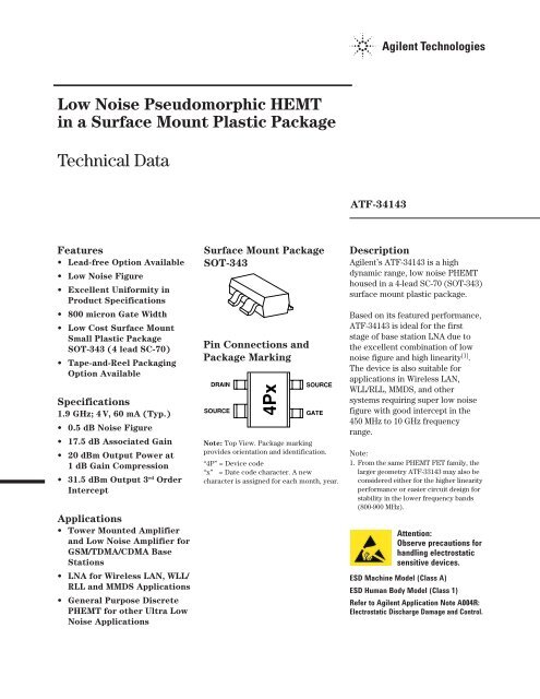
Low Noise Pseudomorphic HEMT<br />
in a Surface Mount Plastic Package<br />
Technical Data<br />
<strong>ATF</strong>-<strong>34143</strong><br />
Features<br />
• Lead-free Option Available<br />
• Low Noise Figure<br />
• Excellent Uniformity in<br />
Product Specifications<br />
• 800 micron Gate Width<br />
• Low Cost Surface Mount<br />
Small Plastic Package<br />
SOT-343 (4 lead SC-70)<br />
• Tape-and-Reel Packaging<br />
Option Available<br />
Specifications<br />
1.9 GHz; 4 V, 60 mA (Typ.)<br />
• 0.5 dB Noise Figure<br />
• 17.5 dB Associated Gain<br />
• 20 dBm Output Power at<br />
1 dB Gain Compression<br />
• 31.5 dBm Output 3 rd Order<br />
Intercept<br />
Applications<br />
• Tower Mounted Amplifier<br />
and Low Noise Amplifier for<br />
GSM/TDMA/CDMA Base<br />
Stations<br />
• LNA for Wireless LAN, WLL/<br />
RLL and MM<strong>DS</strong> Applications<br />
• General Purpose Discrete<br />
PHEMT for other Ultra Low<br />
Noise Applications<br />
Surface Mount Package<br />
SOT-343<br />
Pin Connections and<br />
Package Marking<br />
DRAIN<br />
SOURCE<br />
4Px<br />
SOURCE<br />
GATE<br />
Note: Top View. Package marking<br />
provides orientation and identification.<br />
“4P” = Device code<br />
“x” = Date code character. A new<br />
character is assigned for each month, year.<br />
Description<br />
Agilent’s <strong>ATF</strong>-<strong>34143</strong> is a high<br />
dynamic range, low noise PHEMT<br />
housed in a 4-lead SC-70 (SOT-343)<br />
surface mount plastic package.<br />
Based on its featured performance,<br />
<strong>ATF</strong>-<strong>34143</strong> is ideal for the first<br />
stage of base station LNA due to<br />
the excellent combination of low<br />
noise figure and high linearity [1] .<br />
The device is also suitable for<br />
applications in Wireless LAN,<br />
WLL/RLL, MM<strong>DS</strong>, and other<br />
systems requiring super low noise<br />
figure with good intercept in the<br />
450 MHz to 10 GHz frequency<br />
range.<br />
Note:<br />
1. From the same PHEMT FET family, the<br />
larger geometry <strong>ATF</strong>-33143 may also be<br />
considered either for the higher linearity<br />
performance or easier circuit design for<br />
stability in the lower frequency bands<br />
(800-900 MHz).<br />
Attention:<br />
Observe precautions for<br />
handling electrostatic<br />
sensitive devices.<br />
ESD Machine Model (Class A)<br />
ESD Human Body Model (Class 1)<br />
Refer to Agilent Application Note A004R:<br />
Electrostatic Discharge Damage and Control.
2<br />
<strong>ATF</strong>-<strong>34143</strong> Absolute Maximum Ratings [1]<br />
Absolute<br />
Symbol Parameter Units Maximum<br />
V <strong>DS</strong> Drain - Source Voltage [2] V 5.5<br />
V GS Gate - Source Voltage [2] V -5<br />
V GD Gate Drain Voltage [2] V -5<br />
I D Drain Current [2] mA I [3] dss<br />
P diss Total Power Dissipation [4] mW 725<br />
P in max RF Input Power dBm 17<br />
T CH Channel Temperature °C 160<br />
T STG Storage Temperature °C -65 to 160<br />
θ jc Thermal Resistance [5] °C/W 165<br />
Notes:<br />
1. Operation of this device above any one<br />
of these parameters may cause<br />
permanent damage.<br />
2. Assumes DC quiescent conditions.<br />
3. V GS = 0 volts.<br />
4. Source lead temperature is 25°C.<br />
Derate 6 mW/°C for T L > 40°C.<br />
5. Thermal resistance measured using<br />
150°C Liquid Crystal Measurement<br />
method.<br />
6. Under large signal conditions, V GS may<br />
swing positive and the drain current<br />
may exceed I dss . These conditions are<br />
acceptable as long as the maximum<br />
P diss and P in max ratings are not<br />
exceeded.<br />
I <strong>DS</strong> (mA)<br />
250<br />
200<br />
150<br />
100<br />
50<br />
+0.6 V<br />
0 V<br />
–0.6 V<br />
Product Consistency Distribution Charts [7]<br />
120<br />
100<br />
80<br />
60<br />
40<br />
20<br />
-3 Std +3 Std<br />
Cpk = 1.37245<br />
Std = 0.66<br />
9 Wafers<br />
Sample Size = 450<br />
0<br />
0 2 4 6 8<br />
V <strong>DS</strong> (V)<br />
Figure 1. Typical/Pulsed I-V Curves [6] .<br />
(V GS = -0.2 V per step)<br />
0<br />
29 30 31 32 33 34 35<br />
OIP3 (dBm)<br />
Figure 2. OIP3 @ 2 GHz, 4 V, 60 mA.<br />
LSL=29.0, Nominal=31.8, USL=35.0<br />
120<br />
100<br />
80<br />
Cpk = 2.69167<br />
Std = 0.04<br />
9 Wafers<br />
Sample Size = 450<br />
120<br />
100<br />
80<br />
Cpk = 2.99973<br />
Std = 0.15<br />
9 Wafers<br />
Sample Size = 450<br />
60<br />
-3 Std +3 Std<br />
60<br />
-3 Std +3 Std<br />
40<br />
40<br />
20<br />
20<br />
0<br />
0 0.2 0.4 0.6 0.8<br />
NF (dB)<br />
Figure 3. NF @ 2 GHz, 4 V, 60 mA.<br />
LSL=0.1, Nominal=0.47, USL=0.8<br />
0<br />
16 16.5 17 17.5 18 18.5 19<br />
GAIN (dB)<br />
Figure 4. Gain @ 2 GHz, 4 V, 60 mA.<br />
LSL=16.0, Nominal=17.5, USL=19.0<br />
Notes:<br />
7. Distribution data sample size is 450<br />
samples taken from 9 different wafers.<br />
Future wafers allocated to this product<br />
may have nominal values anywhere<br />
within the upper and lower spec limits.<br />
8. Measurements made on production<br />
test board. This circuit represents a<br />
trade-off between an optimal noise<br />
match and a realizeable match based<br />
on production test requirements.<br />
Circuit losses have been de-embedded<br />
from actual measurements.
3<br />
<strong>ATF</strong>-<strong>34143</strong> Electrical Specifications<br />
T A = 25°C, RF parameters measured in a test circuit for a typical device<br />
Symbol Parameters and Test Conditions Units Min. Typ. [2] Max.<br />
I dss<br />
[1] Saturated Drain Current V <strong>DS</strong> = 1.5 V, V GS = 0 V mA 90 118 145<br />
V P<br />
[1] Pinchoff Voltage V <strong>DS</strong> = 1.5 V, I <strong>DS</strong> = 10% of I dss V -0.65 -0.5 -0.35<br />
I d Quiescent Bias Current V GS = 0.34 V, V <strong>DS</strong> = 4 V mA — 60 —<br />
g m<br />
[1] Transconductance V <strong>DS</strong> = 1.5 V, g m = I dss /V P mmho 180 230 —<br />
I GDO Gate to Drain Leakage Current V GD = 5 V µA 500<br />
I gss Gate Leakage Current V GD = V GS = -4 V µA — 30 300<br />
NF Noise Figure f = 2 GHz V <strong>DS</strong> = 4 V, I <strong>DS</strong> = 60 mA dB 0.5 0.8<br />
V <strong>DS</strong> = 4 V, I <strong>DS</strong> = 30 mA 0.5<br />
f = 900 MHz V <strong>DS</strong> = 4 V, I <strong>DS</strong> = 60 mA dB 0.4<br />
G a Associated Gain f = 2 GHz V <strong>DS</strong> = 4 V, I <strong>DS</strong> = 60 mA dB 16 17.5 19<br />
V <strong>DS</strong> = 4 V, I <strong>DS</strong> = 30 mA 17<br />
f = 900 MHz V <strong>DS</strong> = 4 V, I <strong>DS</strong> = 60 mA dB 21.5<br />
OIP3 Output 3 rd Order f = 2 GHz V <strong>DS</strong> = 4 V, I <strong>DS</strong> = 60 mA dBm 29 31.5<br />
Intercept Point [3] +5 dBm P out /Tone V <strong>DS</strong> = 4 V, I <strong>DS</strong> = 30 mA 30<br />
f = 900 MHz V <strong>DS</strong> = 4 V, I <strong>DS</strong> = 60 mA dBm 31<br />
+5 dBm P out /Tone<br />
P 1dB 1 dB Compressed f = 2 GHz V <strong>DS</strong> = 4 V, I <strong>DS</strong> = 60 mA dBm 20<br />
Intercept Point [3] V <strong>DS</strong> = 4 V, I <strong>DS</strong> = 30 mA 19<br />
f = 900 MHz V <strong>DS</strong> = 4 V, I <strong>DS</strong> = 60 mA dBm 18.5<br />
Notes:<br />
1. Guaranteed at wafer probe level<br />
2. Typical value determined from a sample size of 450 parts from 9 wafers.<br />
3. Using production test board.<br />
Input<br />
50 Ohm<br />
Transmission<br />
Line Including<br />
Gate Bias T<br />
(0.5 dB loss)<br />
Input<br />
Matching Circuit<br />
Γ_mag = 0.30<br />
Γ_ang = 56°<br />
(0.4 dB loss)<br />
DUT<br />
50 Ohm<br />
Transmission<br />
Line Including<br />
Drain Bias T<br />
(0.5 dB loss)<br />
Output<br />
Figure 5. Block diagram of 2 GHz production test board used for Noise Figure, Associated Gain, P1dB, and OIP3 measurements.<br />
This circuit represents a trade-off between an optimal noise match and associated impedance matching circuit<br />
losses. Circuit losses have been de-embedded from actual measurements.
4<br />
<strong>ATF</strong>-<strong>34143</strong> Typical Performance Curves<br />
OIP3, P 1dB (dBm)<br />
35<br />
30<br />
25<br />
20<br />
15<br />
10<br />
OIP3<br />
P 1dB<br />
5<br />
3 V<br />
4 V<br />
0<br />
0 20 40 60 80 100 120 140<br />
I <strong>DS</strong>Q (mA)<br />
Figure 6. OIP3 and P 1dB vs. I <strong>DS</strong> and<br />
V <strong>DS</strong> Tuned for NF @ 4 V, 60 mA at<br />
2 GHz. [1,2]<br />
ASSOCIATED GAIN (dB)<br />
20<br />
15<br />
10<br />
5<br />
3 V<br />
4 V<br />
0<br />
0 20 40 60 80 100 120<br />
CURRENT (mA)<br />
Figure 7. Associated Gain vs. Current<br />
(I d ) and Voltage (V D ) at 2 GHz.[1,2]<br />
NOISE FIGURE (dB)<br />
1<br />
0.8<br />
0.6<br />
0.4<br />
0.2<br />
0<br />
0 20 40 60 80 100 120<br />
CURRENT (mA)<br />
3 V<br />
4 V<br />
Figure 8. Noise Figure vs. Current<br />
(I d ) and Voltage (V <strong>DS</strong> ) at 2 GHz. [1,2]<br />
OIP3, P 1dB (dBm)<br />
35<br />
30<br />
25<br />
20<br />
15<br />
10<br />
5<br />
0<br />
OIP3<br />
P 1dB<br />
0 20 40 60 80 100 120<br />
I <strong>DS</strong>Q (mA)<br />
3 V<br />
4 V<br />
Figure 9. OIP3 and P 1dB vs. I <strong>DS</strong> and<br />
V <strong>DS</strong> Tuned for NF @ 4 V, 60 mA at<br />
900 MHz. [1,2]<br />
ASSOCIATED GAIN (dB)<br />
25<br />
20<br />
15<br />
10<br />
5<br />
0<br />
CURRENT (mA)<br />
3 V<br />
4 V<br />
0 20 40 60 80 100 120<br />
Figure 10. Associated Gain vs. Current<br />
(I d ) and Voltage (V D ) at 900 MHz. [1,2]<br />
NOISE FIGURE (dB)<br />
0.7<br />
0.6<br />
0.5<br />
0.4<br />
0.3<br />
0.2<br />
0.1<br />
3 V<br />
4 V<br />
0<br />
0 20 40 60 80 100 120<br />
CURRENT (mA)<br />
Figure 11. Noise Figure vs. Current<br />
(I d ) and Voltage (V <strong>DS</strong> ) at 900 MHz. [1,2]<br />
1.2<br />
25<br />
Fmin (dB)<br />
1.0<br />
0.8<br />
0.6<br />
0.4<br />
0.2<br />
0<br />
0 2.0 4.0 6.0<br />
FREQUENCY (GHz)<br />
60 mA<br />
40 mA<br />
20 mA<br />
Figure 12. Fmin vs. Frequency and<br />
Current at 4 V.<br />
Ga (dB)<br />
20<br />
15<br />
10<br />
5<br />
0 1.0 2.0 3.0 4.0 5.0 6.0<br />
FREQUENCY (GHz)<br />
Figure 13. Associated Gain vs.<br />
Frequency and Current at 4 V.<br />
Notes:<br />
1. Measurements made on a fixed toned production test board that was tuned for optimal gain match with reasonable noise figure at 4 V,<br />
60 mA bias. This circuit represents a trade-off between optimal noise match, maximum gain match, and a realizable match based on<br />
production test board requirements. Circuit losses have been de-embedded from actual measurements.<br />
2. P 1dB measurements are performed with passive biasing. Quicescent drain current, I <strong>DS</strong>Q , is set with zero RF drive applied. As P 1dB is<br />
approached, the drain current may increase or decrease depending on frequency and dc bias point. At lower values of I <strong>DS</strong>Q the device<br />
is running closer to class B as power output approaches P 1dB . This results in higher PAE (power added efficiency) when compared to<br />
a device that is driven by a constant current source as is typically done with active biasing. As an example, at a V <strong>DS</strong> = 4 V and<br />
I <strong>DS</strong>Q = 10 mA, I d increases to 62 mA as a P 1dB of +19 dBm is approached.<br />
60 mA<br />
40 mA<br />
20 mA
5<br />
<strong>ATF</strong>-<strong>34143</strong> Typical Performance Curves, continued<br />
Ga (dB)<br />
25<br />
20<br />
15<br />
85 °C<br />
25 °C<br />
-40 °C<br />
1.5<br />
1.0<br />
0.5<br />
NF (dB)<br />
10<br />
0<br />
0 2000 4000 6000 8000<br />
FREQUENCY (GHz)<br />
Figure 14. Fmin and G a vs. Frequency<br />
and Temperature at V <strong>DS</strong> = 4 V, I <strong>DS</strong> = 60 mA.<br />
P1dB, OIP3 (dBm)<br />
33<br />
31<br />
29<br />
27<br />
25<br />
23<br />
21<br />
19<br />
OIP3<br />
P 1dB<br />
85 °C<br />
25 °C<br />
-40 °C<br />
17<br />
0 2000 4000 6000 8000<br />
FREQUENCY (MHz)<br />
Figure 15. P 1dB , IP3 vs. Frequency and<br />
Temperature at V <strong>DS</strong> = 4 V, I <strong>DS</strong> = 60 mA. [1]<br />
GAIN (dB), OP1dB, and OIP3 (dBm)<br />
35<br />
30<br />
25<br />
20<br />
15<br />
10<br />
5<br />
0<br />
0 20 40 60 80 100 120 140<br />
I <strong>DS</strong>Q (mA)<br />
Gain<br />
OP1dB<br />
OIP3<br />
NF<br />
5.0<br />
4.5<br />
4.0<br />
3.5<br />
3.0<br />
2.5<br />
2.0<br />
1.5<br />
1.0<br />
0.5<br />
0<br />
Figure 16. NF, Gain, OP1dB and OIP3<br />
vs. I <strong>DS</strong> at 4 V and 3.9 GHz Tuned for<br />
Noise Figure. [1]<br />
NOISE FIGURE (dB)<br />
30<br />
5.0<br />
27<br />
4.5<br />
24<br />
4.0<br />
21<br />
3.5<br />
18<br />
Gain<br />
OP1dB<br />
3.0<br />
15<br />
OIP3<br />
NF<br />
2.5<br />
12<br />
2.0<br />
9<br />
1.5<br />
6<br />
1.0<br />
3<br />
0.5<br />
0<br />
0<br />
0 20 40 60 80 100 120<br />
I <strong>DS</strong>Q (mA)<br />
Figure 17. NF, Gain, OP1dB and OIP3<br />
vs. I <strong>DS</strong> at 4 V and 5.8 GHz Tuned for<br />
Noise Figure. [1]<br />
GAIN (dB), OP1dB, and OIP3 (dBm)<br />
NOISE FIGURE (dB)<br />
P 1dB (dBm)<br />
25<br />
20<br />
15<br />
10<br />
5<br />
0<br />
-5<br />
0 50 100 150<br />
I <strong>DS</strong> (mA)<br />
3 V<br />
4 V<br />
Figure 18. P 1dB vs. I <strong>DS</strong> Active Bias<br />
Tuned for NF @ 4V, 60 mA at 2 GHz.<br />
P 1dB (dBm)<br />
25<br />
20<br />
15<br />
10<br />
5<br />
0<br />
3 V<br />
4 V<br />
-5<br />
0 50 100 150<br />
I <strong>DS</strong> (mA)<br />
Figure 19. P 1dB vs. I <strong>DS</strong> Active Bias<br />
Tuned for min NF @ 4V, 60 mA at<br />
900 MHz.<br />
Note:<br />
1. P 1dB measurements are performed with passive biasing. Quicescent drain current, I <strong>DS</strong>Q , is set with zero RF drive applied. As P 1dB is<br />
approached, the drain current may increase or decrease depending on frequency and dc bias point. At lower values of I <strong>DS</strong>Q the device<br />
is running closer to class B as power output approaches P 1dB . This results in higher PAE (power added efficiency) when compared to<br />
a device that is driven by a constant current source as is typically done with active biasing. As an example, at a V <strong>DS</strong> = 4 V and<br />
I <strong>DS</strong>Q = 10 mA, I d increases to 62 mA as a P 1dB of +19 dBm is approached.
6<br />
<strong>ATF</strong>-<strong>34143</strong> Power Parameters tuned for Power, V <strong>DS</strong> = 4 V, I <strong>DS</strong>Q = 120 mA<br />
Gamma Gamma<br />
Freq P 1dB I d G 1dB PAE 1dB P 3dBm I d PAE 3dB Out_mag Out_ang<br />
(GHz) (dBm) (mA) (dB) (%) (dBm) (mA) (%) (Mag) (Degrees)<br />
0.9 20.9 114 25.7 27 22.8 108 44 0.34 136<br />
1.5 21.7 115 21.9 32 23.1 95 53 0.31 152<br />
1.8 21.3 111 20.5 30 23.0 105 47 0.30 164<br />
2 22.0 106 19.5 37 23.7 115 50 0.28 171<br />
4 22.7 110 12.7 40 23.6 111 47 0.26 -135<br />
6 23.3 115 9.2 41 24.2 121 44 0.24 -66<br />
<strong>ATF</strong>-<strong>34143</strong> Power Parameters tuned for Power, V <strong>DS</strong> = 4 V, I <strong>DS</strong>Q = 60 mA<br />
Gamma Gamma<br />
Freq P 1dB I d G 1dB PAE 1dB P 3dBm I d PAE 3dB Out_mag Out_ang<br />
(GHz) (dBm) (mA) (dB) (%) (dBm) (mA) (%) (Mag) (Degrees)<br />
0.9 18.2 75 27.5 22 20.5 78 36 0.48 102<br />
1.5 18.7 58 24.5 32 20.8 59 51 0.45 117<br />
1.8 18.8 57 23.0 33 21.1 71 45 0.42 126<br />
2 18.8 59 22.2 32 21.9 81 47 0.40 131<br />
4 20.2 66 13.9 38 22.0 77 48 0.25 -162<br />
6 21.2 79 9.9 37 23.5 102 46 0.18 -77<br />
P out (dBm), G (dB),<br />
PAE (%)<br />
80<br />
50<br />
40<br />
30<br />
20<br />
10<br />
P out<br />
0<br />
Gain<br />
PAE<br />
-10<br />
-30 -20 -10 0 10 20<br />
P in (dBm)<br />
Figure 20. Swept Power Tuned for<br />
Power at 2 GHz, V <strong>DS</strong> = 4 V, I <strong>DS</strong>Q = 120 mA.<br />
P out (dBm), G (dB),<br />
PAE (%)<br />
80<br />
60<br />
40<br />
20<br />
0<br />
P out<br />
Gain<br />
PAE<br />
-20<br />
-30 -20 -10 0 10 20<br />
P in (dBm)<br />
Figure 21. Swept Power Tuned for<br />
Power at 2 GHz, V <strong>DS</strong> = 4 V, I <strong>DS</strong>Q = 60 mA.<br />
Notes:<br />
1. P 1dB measurements are performed with passive biasing. Quicescent drain current, I <strong>DS</strong>Q , is set with zero RF drive applied. As P 1dB is<br />
approached, the drain current may increase or decrease depending on frequency and dc bias point. At lower values of I <strong>DS</strong>Q the device<br />
is running closer to class B as power output approaches P 1dB . This results in higher PAE (power added efficiency) when compared to<br />
a device that is driven by a constant current source as is typically done with active biasing. As an example, at a V <strong>DS</strong> = 4 V and<br />
I <strong>DS</strong>Q = 10 mA, I d increases to 62 mA as a P 1dB of +19 dBm is approached.<br />
2. PAE(%) = ((Pout – Pin)/Pdc) x 100<br />
3. Gamma out is the reflection coefficient of the matching circuit presented to the output of the device.
7<br />
<strong>ATF</strong>-<strong>34143</strong> Typical Scattering Parameters, V <strong>DS</strong> = 3 V, I <strong>DS</strong> = 20 mA<br />
Freq. S 11 S 21 S 12 S 22 MSG/MAG<br />
GHz Mag. Ang. dB Mag. Ang. dB Mag. Ang. Mag. Ang. dB<br />
0.5 0.96 -37 20.07 10.079 153 -29.12 0.035 68 0.40 -35 24.59<br />
0.8 0.91 -60 19.68 9.642 137 -26.02 0.050 56 0.34 -56 22.85<br />
1.0 0.87 -76 18.96 8.867 126 -24.29 0.061 48 0.32 -71 21.62<br />
1.5 0.81 -104 17.43 7.443 106 -22.27 0.077 34 0.29 -98 19.85<br />
1.8 0.78 -115 16.70 6.843 98 -21.62 0.083 28 0.28 -110 19.16<br />
2.0 0.75 -126 16.00 6.306 90 -21.11 0.088 23 0.26 -120 18.55<br />
2.5 0.72 -145 14.71 5.438 75 -20.45 0.095 15 0.25 -140 17.58<br />
3.0 0.69 -162 13.56 4.762 62 -19.83 0.102 7 0.23 -156 16.69<br />
4.0 0.65 166 11.61 3.806 38 -19.09 0.111 -8 0.22 174 15.35<br />
5.0 0.64 139 10.01 3.165 16 -18.49 0.119 -21 0.22 146 14.25<br />
6.0 0.65 114 8.65 2.706 -5 -18.06 0.125 -35 0.23 118 13.35<br />
7.0 0.66 89 7.33 2.326 -27 -17.79 0.129 -49 0.25 91 10.91<br />
8.0 0.69 67 6.09 2.017 -47 -17.52 0.133 -62 0.29 67 9.71<br />
9.0 0.72 48 4.90 1.758 -66 -17.39 0.135 -75 0.34 46 8.79<br />
10.0 0.75 30 3.91 1.568 -86 -17.08 0.140 -88 0.39 28 8.31<br />
11.0 0.77 10 2.88 1.393 -105 -16.95 0.142 -103 0.43 10 7.56<br />
12.0 0.80 -10 1.74 1.222 -126 -16.95 0.142 -118 0.47 -10 6.83<br />
13.0 0.83 -29 0.38 1.045 -145 -17.39 0.135 -133 0.53 -28 6.18<br />
14.0 0.85 -44 -0.96 0.895 -161 -17.86 0.128 -145 0.58 -42 5.62<br />
15.0 0.86 -55 -2.06 0.789 -177 -18.13 0.124 -156 0.62 -57 5.04<br />
16.0 0.85 -72 -3.09 0.701 166 -18.13 0.124 -168 0.65 -70 3.86<br />
17.0 0.85 -88 -4.22 0.615 149 -18.06 0.125 177 0.68 -85 3.00<br />
18.0 0.88 -101 -5.71 0.518 133 -18.94 0.113 165 0.71 -103 2.52<br />
<strong>ATF</strong>-<strong>34143</strong> Typical Noise Parameters<br />
V <strong>DS</strong> = 3 V, I <strong>DS</strong> = 20 mA<br />
Freq. F min Γ opt R n/50 G a<br />
GHz dB Mag. Ang. - dB<br />
0.5 0.10 0.90 13 0.16 21.8<br />
0.9 0.11 0.85 27 0.14 18.3<br />
1.0 0.11 0.84 31 0.13 17.8<br />
1.5 0.14 0.77 48 0.11 16.4<br />
1.8 0.17 0.74 57 0.10 16.0<br />
2.0 0.19 0.71 66 0.09 15.6<br />
2.5 0.23 0.65 83 0.07 14.8<br />
3.0 0.29 0.59 102 0.06 14.0<br />
4.0 0.42 0.51 138 0.03 12.6<br />
5.0 0.54 0.45 174 0.03 11.4<br />
6.0 0.67 0.42 -151 0.05 10.3<br />
7.0 0.79 0.42 -118 0.10 9.4<br />
8.0 0.92 0.45 -88 0.18 8.6<br />
9.0 1.04 0.51 -63 0.30 8.0<br />
10.0 1.16 0.61 -43 0.46 7.5<br />
MSG/MAG and<br />
S 21 (dB)<br />
25<br />
20<br />
15<br />
10<br />
5<br />
0<br />
-5<br />
MSG<br />
S 21<br />
MAG<br />
-10<br />
0 2 4 6 8 10 12 14 16 18<br />
FREQUENCY (GHz)<br />
Figure 23. MSG/MAG and |S 21 | 2 vs.<br />
Frequency at 3 V, 20 mA.<br />
Notes:<br />
1. Fmin values at 2 GHz and higher are based on measurements while the Fmins below 2 GHz have been extrapolated. The Fmin values<br />
are based on a set of 16 noise figure measurements made at 16 different impedances using an ATN NP5 test system. From these<br />
measurements a true Fmin is calculated. Refer to the noise parameter application section for more information.<br />
2. S and noise parameters are measured on a microstrip line made on 0.025 inch thick alumina carrier. The input reference plane is at the<br />
end of the gate lead. The output reference plane is at the end of the drain lead. The parameters include the effect of four plated<br />
through via holes connecting source landing pads on top of the test carrier to the microstrip ground plane on the bottom side of the<br />
carrier. Two 0.020 inch diameter via holes are placed within 0.010 inch from each source lead contact point, one via on each side of<br />
that point.
8<br />
<strong>ATF</strong>-<strong>34143</strong> Typical Scattering Parameters, V <strong>DS</strong> = 3 V, I <strong>DS</strong> = 40 mA<br />
Freq. S 11 S 21 S 12 S 22 MSG/MAG<br />
GHz Mag. Ang. dB Mag. Ang. dB Mag. Ang. Mag. Ang. dB<br />
0.5 0.96 -40 21.32 11.645 151 -30.46 0.030 68 0.29 -43 25.89<br />
0.8 0.89 -64 20.79 10.950 135 -27.33 0.043 56 0.24 -70 24.06<br />
1.0 0.85 -81 19.96 9.956 124 -25.68 0.052 49 0.24 -88 22.82<br />
1.5 0.79 -109 18.29 8.209 104 -23.61 0.066 36 0.23 -118 20.95<br />
1.8 0.76 -121 17.50 7.495 96 -22.97 0.071 32 0.23 -130 20.24<br />
2.0 0.74 -131 16.75 6.876 88 -22.38 0.076 27 0.22 -141 19.57<br />
2.5 0.70 -150 15.39 5.880 74 -21.51 0.084 19 0.22 -160 18.45<br />
3.0 0.67 -167 14.19 5.120 61 -20.92 0.090 12 0.22 -176 17.55<br />
4.0 0.64 162 12.18 4.063 38 -19.83 0.102 -1 0.21 157 16.00<br />
5.0 0.64 135 10.54 3.365 16 -19.02 0.112 -14 0.22 131 14.78<br />
6.0 0.65 111 9.15 2.867 -5 -18.34 0.121 -28 0.24 105 12.91<br />
7.0 0.66 87 7.80 2.454 -26 -17.86 0.128 -42 0.28 81 11.03<br />
8.0 0.69 65 6.55 2.125 -46 -17.46 0.134 -55 0.32 60 9.93<br />
9.0 0.73 46 5.33 1.848 -65 -17.20 0.138 -69 0.37 40 9.07<br />
10.0 0.76 28 4.33 1.647 -84 -16.83 0.144 -84 0.41 23 8.59<br />
11.0 0.78 9 3.30 1.462 -104 -16.65 0.147 -99 0.45 5 7.84<br />
12.0 0.80 -11 2.15 1.281 -123 -16.65 0.147 -114 0.50 -14 7.15<br />
13.0 0.83 -30 0.79 1.095 -142 -17.08 0.140 -130 0.55 -31 6.50<br />
14.0 0.86 -44 -0.53 0.941 -158 -17.52 0.133 -142 0.60 -45 5.96<br />
15.0 0.87 -56 -1.61 0.831 -174 -17.72 0.130 -154 0.64 -59 5.39<br />
16.0 0.86 -72 -2.60 0.741 169 -17.72 0.130 -166 0.66 -73 4.21<br />
17.0 0.86 -88 -3.72 0.652 153 -17.79 0.129 179 0.69 -88 3.43<br />
18.0 0.88 -102 -5.15 0.553 137 -18.64 0.117 166 0.72 -105 2.95<br />
<strong>ATF</strong>-<strong>34143</strong> Typical Noise Parameters<br />
V <strong>DS</strong> = 3 V, I <strong>DS</strong> = 40 mA<br />
Freq. F min Γ opt R n/50 G a<br />
GHz dB Mag. Ang. - dB<br />
0.5 0.10 0.87 13 0.16 23.0<br />
0.9 0.13 0.82 28 0.13 19.6<br />
1.0 0.14 0.80 32 0.13 19.2<br />
1.5 0.17 0.73 50 0.1 17.7<br />
1.8 0.21 0.70 61 0.09 17.1<br />
2.0 0.23 0.66 68 0.08 16.7<br />
2.5 0.29 0.60 87 0.06 15.8<br />
3.0 0.35 0.54 106 0.05 14.9<br />
4.0 0.47 0.46 144 0.03 13.4<br />
5.0 0.6 0.41 -178 0.03 12.1<br />
6.0 0.72 0.39 -142 0.06 10.9<br />
7.0 0.85 0.41 -109 0.12 9.9<br />
8.0 0.97 0.45 -80 0.21 9.1<br />
9.0 1.09 0.52 -56 0.34 8.4<br />
10.0 1.22 0.61 -39 0.50 8.0<br />
MSG/MAG and<br />
S 21 (dB)<br />
30<br />
25<br />
20<br />
15<br />
10<br />
5<br />
0<br />
-5<br />
MSG<br />
S 21<br />
MAG<br />
-10<br />
0 2 4 6 8 10 12 14 16 18<br />
FREQUENCY (GHz)<br />
Figure 24. MSG/MAG and |S 21 | 2 vs.<br />
Frequency at 3 V, 40 mA.<br />
Notes:<br />
1. Fmin values at 2 GHz and higher are based on measurements while the Fmins below 2 GHz have been extrapolated. The Fmin values<br />
are based on a set of 16 noise figure measurements made at 16 different impedances using an ATN NP5 test system. From these<br />
measurements a true Fmin is calculated. Refer to the noise parameter application section for more information.<br />
2. S and noise parameters are measured on a microstrip line made on 0.025 inch thick alumina carrier. The input reference plane is at the<br />
end of the gate lead. The output reference plane is at the end of the drain lead. The parameters include the effect of four plated<br />
through via holes connecting source landing pads on top of the test carrier to the microstrip ground plane on the bottom side of the<br />
carrier. Two 0.020 inch diameter via holes are placed within 0.010 inch from each source lead contact point, one via on each side of<br />
that point.
9<br />
<strong>ATF</strong>-<strong>34143</strong> Typical Scattering Parameters, V <strong>DS</strong> = 4 V, I <strong>DS</strong> = 40 mA<br />
Freq. S 11 S 21 S 12 S 22 MSG/MAG<br />
GHz Mag. Ang. dB Mag. Ang. dB Mag. Ang. Mag. Ang. dB<br />
0.5 0.95 -40 21.56 11.973 151 0.03 0.030 68 0.33 -39 26.01<br />
0.8 0.89 -65 21.02 11.252 135 0.04 0.042 56 0.27 -63 24.28<br />
1.0 0.85 -82 20.19 10.217 123 0.05 0.051 48 0.26 -80 23.02<br />
1.5 0.78 -109 18.49 8.405 104 0.06 0.064 36 0.24 -109 21.18<br />
1.8 0.73 -131 16.93 7.024 87 0.07 0.074 27 0.22 -131 20.46<br />
2.0 0.70 -150 15.57 6.002 73 0.08 0.081 19 0.21 -150 19.77<br />
2.5 0.67 -167 14.36 5.223 61 0.09 0.087 12 0.20 -167 18.70<br />
3.0 0.64 162 12.34 4.141 37 0.10 0.098 -1 0.19 165 17.75<br />
4.0 0.63 135 10.70 3.428 16 0.11 0.108 -13 0.20 138 16.26<br />
5.0 0.64 111 9.32 2.923 -6 0.12 0.117 -27 0.21 111 15.02<br />
6.0 0.66 87 7.98 2.506 -26 0.12 0.124 -41 0.24 86 12.93<br />
7.0 0.69 65 6.74 2.173 -46 0.13 0.130 -54 0.29 63 11.14<br />
8.0 0.72 47 5.55 1.894 -65 0.13 0.134 -68 0.34 42 10.09<br />
9.0 0.76 28 4.55 1.689 -85 0.14 0.141 -82 0.38 26 9.24<br />
10.0 0.78 9 3.53 1.501 -104 0.15 0.145 -97 0.42 8 8.79<br />
11.0 0.80 -11 2.39 1.317 -124 0.15 0.145 -113 0.47 -11 8.09<br />
12.0 0.84 -29 1.02 1.125 -143 0.14 0.140 -128 0.53 -29 7.35<br />
13.0 0.86 -44 -0.30 0.966 -160 0.13 0.133 -141 0.58 -43 6.76<br />
14.0 0.87 -56 -1.38 0.853 -176 0.13 0.130 -152 0.62 -58 6.19<br />
15.0 0.86 -72 -2.40 0.759 167 0.13 0.131 -165 0.65 -71 5.62<br />
16.0 0.86 -88 -3.53 0.666 151 0.13 0.130 -180 0.68 -86 4.43<br />
17.0 0.89 -102 -4.99 0.563 134 0.12 0.119 168 0.71 -103 3.60<br />
18.0 0.89 -101.85 -4.99 0.563 134 0.12 0.119 168 0.71 -103 3.15<br />
<strong>ATF</strong>-<strong>34143</strong> Typical Noise Parameters<br />
V <strong>DS</strong> = 4 V, I <strong>DS</strong> = 40 mA<br />
Freq. F min Γ opt R n/50 G a<br />
GHz dB Mag. Ang. - dB<br />
0.5 0.10 0.87 13 0.16 22.8<br />
0.9 0.13 0.82 27 0.14 19.4<br />
1.0 0.14 0.80 31 0.13 18.9<br />
1.5 0.17 0.73 49 0.11 17.4<br />
1.8 0.20 0.70 60 0.10 16.9<br />
2.0 0.22 0.66 67 0.09 16.4<br />
2.5 0.28 0.60 85 0.07 15.6<br />
3.0 0.34 0.54 104 0.05 14.8<br />
4.0 0.45 0.45 142 0.03 13.3<br />
5.0 0.57 0.40 180 0.03 12.0<br />
6.0 0.69 0.38 -144 0.05 10.9<br />
7.0 0.81 0.39 -111 0.11 9.9<br />
8.0 0.94 0.43 -82 0.20 9.1<br />
9.0 1.06 0.51 -57 0.32 8.5<br />
10.0 1.19 0.62 -40 0.47 8.1<br />
MSG/MAG and<br />
S 21 (dB)<br />
30<br />
25<br />
20<br />
15<br />
10<br />
5<br />
0<br />
S 21<br />
MSG<br />
MAG<br />
-5<br />
0 2 4 6 8 10 12 14 16 18<br />
FREQUENCY (GHz)<br />
Figure 25. MSG/MAG and |S 21 | 2 vs.<br />
Frequency at 4 V, 40 mA.<br />
Notes:<br />
1. Fmin values at 2 GHz and higher are based on measurements while the Fmins below 2 GHz have been extrapolated. The Fmin values<br />
are based on a set of 16 noise figure measurements made at 16 different impedances using an ATN NP5 test system. From these<br />
measurements a true Fmin is calculated. Refer to the noise parameter application section for more information.<br />
2. S and noise parameters are measured on a microstrip line made on 0.025 inch thick alumina carrier. The input reference plane is at the<br />
end of the gate lead. The output reference plane is at the end of the drain lead. The parameters include the effect of four plated<br />
through via holes connecting source landing pads on top of the test carrier to the microstrip ground plane on the bottom side of the<br />
carrier. Two 0.020 inch diameter via holes are placed within 0.010 inch from each source lead contact point, one via on each side of<br />
that point.
10<br />
<strong>ATF</strong>-<strong>34143</strong> Typical Scattering Parameters, V <strong>DS</strong> = 4 V, I <strong>DS</strong> = 60 mA<br />
Freq. S 11 S 21 S 12 S 22 MSG/MAG<br />
GHz Mag. Ang. dB Mag. Ang. dB Mag. Ang. Mag. Ang. dB<br />
0.5 0.95 -41 21.91 12.454 150 -31.06 0.028 68 0.29 -41 26.48<br />
0.8 0.89 -65 21.33 11.654 134 -28.18 0.039 57 0.24 -67 24.75<br />
1.0 0.85 -83 20.46 10.549 123 -26.56 0.047 49 0.23 -84 23.51<br />
1.5 0.78 -111 18.74 8.646 103 -24.44 0.060 38 0.21 -114 21.59<br />
1.8 0.75 -122 17.92 7.873 95 -23.74 0.065 33 0.21 -125 20.83<br />
2.0 0.73 -133 17.16 7.207 87 -23.22 0.069 29 0.20 -136 20.19<br />
2.5 0.69 -151 15.78 6.149 73 -22.38 0.076 22 0.19 -155 19.08<br />
3.0 0.67 -168 14.56 5.345 60 -21.62 0.083 15 0.19 -171 18.09<br />
4.0 0.64 161 12.53 4.232 37 -20.54 0.094 3 0.18 162 16.53<br />
5.0 0.63 134 10.88 3.501 16 -19.58 0.105 -10 0.19 135 15.23<br />
6.0 0.64 111 9.49 2.983 -5 -18.79 0.115 -24 0.21 109 12.89<br />
7.0 0.66 86 8.15 2.557 -26 -18.27 0.122 -38 0.24 84 11.22<br />
8.0 0.69 65 6.92 2.217 -46 -17.79 0.129 -51 0.28 62 10.21<br />
9.0 0.73 46 5.72 1.932 -65 -17.46 0.134 -65 0.33 42 9.36<br />
10.0 0.76 28 4.73 1.723 -84 -16.95 0.142 -79 0.38 25 8.94<br />
11.0 0.78 9 3.70 1.531 -104 -16.71 0.146 -94 0.42 7 8.23<br />
12.0 0.81 -11 2.57 1.344 -124 -16.71 0.146 -111 0.47 -12 7.56<br />
13.0 0.84 -30 1.20 1.148 -143 -17.02 0.141 -126 0.52 -29 6.94<br />
14.0 0.86 -44 -0.12 0.986 -159 -17.46 0.134 -139 0.58 -43 6.37<br />
15.0 0.87 -56 -1.21 0.870 -175 -17.59 0.132 -150 0.62 -58 5.78<br />
16.0 0.86 -72 -2.21 0.775 168 -17.59 0.132 -163 0.65 -71 4.60<br />
17.0 0.86 -88 -3.35 0.680 151 -17.65 0.131 -178 0.68 -86 3.79<br />
18.0 0.89 -101.99 -4.81 0.575 135 -18.42 0.120 169 0.71 -104 3.33<br />
<strong>ATF</strong>-<strong>34143</strong> Typical Noise Parameters<br />
V <strong>DS</strong> = 4 V, I <strong>DS</strong> = 60 mA<br />
Freq. F min Γ opt R n/50 G a<br />
GHz dB Mag. Ang. - dB<br />
0.5 0.11 0.84 15 0.14 24.5<br />
0.9 0.14 0.78 30 0.12 20.7<br />
1.0 0.15 0.77 34 0.12 20.2<br />
1.5 0.20 0.69 53 0.10 18.5<br />
1.8 0.23 0.66 62 0.10 17.7<br />
2.0 0.26 0.62 72 0.09 17.2<br />
2.5 0.33 0.55 91 0.07 16.3<br />
3.0 0.39 0.50 111 0.05 15.4<br />
4.0 0.53 0.43 149 0.03 13.7<br />
5.0 0.67 0.39 -173 0.04 12.3<br />
6.0 0.81 0.39 -137 0.07 11.1<br />
7.0 0.96 0.42 -104 0.14 10.0<br />
8.0 1.10 0.47 -76 0.26 9.2<br />
9.0 1.25 0.54 -53 0.41 8.6<br />
10.0 1.39 0.62 -37 0.60 8.2<br />
MSG/MAG and<br />
S 21 (dB)<br />
30<br />
25<br />
20<br />
15<br />
10<br />
5<br />
0<br />
-5<br />
MSG<br />
S 21<br />
MAG<br />
-10<br />
0 2 4 6 8 10 12 14 16 18<br />
FREQUENCY (GHz)<br />
Figure 26. MSG/MAG and |S 21 | 2 vs.<br />
Frequency at 4 V, 60 mA.<br />
Notes:<br />
1. Fmin values at 2 GHz and higher are based on measurements while the Fmins below 2 GHz have been extrapolated. The Fmin values<br />
are based on a set of 16 noise figure measurements made at 16 different impedances using an ATN NP5 test system. From these<br />
measurements a true Fmin is calculated. Refer to the noise parameter application section for more information.<br />
2. S and noise parameters are measured on a microstrip line made on 0.025 inch thick alumina carrier. The input reference plane is at the<br />
end of the gate lead. The output reference plane is at the end of the drain lead. The parameters include the effect of four plated<br />
through via holes connecting source landing pads on top of the test carrier to the microstrip ground plane on the bottom side of the<br />
carrier. Two 0.020 inch diameter via holes are placed within 0.010 inch from each source lead contact point, one via on each side of<br />
that point.
11<br />
Noise Parameter<br />
Applications Information<br />
F min values at 2 GHz and higher<br />
are based on measurements while<br />
the F mins below 2 GHz have been<br />
extrapolated. The F min values are<br />
based on a set of 16 noise figure<br />
measurements made at 16<br />
different impedances using an<br />
ATN NP5 test system. From these<br />
measurements, a true F min is<br />
calculated. F min represents the<br />
true minimum noise figure of the<br />
device when the device is presented<br />
with an impedance<br />
matching network that transforms<br />
the source impedance,<br />
typically 50Ω, to an impedance<br />
represented by the reflection<br />
coefficient Γ o . The designer must<br />
design a matching network that<br />
will present Γ o to the device with<br />
minimal associated circuit losses.<br />
The noise figure of the completed<br />
amplifier is equal to the noise<br />
figure of the device plus the<br />
losses of the matching network<br />
preceding the device. The noise<br />
figure of the device is equal to<br />
F min only when the device is<br />
presented with Γ o . If the reflection<br />
coefficient of the matching<br />
network is other than Γ o , then the<br />
noise figure of the device will be<br />
greater than F min based on the<br />
following equation.<br />
NF = F min + 4 R n |Γ s – Γ o | 2<br />
Zo (|1 + Γ o | 2 )(1 – Γ s | 2 )<br />
Where R n /Z o is the normalized<br />
noise resistance, Γ o is the optimum<br />
reflection coefficient<br />
required to produce F min and Γ s is<br />
the reflection coefficient of the<br />
source impedance actually<br />
presented to the device. The<br />
losses of the matching networks<br />
are non-zero and they will also<br />
add to the noise figure of the<br />
device creating a higher amplifier<br />
noise figure. The losses of the<br />
matching networks are related to<br />
the Q of the components and<br />
associated printed circuit board<br />
loss. Γ o is typically fairly low at<br />
higher frequencies and increases<br />
as frequency is lowered. Larger<br />
gate width devices will typically<br />
have a lower Γ o as compared to<br />
narrower gate width devices.<br />
Typically for FETs, the higher Γ o<br />
usually infers that an impedance<br />
much higher than 50Ω is required<br />
for the device to produce F min . At<br />
VHF frequencies and even lower<br />
L Band frequencies, the required<br />
impedance can be in the vicinity<br />
of several thousand ohms.<br />
Matching to such a high impedance<br />
requires very hi-Q components<br />
in order to minimize circuit<br />
losses. As an example at 900 MHz,<br />
when airwwound coils (Q>100)<br />
are used for matching networks,<br />
the loss can still be up to 0.25 dB<br />
which will add directly to the<br />
noise figure of the device. Using<br />
muiltilayer molded inductors with<br />
Qs in the 30 to 50 range results in<br />
additional loss over the airwound<br />
coil. Losses as high as 0.5 dB or<br />
greater add to the typical 0.15 dB<br />
F min of the device creating an<br />
amplifier noise figure of nearly<br />
0.65 dB. A discussion concerning<br />
calculated and measured circuit<br />
losses and their effect on amplifier<br />
noise figure is covered in<br />
Agilent Application 1085.
12<br />
<strong>ATF</strong>-<strong>34143</strong> SC-70 4 Lead, High Frequency Nonlinear Model<br />
Optimized for 0.1 – 6.0 GHz<br />
EQUATION La=0.1 nH<br />
EQUATION Lb=0.1 nH<br />
EQUATION Lc=0.8 nH<br />
EQUATION Ld=0.6 nH<br />
EQUATION Rb=0.1 OH<br />
EQUATION Ca=0.15 pF<br />
EQUATION Cb=0.15 pF<br />
R<br />
R=0.1 OH<br />
LOSSYL<br />
L=Lb<br />
R=Rb<br />
GATE_IN<br />
L<br />
L=Lc<br />
C<br />
LOSSYL<br />
L=Lb<br />
R=Rb<br />
C=Ca<br />
G<br />
D<br />
LOSSYL<br />
L=Lb<br />
R=Rb<br />
C=Cb<br />
L<br />
L=La*.5<br />
C<br />
SOURCE<br />
SOURCE<br />
L<br />
L=La<br />
LOSSYL<br />
L=Lb<br />
R=Rb<br />
S<br />
LOSSYL<br />
L=Lb<br />
R=Rb<br />
L<br />
L=Ld<br />
DRAIN_OUT<br />
This model can be used as a<br />
design tool. It has been tested on<br />
M<strong>DS</strong> for various specifications.<br />
However, for more precise and<br />
accurate design, please refer to<br />
the measured data in this data<br />
sheet. For future improvements<br />
Agilent reserves the right to<br />
change these models without<br />
prior notice.<br />
<strong>ATF</strong>-<strong>34143</strong> Die Model<br />
* STATZ MESFET MODEL *<br />
MODEL = FET<br />
I<strong>DS</strong> model<br />
NFET=yes<br />
PFET=<br />
I<strong>DS</strong>MOD=3<br />
VTO=–0.95<br />
BETA= Beta<br />
LAMBDA=0.09<br />
ALPHA=4.0<br />
B=0.8<br />
TNOM=27<br />
I<strong>DS</strong>TC=<br />
VBI=.7<br />
Gate model<br />
DELTA=.2<br />
GSCAP=3<br />
CGS=cgs pF<br />
GDCAP=3<br />
GCD=Cgd pF<br />
Parasitics<br />
RG=1<br />
RD=Rd<br />
RS=Rs<br />
LG=Lg nH<br />
LD=Ld nH<br />
LS=Ls nH<br />
C<strong>DS</strong>=Cds pF<br />
CRF=.1<br />
RC=Rc<br />
Breakdown<br />
GSFWD=1<br />
GSREV=0<br />
GDFWD=1<br />
GDREV=0<br />
VJR=1<br />
IS=1 nA<br />
IR=1 nA<br />
IMAX=.1<br />
XTI=<br />
N=<br />
EG=<br />
Noise<br />
FNC=01e+6<br />
R=.17<br />
P=.65<br />
C=.2<br />
Model scal factors (W=FET width in microns)<br />
EQUATION Cds=0.01 * W/200<br />
EQUATION Beta=0.06 * W/200<br />
EQUATION Rd=200/W<br />
EQUATION Rs=.5 * 200/W<br />
EQUATION Cgs=0.2 * W/200<br />
EQUATION Cgd=0.04 * W/200<br />
EQUATION Lg=0.03 * 200/W<br />
EQUATION Ld=0.03 * 200/W<br />
EQUATION Ls=0.01 * 200/W<br />
EQUATION Rc=500 * 200/W<br />
G<br />
W=800 µm<br />
XX<br />
NFETMESFET<br />
XX<br />
D<br />
MODEL=FET<br />
S<br />
S<br />
XX
13<br />
Part Number Ordering Information<br />
No. of<br />
Part Number Devices Container<br />
<strong>ATF</strong>-<strong>34143</strong>-TR1 3000 7" Reel<br />
<strong>ATF</strong>-<strong>34143</strong>-TR2 10000 13" Reel<br />
<strong>ATF</strong>-<strong>34143</strong>-BLK 100 antistatic bag<br />
<strong>ATF</strong>-<strong>34143</strong>-TR1G 3000 7" Reel<br />
<strong>ATF</strong>-<strong>34143</strong>-TR2G 10000 13" Reel<br />
<strong>ATF</strong>-<strong>34143</strong>-BLKG 100 antistatic bag<br />
Note:<br />
For lead-free option, the part number will have the<br />
character “G” at the end.<br />
Package Dimensions<br />
SC-70 4L/SOT-343<br />
1.30 (.051)<br />
BSC<br />
HE<br />
E<br />
1.15 (.045) BSC<br />
b1<br />
D<br />
A<br />
A2<br />
b<br />
A1<br />
L<br />
C<br />
DIMENSIONS (mm)<br />
SYMBOL<br />
E<br />
D<br />
HE<br />
A<br />
A2<br />
A1<br />
b<br />
b1<br />
c<br />
L<br />
MIN.<br />
1.15<br />
1.85<br />
1.80<br />
0.80<br />
0.80<br />
0.00<br />
0.25<br />
0.55<br />
0.10<br />
0.10<br />
MAX.<br />
1.35<br />
2.25<br />
2.40<br />
1.10<br />
1.00<br />
0.10<br />
0.40<br />
0.70<br />
0.20<br />
0.46<br />
NOTES:<br />
1. All dimensions are in mm.<br />
2. Dimensions are inclusive of plating.<br />
3. Dimensions are exclusive of mold flash & metal burr.<br />
4. All specifications comply to EIAJ SC70.<br />
5. Die is facing up for mold and facing down for trim/form,<br />
ie: reverse trim/form.<br />
6. Package surface to be mirror finish.
14<br />
Recommended PCB Pad<br />
Layout for Agilent’s<br />
SC70 4L/SOT-343 Products<br />
Device Orientation<br />
REEL<br />
1.30<br />
0.051<br />
1.00<br />
0.039<br />
CARRIER<br />
TAPE<br />
0.60<br />
0.024<br />
2.00<br />
0.079<br />
USER<br />
FEED<br />
DIRECTION<br />
COVER TAPE<br />
TOP VIEW<br />
4 mm<br />
END VIEW<br />
.090<br />
0.035<br />
8 mm<br />
4PX 4PX 4PX 4PX<br />
1.15<br />
0.045<br />
Dimensions in inches<br />
mm
Tape Dimensions and Product Orientation<br />
For Outline 4T<br />
P<br />
D<br />
P 0<br />
P 2<br />
F<br />
E<br />
C<br />
W<br />
t 1 (CARRIER TAPE THICKNESS)<br />
D 1<br />
T t (COVER TAPE THICKNESS)<br />
10° MAX.<br />
K 0<br />
10° MAX.<br />
A 0<br />
B 0<br />
CAVITY<br />
PERFORATION<br />
DESCRIPTION SYMBOL SIZE (mm) SIZE (INCHES)<br />
LENGTH<br />
WIDTH<br />
DEPTH<br />
PITCH<br />
BOTTOM HOLE DIAMETER<br />
A 0<br />
B 0<br />
K 0<br />
P<br />
D 1<br />
2.40 ± 0.10<br />
2.40 ± 0.10<br />
1.20 ± 0.10<br />
4.00 ± 0.10<br />
1.00 + 0.25<br />
0.094 ± 0.004<br />
0.094 ± 0.004<br />
0.047 ± 0.004<br />
0.157 ± 0.004<br />
0.039 + 0.010<br />
DIAMETER<br />
PITCH<br />
POSITION<br />
D<br />
P 0<br />
E<br />
1.55 ± 0.10<br />
4.00 ± 0.10<br />
1.75 ± 0.10<br />
0.061 + 0.002<br />
0.157 ± 0.004<br />
0.069 ± 0.004<br />
CARRIER TAPE<br />
WIDTH<br />
THICKNESS<br />
W<br />
t 1<br />
8.00 + 0.30 - 0.10<br />
0.254 ± 0.02<br />
0.315 + 0.012<br />
0.0100 ± 0.0008<br />
COVER TAPE<br />
WIDTH<br />
TAPE THICKNESS<br />
C 5.40 ± 0.10<br />
T t 0.062 ± 0.001<br />
0.205 + 0.004<br />
0.0025 ± 0.0004<br />
DISTANCE<br />
CAVITY TO PERFORATION<br />
(WIDTH DIRECTION)<br />
CAVITY TO PERFORATION<br />
(LENGTH DIRECTION)<br />
F 3.50 ± 0.05<br />
P 2 2.00 ± 0.05<br />
0.138 ± 0.002<br />
0.079 ± 0.002<br />
www.agilent.com/semiconductors<br />
For product information and a complete list of<br />
distributors, please go to our web site.<br />
For technical assistance call:<br />
Americas/Canada: +1 (800) 235-0312 or<br />
(916) 788-6763<br />
Europe: +49 (0) 6441 92460<br />
China: 10800 650 0017<br />
Hong Kong: (65) 6756 2394<br />
India, Australia, New Zealand: (65) 6755 1939<br />
Japan: (+81 3) 3335-8152(Domestic/International), or<br />
0120-61-1280(Domestic Only)<br />
Korea: (65) 6755 1989<br />
Singapore, Malaysia, Vietnam, Thailand, Philippines,<br />
Indonesia: (65) 6755 2044<br />
Taiwan: (65) 6755 1843<br />
Data subject to change.<br />
Copyright © 2004 Agilent Technologies, Inc.<br />
Obsoletes 5988-4210EN<br />
November 22, 2004<br />
5989-1916EN