"OPA355,2355,3355: High Speed,Video CMOS Operational Amp."
"OPA355,2355,3355: High Speed,Video CMOS Operational Amp."
"OPA355,2355,3355: High Speed,Video CMOS Operational Amp."

You also want an ePaper? Increase the reach of your titles
YUMPU automatically turns print PDFs into web optimized ePapers that Google loves.
The Enable input can be modeled as a <strong>CMOS</strong> input gate with<br />
a 100kΩ pull-up resistor to V+. Left open, the Enable pin<br />
will assume a logic “<strong>High</strong>”, and the amplifier will be on.<br />
The Enable time is 100ns and the disable time is only 30ns.<br />
This allows the OPAx355 to be operated as a “gated”<br />
amplifier, or to have its output multiplexed onto a common<br />
output bus. When disabled, the output assumes a highimpedance<br />
state.<br />
OUTPUT DRIVE<br />
The OPAx355 output stage is capable of driving a standard<br />
back-terminated 75Ω video cable. By back-terminating a<br />
transmission line, it does not exhibit a capacitive load to its<br />
driver. A properly back-terminated 75Ω cable does not<br />
appear as capacitance; it presents only a 150Ω resistive load<br />
to the OPAx355 output.<br />
The output stage can supply high short-circuit current (typically<br />
over 200mA). Therefore, an on-chip thermal shutdown<br />
circuit is provided to protect the OPAx355 from dangerously<br />
high junction temperatures. At 160°C, the protection circuit<br />
will shut down the amplifier. Normal operation will resume<br />
when the junction temperature cools to below 140°C.<br />
NOTE: it is not recommended to run a continuous DC<br />
current in excess of ±60mA. Refer to the Typical Characteristics’<br />
“Output Voltage Swing vs Output Current”.<br />
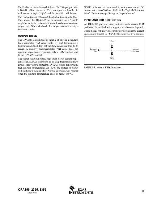
INPUT AND ESD PROTECTION<br />
All OPAx355 pins are static protected with internal ESD<br />
protection diodes tied to the supplies, as shown in Figure 1.<br />
These diodes will provide overdrive protection if the current<br />
is externally limited to 10mA by the source or by a resistor.<br />
External<br />
Pin<br />
+V CC<br />
FIGURE 1. Internal ESD Protection.<br />
Internal<br />
Circuitry<br />
–V CC<br />
<strong>OPA355</strong>, <strong>2355</strong>, <strong>3355</strong> 11<br />
SBOS195B