"OPA355,2355,3355: High Speed,Video CMOS Operational Amp."
"OPA355,2355,3355: High Speed,Video CMOS Operational Amp."
"OPA355,2355,3355: High Speed,Video CMOS Operational Amp."

Create successful ePaper yourself
Turn your PDF publications into a flip-book with our unique Google optimized e-Paper software.
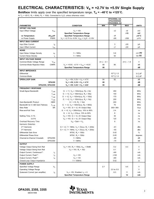
ELECTRICAL CHARACTERISTICS: V S = +2.7V to +5.5V Single Supply<br />
Boldface limits apply over the specified temperature range, T A = –40°C to +125°C.<br />
At T A = +25°C, R F = 604Ω, R L = 150Ω, Connected to V S /2, unless otherwise noted.<br />
<strong>OPA355</strong>NA, UA,<br />
OPA<strong>2355</strong>DGSA<br />
OPA<strong>3355</strong>EA, UA<br />
PARAMETER CONDITION MIN TYP MAX UNITS<br />
OFFSET VOLTAGE<br />
Input Offset Voltage V OS V S = +5V ±2 ±9 mV<br />
Specified Temperature Range ±15 mV<br />
vs Temperature dV OS /dT Specified Temperature Range ±7 µV/°C<br />
vs Power Supply PSRR V S = +2.7V to +5.5V, V CM = V S /2 – 0.15V ±80 ±350 µV/V<br />
INPUT BIAS CURRENT<br />
Input Bias Current I B 3 ±50 pA<br />
Input Offset Current I OS ±1 ±50 pA<br />
NOISE<br />
Input Noise Voltage Density e n f = 1MHz 5.8 nV/√Hz<br />
Current Noise Density i n f = 1MHz 50 fA/√Hz<br />
INPUT VOLTAGE RANGE<br />
Common-Mode Voltage Range V CM (V–) – 0.1 (V+) – 1.5 V<br />
Common-Mode Rejection Ratio CMRR V S = +5.5V, –0.1V < V CM < +4.0V 66 80 dB<br />
Specified Temperature Range 66 dB<br />
INPUT IMPEDANCE<br />
Differential 10 13 || 1.5 Ω || pF<br />
Common-Mode 10 13 || 1.5 Ω || pF<br />
OPEN-LOOP GAIN V S = +5V, 0.3V < V O < 4.7V 84 92 dB<br />
<strong>OPA355</strong> V S = +5V, 0.3V < V O < 4.7V 80 dB<br />
OPA<strong>2355</strong>, OPA<strong>3355</strong> V S = +5V, 0.4V < V O < 4.6V 80 dB<br />
FREQUENCY RESPONSE<br />
Small-Signal Bandwidth f –3dB G = +1, V O = 100mVp-p, R F = 0Ω 450 MHz<br />
f –3dB G = +2, V O = 100mVp-p, R L = 50Ω 100 MHz<br />
f –3dB G = +2, V O = 100mVp-p, R L = 150Ω 170 MHz<br />
f –3dB G = +2, V O = 100mVp-p, R L = 1kΩ 200 MHz<br />
Gain-Bandwidth Product GBW G = +10, R L = 1kΩ 200 MHz<br />
Bandwidth for 0.1dB Gain Flatness f 0.1dB G = +2, V O = 100mVp-p, R F = 560Ω 75 MHz<br />
Slew Rate SR V S = +5V, G = +2, 4V Output Step 300/–360 V/µs<br />
Rise-and-Fall Time G = +2, V O = 200mVp-p, 10% to 90% 2.4 ns<br />
G = +2, V O = 2Vp-p, 10% to 90% 8 ns<br />
Settling Time, 0.1% V S = +5V, G = +2, 2V Output Step 30 ns<br />
0.01% V S = +5V, G = +2, 2V Output Step 120 ns<br />
Overload Recovery Time V IN • Gain = V S 8 ns<br />
Harmonic Distortion<br />
2 nd Harmonic G = +2, f = 1MHz, V O = 2Vp-p, R L = 200Ω –81 dBc<br />
3 rd Harmonic G = +2, f = 1MHz, V O = 2Vp-p, R L = 200Ω –93 dBc<br />
Differential Gain Error NTSC, R L = 150Ω 0.02 %<br />
Differential Phase Error NTSC, R L = 150Ω 0.05 degrees<br />
Channel-to-Channel Crosstalk OPA<strong>2355</strong> f = 5MHz –90 dB<br />
OPA<strong>3355</strong> f = 5MHz –70 dB<br />
OUTPUT<br />
Voltage Output Swing from Rail V S = +5V, R L = 150Ω, A OL > 84dB 0.2 0.3 V<br />
Voltage Output Swing from Rail V S = +5V, R L = 1kΩ 0.1 V<br />
Output Current, Continuous (1) I O ±60 mA<br />
Output Current, Peak (1) I O V S = +5V ±100 mA<br />
Output Current, Peak (1) I O V S = +3V ±80 mA<br />
Closed-Loop Output Impedance f < 100kHz 0.02 Ω<br />
POWER SUPPLY<br />
Specified Voltage Range V S 2.7 5.5 V<br />
Operating Voltage Range 2.5 to 5.5 V<br />
Quiescent Current (per amplifier) I Q V S = +5V, Enabled, I O = 0 8.3 11 mA<br />
Specified Temperature Range 14 mA<br />
<strong>OPA355</strong>, <strong>2355</strong>, <strong>3355</strong> 3<br />
SBOS195B