Lec14
Lec14
Lec14

You also want an ePaper? Increase the reach of your titles
YUMPU automatically turns print PDFs into web optimized ePapers that Google loves.
Lecture 14:<br />
Programmable Logic Devices<br />
Objectives:<br />
• Identify programmable logic devices and understand their usage.<br />
• Understand the structure and size of the ROM, PLA and PAL<br />
• Implement Boolean functions using ROM’s, PLAs and PALs<br />
• Recognize the array logic graphic symbol and appreciate its usage in large<br />
programmable logic devices<br />
Introduction<br />
Integrated circuit categories are: SSI, MSI, LSI, and VLSI. MSI devices have a<br />
complexity of approximately 10 to 1000 ICs in a single package. Several<br />
combinational circuits are available in MSI form, e.g. adders, subtractors, decoders,<br />
encoders, multiplexers,… etc.<br />
Programmable Logic Devices are IC's with internal logic gates (arrays of AND gates<br />
and OR gates) connected through fuses to establish a pattern of connections. A<br />
typical PLD may have hundreds to millions of gates interconnected thru hundreds to<br />
thousands of internal paths.<br />
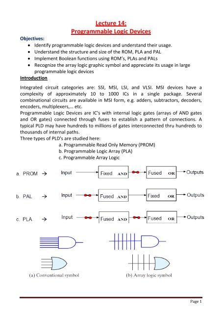
Three types of PLD's are studied here:<br />
a. Programmable Read Only Memory (PROM)<br />
b. Programmable Logic Array (PLA)<br />
c. Programmable Array Logic<br />
Page 1
Memory<br />
A memory unit is a device to which binary information is transferred for storage and<br />
from which information is retrieved when needed for processing.<br />
(a) RAM → random -access memory with both read & write operations.<br />
Examples are: Static RAM (SRAM), Dynamic RAM (DRAM).<br />
(b) ROM → read-only memory with read operation only. Examples are:<br />
PROM, EPROM, EEPROM.<br />
A memory stores information in groups of bits called words. A memory word is a<br />
group of 1s and 0s. A group of 8 bits is called a byte. Most computer memories use<br />
words that are multiple of byte. The capacity (size) of memory is usually stated as<br />
total number of bytes that the unit can store.<br />
2 10 =1K, 2 20 =1M, 1G=2 30 ……..2 16 =...K; 2 21 =...M; 2 32 =….G.<br />
“the number of address lines k is independent of the number of bits in each word”.<br />
Read Only Memory (ROM)<br />
A ROM is considered a programmable device where binary information can be stored<br />
and kept even when power supply is switched off. A ROM consists of a decoder and<br />
array of fused (programmed) OR gates. This is shown in the following Figure.<br />
Page 2
The required paths in ROM may be programmed in different ways: 1-mask<br />
programming ROM; 2-PROM; 3-EPROM (ultraviolet light); EEPROM (like flash<br />
memory)<br />
Fig. Internal logic of a 32 X 8 ROM<br />
The ROM truth table shows the pattern of the fuses as programmed inside the ROM.<br />
The following truth table is an example for the 32 X 8 ROM.<br />
Page 3
A cross indicates a connection (1), and no cross indicates (0) as shown in the<br />
following diagram.<br />
Example<br />
Design a combinational circuit using ROM that accepts a three bit number and<br />
generates an output equal to the square of the input number.<br />
All what we do is to generate a truth table for the required circuit. Most times this is<br />
all what is needed. On some occasions, we may be able to reduce the number of<br />
outputs required from the ROM.<br />
For this circuit we require six outputs, because the largest output is the binary<br />
equivalent of 7 2 = 49 →110001 2<br />
The Truth Table<br />
Page 4
Fig. PLA with three inputs, four product terms, and two outputs<br />
Combinational Circuit Implementation with PLA<br />
When implementing combinational circuit using PLA, we must reduce the number of<br />
product terms. Number of literals in each product term is not important because all<br />
variables and their complements are available.<br />
In order to reduce the number of product terms, we have to simplify the functions<br />
and their complements in order to find the combination that result in the minimum<br />
number of product terms.<br />
The size of the PLA is determined by the number of inputs, number of product terms<br />
and the number of outputs (Ex. 16x48x8).<br />
Example<br />
Implement the following two Boolean functions using a PLA.<br />
First, we simplify the functions and their complements<br />
Page 6
and<br />
and<br />
( F, F ), ( F′ , F ), ( F, F′ ), ( F′ , F′<br />
)<br />
Considering the four possible pairs 1 2 1 2 1 2 1 2<br />
The minimum number of product terms is (4) and is obtained if we implement F 1 in<br />
complement form and F2 in true form. The following PLA programming table is used.<br />
Programmable Array Logic (PAL)<br />
PAL has a fixed array of OR gates and programmable array of AND gates. It is easier<br />
to program than the PLA but is less flexible. It is suitable to implement a number of<br />
Boolean functions which have no or a few overlapping product terms.<br />
When we implement Boolean functions with PAL, we must simplify the functions to<br />
fit the sections of the PAL. A product term cannot be shared among two or more OR<br />
gates. If the function cannot fit in one section, then we may use two sections to<br />
implement the function.<br />
A typical PAL integrated circuit may have 8 inputs, 8 outputs, and 8 sections, each<br />
consisting of an 8-wide AND-OR array. The output terminals are sometimes driven by<br />
three-state buffers or inverters.<br />
The logic diagram of a typical PAL is shown in the following Figure.<br />
Page 7
3 programmable<br />
AND gates in each<br />
section and 1 OR<br />
gate<br />
Fig: PAL with 4 inputs, 4 outputs, and a 3-wide AND-OR structure.<br />
Example<br />
Implement the following Boolean functions using a PAL that has four sections with<br />
three product terms each.<br />
Page 8
Simplifying the functions results in the following functions:<br />
The PAL programming table is given below:<br />
Page 9
Page 10
FPGA<br />
Field-programmable gate array (FPGA) is a complex PAL that is configured by<br />
downloading a stream of bits into the device to configure transmission gates to<br />
establish the internal connectivity required by specified logic function (combinational<br />
or sequential).<br />
FPGA is a VLSI circuit that can be programmed at the user’s location. A typical FPGA<br />
consists of an array of hundreds or thousands of configurable logic blocks (CLBs)<br />
surrounded by programmable input and output block (IOB).<br />
A typical CLB consists of look-up tables (LUT), multiplexers, gates and flip-flops.<br />
Figure below shows a portion of the structure of an FPGA.<br />
CLB<br />
Logic module<br />
CLB<br />
Logic module<br />
Local<br />
interconnect<br />
Logic module<br />
Logic module<br />
Local<br />
interconnect<br />
Logic module<br />
Logic module<br />
Logic module<br />
Logic module<br />
Global column<br />
interconnect<br />
Global row<br />
interconnect<br />
Conclusion<br />
The design with PLD, CPLD or FPGA requires extensive computer-aided design (CAD)<br />
tools to facilitate the synthesis procedure. Among the tools that are available are<br />
schematic entry packages and HDLs such as ABEL, VHDL and Verilog.<br />
Page 11