IEEE Paper Template in A4 (V1) - ijmer
IEEE Paper Template in A4 (V1) - ijmer
IEEE Paper Template in A4 (V1) - ijmer

You also want an ePaper? Increase the reach of your titles
YUMPU automatically turns print PDFs into web optimized ePapers that Google loves.
International Journal of Modern Eng<strong>in</strong>eer<strong>in</strong>g Research (IJMER)<br />
www.<strong>ijmer</strong>.com Vol.2, Issue.1, pp-01-03 ISSN: 2249-6645<br />
Design of Operational Trans conductance Amplifier <strong>in</strong><br />
0.18μm Technology<br />
SHWETA KARNIK #1 , AJAY KUMAR KUSHWAHA #2 ,PRAMOD KUMAR JAIN #3 ,<br />
D. S. AJNAR 4 ,<br />
#1, 2, 3,4<br />
Micro Electronics and VLSI design<br />
** Electronics & Instrumentation Eng<strong>in</strong>eer<strong>in</strong>g Department, SGSITS, Indore,( M.P. )India<br />
Abstract- This paper presents design concept of Operational<br />
Transconductance Amplifier (OTA). The 0.18μm CMOS<br />
process is used for Design and Simulation of this OTA. This<br />
OTA hav<strong>in</strong>g a bias voltage 1.8 with supply voltage 1.8 V. The<br />
design and Simulation of this OTA is done us<strong>in</strong>g CADENCE<br />
Spectere environment with UMC 0.18μm technology file. The<br />
Simulation results of this OTA shows that the open loop ga<strong>in</strong><br />
of about 71 dB which hav<strong>in</strong>g GBW of 37 KHz. This OTA is<br />
hav<strong>in</strong>g CMRR of 90 dB and PSRR of 85 dB. This OTA hav<strong>in</strong>g<br />
power dissipation of 10 mW and Slew Rate 2.344 V/µsec.<br />
The Transistor M8 is an output amplifier stage. The design<br />
parameters of this OTA are shown <strong>in</strong> below table I.<br />
There are several different OTA‟s are used <strong>in</strong> which this<br />
OTA is a simple OTA with low supply voltage and high ga<strong>in</strong>.<br />
The Op-amp is characterized by various parameters like open<br />
loop ga<strong>in</strong>, Bandwidth, Slew Rate, Noise and etc. The<br />
performance Measures are fixed Due to Design parameters<br />
such as Transistors size, Bias Voltage and etc. In this paper we<br />
describe design of OTA amplifier and this design is done <strong>in</strong><br />
0.18μm technology.<br />
Keywords- OTA, Cadence, CMRR, PSRR, Power Dissipation,<br />
CMOS IC Design.<br />
1. INTRODUCTION<br />
Due to recent development <strong>in</strong> VLSI technology the size of<br />
transistors decreases and power supply also decreases. The<br />
OTA is a basic build<strong>in</strong>g block <strong>in</strong> most of analogue circuit with<br />
l<strong>in</strong>ear <strong>in</strong>put-output characteristics. The OTA is widely used <strong>in</strong><br />
analogue circuit such as neural networks, Instrumentation<br />
amplifier, ADC and Filter circuit. The operational<br />
Transconductance Amplifier (OTA) is basically similar to<br />
conventional Operational Amplifiers <strong>in</strong> which both hav<strong>in</strong>g<br />
Differential <strong>in</strong>puts. The basic difference between OTA and<br />
conventional operational Amplifier is that <strong>in</strong> OTA the output is<br />
<strong>in</strong> form of current but <strong>in</strong> conventional Op-Amps output is <strong>in</strong><br />
form of Voltage.<br />
This paper is organized as follows. Section II describes brief<br />
description about operational Transconductance Amplifier<br />
(OTA) design. Section IV describes Simulation Results of<br />
OTA. Section IV describes the conclusion of this paper.<br />
2. OPERATIONAL TRANSCONDUCTANCE<br />
AMPLIFIER (OTA) DESIGN<br />
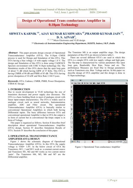
Figure 1 shows the schematic diagram of Operational<br />
Transconductance Amplifier (OTA). In this OTA the supply<br />
voltage is VDD= 1.8V. In the below circuit of OTA the<br />
Transistors, M11_1 and M11 work as a constant current source<br />
and Transistors M1, M2 and M3 works as two current mirror<br />
„pairs‟. The Transistors M4, M5, M6 and M7 are the<br />
Differential amplifier.<br />
Figure 1: Operational Tran conductance Amplifier<br />
www.<strong>ijmer</strong>.com<br />
1 | P a g e
International Journal of Modern Eng<strong>in</strong>eer<strong>in</strong>g Research (IJMER)<br />
www.<strong>ijmer</strong>.com Vol.2, Issue.1, pp-01-03 ISSN: 2249-6645<br />
TABLE I<br />
TRANSISTOR SIZE<br />
Device W/L(μm)<br />
M1,M2,M3 40/0.6<br />
M4,M5 20/0.6<br />
M6,M7,M8,M9 42/0.6<br />
M8,M9 50/0.6<br />
M10,M11 60/0.6<br />
M12,M13 0.8/0.6<br />
3. SIMULATION RESULTS<br />
The design of this Operational Transconductance Amplifier<br />
(OTA) is done us<strong>in</strong>g Cadence Tool. The Simulation results are<br />
done us<strong>in</strong>g Cadence Spectre environment us<strong>in</strong>g UMC 0.18 μm<br />
CMOS technology. The simulation result of the OTA shows<br />
that the open loop ga<strong>in</strong> of approximately 71 dB. The OTA has<br />
GBW of about 37 KHz.<br />
The Table II shows that the simulated results of the OTA. The<br />
AC response which shows ga<strong>in</strong> and phase change with<br />
frequency is shown <strong>in</strong> figure 2. Figure 3 shows the DC sweep<br />
response of This OTA. The Transient response with <strong>in</strong>put <strong>in</strong><br />
pulse is shown <strong>in</strong> figure 4. Figure 5 illustrates PSRR variations<br />
with frequency. The variation <strong>in</strong> CMRR is shown <strong>in</strong> figure 6.<br />
The simulated results of this OTA shows that PSRR of 85<br />
dB and CMRR of 90 dB.<br />
Figure 2: Shows AC response which shows ga<strong>in</strong> and phase<br />
change with frequency.<br />
TABLE II<br />
SIMULATED CHARACTERSTICS OF OTA<br />
Specifications Simulated<br />
CMOS<br />
technology<br />
Open loop ga<strong>in</strong><br />
0.18μm<br />
71 dB<br />
Figure 3: DC sweep response.<br />
Supply voltage<br />
Bias<br />
Voltage<br />
PSRR<br />
CMRR<br />
1.8 V<br />
1.8V<br />
85 dB<br />
90 dB<br />
Figure 4: Transient response with <strong>in</strong>put is pulse.<br />
www.<strong>ijmer</strong>.com<br />
2 | P a g e
International Journal of Modern Eng<strong>in</strong>eer<strong>in</strong>g Research (IJMER)<br />
www.<strong>ijmer</strong>.com Vol.2, Issue.1, pp-01-03 ISSN: 2249-6645<br />
[6] D. A. Johns and K. Mart<strong>in</strong>, Analog Integrated Circuit Design. New<br />
York: Wiley, 1997.<br />
[7] Phillip E. Allen and Douglas R. Holberg “CMOS analog circuit<br />
design” ,second edition, Oxford university press, 2007,pp. 269-274.<br />
Authors Profile:<br />
SHWETA KARNIK<br />
Figure 5: PSRR change with frequency.<br />
MTECH degree <strong>in</strong> Microelectronics and VLSI<br />
Design from SGSITS Indore 2012, work<strong>in</strong>g <strong>in</strong> the field of VLSI<br />
Design. B.E degree <strong>in</strong> Bio-Medical Eng<strong>in</strong>eer<strong>in</strong>g from Rajiv Gandhi<br />
technical university Bhopal ,INDIA <strong>in</strong> 2009.<br />
AJAY KUMAR KUSHWAHA<br />
MTECH degree <strong>in</strong> Microelectronics and VLSI<br />
Design from SGSITS Indore 2011, work<strong>in</strong>g <strong>in</strong> the field of analog<br />
design B.E. degree electronics and communication eng<strong>in</strong>eer<strong>in</strong>g from<br />
Rajiv Gandhi technical university Bhopal 2009. He is now work<strong>in</strong>g as<br />
Asst. Prof. <strong>in</strong> Department of Electronics & Communication<br />
Eng<strong>in</strong>eer<strong>in</strong>g, MITM, Indore (M.P.),<br />
Figure 6: Change <strong>in</strong> CMRR with frequency<br />
4. CONCLUSION<br />
In this paper we present a simple Operational<br />
Transconductance Amplifier (OTA) topology for low voltage<br />
and low power applications. This OTA can be used <strong>in</strong> low<br />
power, low voltage and high time constant applications such<br />
process controller, physical transducers and small battery<br />
operated devices. This work can be used <strong>in</strong> filter design, ADC<br />
design and <strong>in</strong>strumentation amplifiers because of its high ga<strong>in</strong>,<br />
high CMRR and low power consumption.<br />
5. REFERENCES<br />
[1] J. H. Botma, R.F. Wassenaar, R. J. Wieger<strong>in</strong>k, “A low voltage<br />
CMOS Op Amp with a rail-to-rail constant-gm <strong>in</strong>put stage and a class<br />
AB rail-to-rail output stage”, <strong>IEEE</strong> 1993 ISCAS, Chicago, pp.1314-<br />
1317.<br />
PRAMOD KUMAR JAIN<br />
He has received the B.E. degree <strong>in</strong> Electronics<br />
and communication Eng<strong>in</strong>eer<strong>in</strong>g from D.A.V.V. University, India <strong>in</strong><br />
1987 and M.E. Degree <strong>in</strong> Digital Techniques & Instrumentation<br />
Eng<strong>in</strong>eer<strong>in</strong>g from Rajiv Gandhi Technical University Bhopal, India<br />
<strong>in</strong>1993. He has been teach<strong>in</strong>g and <strong>in</strong> research Profession s<strong>in</strong>ce<br />
1988.He is now work<strong>in</strong>g as Reader <strong>in</strong> Department of Electronics &<br />
Instrumentation Eng<strong>in</strong>eer<strong>in</strong>g, S.G.S.I.T.S Indore, His <strong>in</strong>terest of<br />
research <strong>in</strong> Analog and digital system design.<br />
D. S. AJNAR<br />
[2] Paul R. Gray, Paul L.Hurst, Stephan H.Lewis and Robort<br />
G.Mayer “Analysis and design of analog <strong>in</strong>tegrated circuits”,Forth<br />
Edition, John Wiley & sons, <strong>in</strong>c.2001, pp.425-439.<br />
[3] Adel S. Sedra, Kenneth C.Smith “Microelectronic Circuits”,<br />
Oxford university press, Fourth edition ,2002,pp.89-91.<br />
[4] J<strong>in</strong> Tao Li, Sio Hang Pun, Peng Un Mak and Mang I Vai<br />
“Analysis of Op-Amp Power-Supply Current Sens<strong>in</strong>g Current-Mode<br />
Instrumentation Amplifier for Biosignal Acquisition System”,<strong>IEEE</strong><br />
conference,August-2008,pp.2295-2298.<br />
[5] Y. Tsividis, Operation and Model<strong>in</strong>g of the MOS Transistor, 2nd<br />
ed. Boston, MA: McGraw-Hill, 1998.<br />
He has received the B.E. degree <strong>in</strong> Electronics<br />
and Communication Eng<strong>in</strong>eer<strong>in</strong>g from D.A.V.V. University, India <strong>in</strong><br />
1993 and M.E. Degree <strong>in</strong> Digital Techniques & Instrumentation<br />
Eng<strong>in</strong>eer<strong>in</strong>g from Rajiv Gandhi Technical University Bhopal, India <strong>in</strong><br />
2000. He has been teach<strong>in</strong>g and <strong>in</strong> research Profession s<strong>in</strong>ce 1995. He<br />
is now work<strong>in</strong>g as Reader <strong>in</strong> Department of Electronics &<br />
Instrumentation Eng<strong>in</strong>eer<strong>in</strong>g, S.G.S.I.T.S Indore, India. His <strong>in</strong>terest of<br />
research is <strong>in</strong> Design<strong>in</strong>g of analog filter and Current conveyer.<br />
www.<strong>ijmer</strong>.com<br />
3 | P a g e