view full paper - Ijsrp.org
view full paper - Ijsrp.org
view full paper - Ijsrp.org

Create successful ePaper yourself
Turn your PDF publications into a flip-book with our unique Google optimized e-Paper software.
International Journal of Scientific and Research Publications, Volume 3, Issue 4, April 2013 1<br />
ISSN 2250-3153<br />
Analysis of Optical Time Division Multiplexing Using<br />
Packet Interleaving Scheme<br />
P NagaSiva Kumar, A Sangeetha, G Srikanth<br />
School of Electronics and Engineering, VIT University, Vellore<br />
Abstract- Optical time-division multiplexing (OTDM) expands and extends the well-known technique of electrical time-division<br />
multiplexing into the optical domain. In OTDM, optical data streams are constructed by time-multiplexing a number of lower bit-rate<br />
optical streams. In this <strong>paper</strong> we present an experiment work in optical time-division multiplexing and simulating a packet-interleaved<br />
operation using OptiSystem.<br />
Index Terms- Compression stage, Multiplexer, Packet interleaving scheme<br />
F<br />
I. INTRODUCTION<br />
unctionally, optical TDM (OTDM) is identical to electronic TDM. The only difference is that the multiplexing and demultiplexing<br />
operations are performed entirely optically at high speeds. At the inputs to the network, lower-speed data streams are multiplexed<br />
optically into a higher-speed data streams, and at the output of the network, the lower-speed data streams must be extracted from the<br />
higher-speed data streams optically by means of demultiplexing function. Optical signals representing data streams from multiple<br />
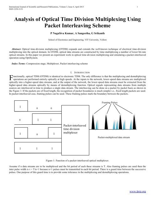
sources are interleaved in time to produce a single data stream. The interleaving can be done on a packet by packet basis as shown in<br />
the Figure 1: If the packets are of fixed length, the recognition of packet boundaries is much simpler i.e., fixed length packets are used.<br />
In packet-interleaved case, framing pulses can be used. These framing pulses mark the boundary between the packets.<br />
1<br />
11 0 0<br />
Framing Pulses<br />
0<br />
0<br />
1 1<br />
1 1<br />
Packet-interleaved<br />
time division<br />
multiplexer<br />
Packet-multiplexed data stream<br />
1 1 1<br />
Figure 1: Function of a packet-interleaved optical multiplexer.<br />
Assume if n data streams are to be multiplexed and the bit period of each these streams is T. Also framing pulses are used then the<br />
inter pulse width is τ = T/n+1 because n+1 pulses must be transmitted in each bit period. There is a guard time between the successive<br />
pulses. One purpose of this guard time is to provide some tolerance in the multiplexing and demultiplexing operations.<br />
www.ijsrp.<strong>org</strong>
International Journal of Scientific and Research Publications, Volume 3, Issue 4, April 2013 2<br />
ISSN 2250-3153<br />
II. EXPERIMENTAL SETUP<br />
In this packet interleaved case, the data stream externally modulates a periodic stream of narrow pulses. If the bit interval is T the<br />
separation between successive pulses is also T. In this way, we have to reduce the interval between successive pulses to τ, a high-rated<br />
multiplexed data signal. This is done by passing through the initial sequence through a series of compression stages as shown in<br />
Figure 2: If the size of each packet is l bits, the output goes through [k=log 2 l] compression stages. In the first compression stage, bits<br />
1,3,5,7…are delayed by T-τ. In the second compression stage, the pair of bits (1,2),(5,6),(9,10)…. are delayed by 2(T-τ). In the third<br />
compression stage, the bits (1,2,3,4),(9,10,11,12)….are delayed by 4(T-τ). Design of compression stages by using OptiSystem.<br />
T<br />
CW laser<br />
`<br />
1 1 1 1 1 1<br />
Data<br />
Modulator<br />
T-τ<br />
First<br />
compressio<br />
n stage<br />
2(T-τ)<br />
Second<br />
compressio<br />
n stage<br />
Compressed Packet<br />
Third<br />
compressio<br />
n stage<br />
Figure 2: An optical multiplexer to create a packet-interleaved TDM stream<br />
A block schematic of the four channel system is shown in Figure 3: A common 10-GHz clock drives the four transmitters via a series<br />
of micro wave delay lines that are adjusted to provide correct timing of the optical pulses. Four channels at wavelength 1550nm are<br />
RZ modulated at each 10 Gbit/s data are delayed by ¼ of the time window and then multiplexed. Total power of all channels set to -<br />
12dBm NRZ coding is a line code in which binary value ‘1’ is represented by positive voltage and ‘0’ is represented by negative<br />
voltage. The pulses have more energy than others. It requires only half the bandwidth than other coding. In RZ coding, a binary 1 is<br />
represented by first half of the bit duration, during the second half the level return to zero. Absence of a pulse represented a binary 0.<br />
Twice the bandwidth is required for RZ coding.<br />
www.ijsrp.<strong>org</strong>
International Journal of Scientific and Research Publications, Volume 3, Issue 4, April 2013 3<br />
ISSN 2250-3153<br />
4 GHZ<br />
CLOCK<br />
ELCETRICAL<br />
OPTICAL<br />
TIMING<br />
RECOVE<br />
RY<br />
ERROR<br />
TEST<br />
SET<br />
1<br />
10 Gbit/s RZ 10 Gbit/s 4 Gbit/s<br />
1<br />
τ<br />
τ<br />
2<br />
3<br />
10 Gbit/s 10 Gbit/s<br />
COMB<br />
40 Gbit/s<br />
RZ<br />
DEMU<br />
10 Gbit/s<br />
INER<br />
X<br />
10 Gbit/s<br />
FIBER<br />
2<br />
3<br />
τ<br />
DELAYS<br />
4<br />
10 Gbit/s 10 Gbit/s<br />
4<br />
TRANSMITTER<br />
RECEIVER<br />
Figure 3: Block schematic of 4-channel OTDM system.<br />
To demonstrate the packet interleaving, created a sample in which packets with 6 bits length are created. The Figure 4: shows the<br />
layout with three compression stages.<br />
Figure 4: Packet interleaving with 6bits/packet<br />
The stage was implemented in a subsystem because each compression stage has the same layout as shown in Figure 5: consist of a<br />
PRBS generator with bit rate of 10 Gbit/s and a RZ pulse generator which generates the continuous electric pulses. A light coming<br />
from a CW (Continuous Wavelength uses a Conventional band or C-band of 1550nm wavelength) laser is modulated by using AM<br />
modulator.<br />
www.ijsrp.<strong>org</strong>
International Journal of Scientific and Research Publications, Volume 3, Issue 4, April 2013 4<br />
ISSN 2250-3153<br />
Figure 5: Compression Stage<br />
There are three compression stages, the only difference between these compression stages were some parameters such as Bit rate,<br />
PRBS (Pseudo Random Bit Sequence) Generator and the Delay at the time component. The Bit rate is calculated by using<br />
Bitrate/(2 stagenumber-1 ) bits/sec and Delay is calculated by using (2 stagenumber-1 )*(1-1/pulses packet)/Bitrate.<br />
Pulse time τ (τ specifies the pulse width) = 0.06bit<br />
Pulses packet (specifies the number of bits per packet) = 6bits<br />
Bit interval T = 1bit<br />
Therefore, T-τ = 0.94 2(T-τ) = 2(0.94) 4(T-τ) = 4(0.94)……..<br />
III. RESULTS AND DISCUSSIONS<br />
The initial sequence is 11111100 and the behavior of the optical signal along the transmission can be shown in Figure 6:<br />
a<br />
b<br />
www.ijsrp.<strong>org</strong>
International Journal of Scientific and Research Publications, Volume 3, Issue 4, April 2013 5<br />
ISSN 2250-3153<br />
c<br />
Figure 6: (a) initial bit sequence (b) after 1 st compression stage (c) after 2 nd compression stage (d) after 3 rd compression stage.<br />
d<br />
Here the optical pulses are compressed at each stage as following Figure 6: In the first compression stage the bits 1,3,5,7 are<br />
compressed by T-τ , similarly the bits (1,2),(5,6), and (1,2,3,4) are compressed by 2 nd and 3 rd stages. As the use of compressing bits the<br />
bandwidth is reduced for transmitting bits.<br />
REFERENCES<br />
[1] Sachin Kumar, Indu Bala Pauria, Anoop Singhal, “ Optical Fiber Communication System Performance Using MZI Switching ”, IJSCE , Volume-2, Issue-3, July<br />
2012.<br />
[2] Jitendra Nath Roy, “Mach-Zehnder interferometer based tree architecture for all-optical logic and arithmetic operations‖”, Optik Int Light Electron Opt. (2009).<br />
[3] Rodney S.Tucker,Steven K.Korotkey,“Optical Time-Division Multiplexing For Very High Bit-Rate Transmission”. Journal of Lightwave Technology Volume-6<br />
NO.11, 1988.<br />
[4] I. Shake, H. Takara, I. Ogawa, T. Kitoh, M. Okamoto, K. Magari, T. Ohara, S. Kawanishi, “160-Gbit/s <strong>full</strong> channel optical time-division de-multiplexer based on<br />
SOA- array integrated PLC and its application to OTDM transmission experiment”, IEICE Trans. Commun. 53 (1) (2005) 20–2096B.<br />
AUTHORS<br />
First Author – P. NagaSiva Kumar, M.Tech Communications, VIT University, Vellore, (Email: siva08.444@gmail.com)<br />
Second Author – A. Sangeetha received her BE degree from Madras University and her ME degree from Madurai Kamraj University<br />
in 2000 and 2002, respectively. At present, she is working as an Assistant Professor (senior) in the School of Electronics Engineering<br />
at VIT University, Vellore, India. Her current research interest is optical OFDM. She is the author and coauthor of 9 international<br />
journal <strong>paper</strong>s and many international and national conference <strong>paper</strong>s.<br />
Third Author – G. Srikanth, M.Tech Communications, VIT University, Vellore.<br />
www.ijsrp.<strong>org</strong>