Reduction of THD in Diode Clamped Multilevel Inverter ... - Ijsrp.org
Reduction of THD in Diode Clamped Multilevel Inverter ... - Ijsrp.org
Reduction of THD in Diode Clamped Multilevel Inverter ... - Ijsrp.org

Create successful ePaper yourself
Turn your PDF publications into a flip-book with our unique Google optimized e-Paper software.
International Journal <strong>of</strong> Scientific and Research Publications, Volume 3, Issue 6, June 2013 1<br />
ISSN 2250-3153<br />
<strong>Reduction</strong> <strong>of</strong> <strong>THD</strong> <strong>in</strong> <strong>Diode</strong> <strong>Clamped</strong> <strong>Multilevel</strong> <strong>Inverter</strong><br />
employ<strong>in</strong>g SPWM technique<br />
M.Kedareswari<br />
B-tech (EEE), M-tech (PEED), Email:kedar_eee@yahoo.co.<strong>in</strong><br />
EEE Department, GNITS for women, Hyderabad, India<br />
Abstract— Conventional two-level pulse width modulation<br />
(PWM) <strong>in</strong>verters generate high dv/dt, high frequency common<br />
mode voltages and <strong>in</strong>troduces harmonics which is very harmful<br />
<strong>in</strong> electric drives applications. It may damage motor bear<strong>in</strong>gs,<br />
conducted electromagnetic <strong>in</strong>terferences, and malfunction<strong>in</strong>g <strong>of</strong><br />
electronic equipments. <strong>Multilevel</strong> <strong>in</strong>verter (MLI) technology has<br />
emerged recently as a very important alternative <strong>in</strong> the area <strong>of</strong><br />
high-power medium-voltage energy control. Neutral-po<strong>in</strong>tclamped<br />
(NPC) <strong>in</strong>verters are the most widely used topology <strong>of</strong><br />
multilevel <strong>in</strong>verters <strong>in</strong> high-power applications (several<br />
megawatts). This paper presents the most relevant control and<br />
modulation method developed for <strong>in</strong>verters to reduce total<br />
harmonic distortion (<strong>THD</strong>): multilevel s<strong>in</strong>usoidal pulse width<br />
modulation (SPWM). More relevant applications <strong>of</strong> these<br />
converters are lam<strong>in</strong>ators, conveyor belts, and unified powerflow<br />
controllers. Simulation results obta<strong>in</strong>ed <strong>in</strong> Matlab/Simul<strong>in</strong>k<br />
confirms the effectiveness with negligible <strong>THD</strong>.<br />
Index Terms- PWM, <strong>Multilevel</strong> <strong>Inverter</strong>, Neutral Po<strong>in</strong>t<br />
<strong>Clamped</strong> <strong>Inverter</strong>, Total Harmonic Distortion, SPWM.<br />
M<br />
I. INTRODUCTION<br />
ultilevel <strong>Inverter</strong>s have ga<strong>in</strong>ed much attention <strong>in</strong> the field<br />
<strong>of</strong> the medium voltage and high power applications<br />
because <strong>of</strong> their many advantages, such as their low<br />
voltage stress on power switches, low harmonic and EMI output.<br />
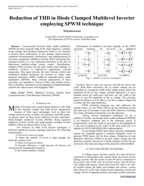
At present, there are three basic multilevel <strong>in</strong>verter topologies:<br />
diode-clamped multilevel <strong>in</strong>verter (DCMI), fly<strong>in</strong>g capacitor<br />
multilevel <strong>in</strong>verter (FCMI) and multi-module cascaded <strong>in</strong>verter<br />
(MMCI). These are shown below <strong>in</strong> Fig. 1[1].<br />
For research on multi level <strong>in</strong>verter topologies, a<br />
preferred multilevel <strong>in</strong>verter topology shall have the follow<strong>in</strong>g<br />
characteristics:<br />
1) The level is easy to extend.<br />
2) When the number <strong>of</strong> levels is high enough, the<br />
harmonic content is low.<br />
3) There is no need for filters.<br />
4) <strong>Inverter</strong> efficiency is high because all devices are<br />
switched at the fundamental frequency.<br />
5) The control method is simple.<br />
Performance <strong>of</strong> multilevel <strong>in</strong>verters depends on the PWM<br />
converter topology. In two-level or multilevel<br />
<strong>in</strong>verters, there is only one turn-on, turn-<strong>of</strong>f per device per<br />
cycle. With these converters, the ac output voltage can be<br />
controlled, by vary<strong>in</strong>g the width <strong>of</strong> the voltage pulses, and/or the<br />
amplitude <strong>of</strong> the dc bus voltage. Another approach is to have<br />
multiple pulses per half-cycle, and then vary the width <strong>of</strong> the<br />
pulses to vary the amplitude <strong>of</strong> the ac voltage. The pr<strong>in</strong>ciple<br />
reason for do<strong>in</strong>g so is to be able to vary the ac output voltage and<br />
to reduce the low-order harmonics.<br />
PWM switch<strong>in</strong>g strategies not only addresses the<br />
primary issues viz, less <strong>THD</strong>, effective dc bus utilization etc but<br />
also take care <strong>of</strong> secondary issues like EMI reduction, switch<strong>in</strong>g<br />
loss, better spread<strong>in</strong>g <strong>of</strong> harmonics over the spectrum.<br />
Among various modulation techniques [1] for a<br />
multilevel <strong>in</strong>verter, s<strong>in</strong>-triangle pulse width modulation (SPWM)<br />
is an attractive candidate due to the follow<strong>in</strong>g merits. It<br />
proportionally varies the width <strong>of</strong> each pulse to the amplitude <strong>of</strong><br />
a s<strong>in</strong>e wave evaluated at the center <strong>of</strong> the same pulse [2]. It is<br />
suitable for MATLAB/SIMULINK implementation.<br />
In s<strong>in</strong>-triangle PWM, three phase reference modulat<strong>in</strong>g<br />
signals are compared aga<strong>in</strong>st a common triangular carrier to<br />
generate PWM pulses for the three phases. <strong>Reduction</strong> <strong>of</strong> total<br />
harmonics distortion (<strong>THD</strong>) <strong>of</strong> <strong>in</strong>verter output voltage and the<br />
distortion seamless when level <strong>of</strong> diode-clamped <strong>in</strong>verter has got<br />
<strong>in</strong>creased is the ma<strong>in</strong> advantage <strong>of</strong> the proposed control method.<br />
II. VOLTAGE SOURCE INVERTERS<br />
A voltage source <strong>in</strong>verter consists <strong>of</strong> a turn-<strong>of</strong>f device<br />
connected <strong>in</strong> anti-parallel with a diode which has lowest reverse<br />
leakage current with the anode <strong>of</strong> turn-<strong>of</strong>f device connected to<br />
the positive side <strong>of</strong> DC side. In <strong>in</strong>verter action, turn-<strong>of</strong>f device<br />
will conduct and current / power flows from DC side to AC side.<br />
In rectifier action, the diode will conduct and current / power<br />
flows from AC to DC side. Under <strong>in</strong>verter operation, current and<br />
voltage will be <strong>of</strong> opposite polarity and under rectifier operation<br />
www.ijsrp.<strong>org</strong>
International Journal <strong>of</strong> Scientific and Research Publications, Volume 3, Issue 6, June 2013 2<br />
ISSN 2250-3153<br />
they will be <strong>of</strong> same polarity. The compensation is applied at<br />
mid-po<strong>in</strong>t to improve the voltage regulation. For radial l<strong>in</strong>es,<br />
shunt compensation is applied at the end <strong>of</strong> l<strong>in</strong>e to prevent<br />
voltage <strong>in</strong>stability, for dynamic voltage control, to <strong>in</strong>crease<br />
transient stability and for damp<strong>in</strong>g <strong>of</strong> power oscillations. Midpo<strong>in</strong>t<br />
<strong>of</strong> transmission l<strong>in</strong>e is the best location for compensator<br />
because the voltage sag for uncompensated l<strong>in</strong>e is maximum at<br />
the mid-po<strong>in</strong>t. Also, the compensation at mid-po<strong>in</strong>t breaks the<br />
l<strong>in</strong>e <strong>in</strong>to equal segments, for each <strong>of</strong> which, the maximum<br />
transmittable power is the same.<br />
III. INVERTER TOPOLOGY<br />
Neutral Po<strong>in</strong>t-<strong>Clamped</strong> <strong>Inverter</strong>:<br />
A three-level diode-clamped <strong>in</strong>verter is shown <strong>in</strong> Fig.<br />
2(a). In this circuit, the dc-bus voltage is split <strong>in</strong>to three levels by<br />
two series-connected bulk capacitors, C 1 and C 2 . The middle<br />
po<strong>in</strong>t <strong>of</strong> the two capacitors n can be def<strong>in</strong>ed as the neutral po<strong>in</strong>t.<br />
The output voltage v an has three states: V dc /2, 0, and -V dc /2. For<br />
voltage level V dc /2, switches S 1 and S 2 need to be turned on; for -<br />
V dc /2, switches S 1 ’ and S 2 ’ need to be turned on; and for the 0<br />
level, S 2 and S 1 ’ need to be turned on.<br />
The key components that dist<strong>in</strong>guish this circuit from a<br />
conventional two-level <strong>in</strong>verter are D 1 and D 1 ’. These two diodes<br />
clamp the switch voltage to half the level <strong>of</strong> the dc-bus voltage.<br />
When both S 1 and S 2 turn on, the voltage across a and 0 is V dc<br />
i.e., v a0 =V dc . In this case, D 1 ’ balances out the voltage shar<strong>in</strong>g<br />
between S 1 ’ and S 2 ’ with S 1 ’ block<strong>in</strong>g the voltage across C 1 and<br />
S 2 ’ block<strong>in</strong>g the voltage across C 2 . Notice that output voltage v an<br />
is ac, and v a0 is dc. The difference between v an and v a0 is the<br />
voltage across C 2 , which is V dc /2. If the output is removed out<br />
between a and 0, then the circuit becomes a dc/dc converter,<br />
which has three output voltage levels: V dc , V dc /2, and 0.<br />
distortion. However, a high number <strong>of</strong> levels <strong>in</strong>creases the<br />
control complexity and <strong>in</strong>troduces voltage imbalance problems.<br />
Fig. 2(b) shows a five-level diode-clamped converter <strong>in</strong><br />
which the dc bus consists <strong>of</strong> four capacitors, C 1 , C 2 , C 3 , and C 4 .<br />
For dc-bus voltage V dc , the voltage across each capacitor is V dc /4,<br />
and each device voltage stress will be limited to one capacitor<br />
voltage level V dc /4 through clamp<strong>in</strong>g diodes.<br />
To expla<strong>in</strong> how the staircase voltage is synthesized, the<br />
neutral po<strong>in</strong>t n is considered as the output phase voltage<br />
reference po<strong>in</strong>t. There are five switch comb<strong>in</strong>ations to synthesize<br />
five level voltages across a and n.<br />
1) For voltage level V an = V dc /2, turn on all upper switches<br />
S 1 – S 4 .<br />
2) For voltage level V an = V dc /4, turn on three upper switches<br />
S 2 – S 4 and one lower switch S 1 ’.<br />
3) For voltage level V an = 0, turn on two upper switches<br />
S 3 and S 4 and two lower switches S 1 ’ and S 2 ’.<br />
4) For voltage level V an = –V dc /4, turn on one upper switch<br />
and three lower switches S 1 ’– S 3 ’.<br />
5) For voltage level V an = –V dc /2, turn on all lower switches<br />
S 1 ’– S 4 ’.<br />
Four complementary switch pairs exist <strong>in</strong> each phase. The<br />
complementary switch pair is def<strong>in</strong>ed such that turn<strong>in</strong>g on one <strong>of</strong><br />
the switches will exclude the other from be<strong>in</strong>g turned on. In this<br />
example, the four complementary pairs are (S 1 , S 1 ’), (S 2 , S 2 ’), (S 3 ,<br />
S 3 ’), and (S 4 , S 4 ’).<br />
TABLE I. SWITHCING STATES OF THE FIVE LEVEL INVERTER<br />
Output<br />
v a0<br />
Switch States<br />
S 1 S 2 S 3 S 4 S 1 ’ S 2 ’ S 3 ’ S 4 ’<br />
V5=Vdc<br />
1 1 1 1 0 0 0 0<br />
V4=3Vdc/4<br />
0 1 1 1 1 0 0 0<br />
V3=Vdc/2<br />
0 0 1 1 1 1 0 0<br />
V2=Vdc/4<br />
0 0 0 1 1 1 1 0<br />
V1= 0<br />
0 0 0 0 1 1 1 1<br />
Fig. 2. <strong>Diode</strong>clamped<br />
multilevel <strong>in</strong>verter circuit topologies.<br />
(a) Three-level. (b) Five-level.<br />
Consider<strong>in</strong>g that m is the number <strong>of</strong> steps <strong>of</strong> the phase voltage<br />
with respect to the negative term<strong>in</strong>al <strong>of</strong> the <strong>in</strong>verter, then the<br />
number <strong>of</strong> steps <strong>in</strong> the voltage between two phases <strong>of</strong> the load k<br />
is<br />
k = 2m+1<br />
(1) and the<br />
number <strong>of</strong> steps p <strong>in</strong> the phase voltage <strong>of</strong> a three-phase load <strong>in</strong><br />
wye connection is<br />
p = 2k – 1. (2)<br />
The term multilevel starts with the three-level <strong>in</strong>verter<br />
<strong>in</strong>troduced by Nabae et al. [3]. By <strong>in</strong>creas<strong>in</strong>g the number <strong>of</strong><br />
levels <strong>in</strong> the <strong>in</strong>verter, the output voltages have more steps<br />
generat<strong>in</strong>g a staircase waveform, which has a reduced harmonic<br />
Although each active switch<strong>in</strong>g device is only required<br />
to block a voltage level <strong>of</strong> V dc /(m-1), the clamp<strong>in</strong>g diodes must<br />
have different voltage rat<strong>in</strong>gs for reverse voltage block<strong>in</strong>g. Us<strong>in</strong>g<br />
D 1 ’<strong>of</strong> Fig. 2(b) as an example, when lower devices S 2 ’ ~ S 4 ’ are<br />
turned on, D 1 ’ needs to block three capacitor voltages, or 3V dc /4.<br />
Similarly, D 2 and D 2 ’ need to block 2V dc /4, and D 3 needs to block<br />
3V dc /4. Assum<strong>in</strong>g that each block<strong>in</strong>g diode voltage rat<strong>in</strong>g is the<br />
same as the active device voltage rat<strong>in</strong>g, the number <strong>of</strong> diodes<br />
required for each phase will be (m-1) (m-2). This number<br />
represents a quadratic <strong>in</strong>crease <strong>in</strong> m. When m is sufficiently high,<br />
the number <strong>of</strong> diodes required will make the system impractical<br />
to implement. If the <strong>in</strong>verter runs under PWM, the diode reverse<br />
recovery <strong>of</strong> these clamp<strong>in</strong>g diodes becomes the major design<br />
challenge <strong>in</strong> high-voltage high-power applications.<br />
IV. CONTROL STRATEGY<br />
In many <strong>in</strong>dustrial applications, to control <strong>of</strong> the output<br />
voltage <strong>of</strong> <strong>in</strong>verters is <strong>of</strong>ten necessary to cope with the variations<br />
<strong>of</strong> dc <strong>in</strong>put voltage, to regulate <strong>of</strong> <strong>in</strong>verters and to satisfy the<br />
constant volts and frequency control requirement. There are<br />
various techniques to vary the <strong>in</strong>verter ga<strong>in</strong>. The most efficient<br />
www.ijsrp.<strong>org</strong>
International Journal <strong>of</strong> Scientific and Research Publications, Volume 3, Issue 6, June 2013 3<br />
ISSN 2250-3153<br />
method <strong>of</strong> controll<strong>in</strong>g the ga<strong>in</strong> and output voltage is to<br />
<strong>in</strong>corporate PWM control with<strong>in</strong> the <strong>in</strong>verters.<br />
The modulation methods used <strong>in</strong> multilevel <strong>in</strong>verters<br />
can be classified accord<strong>in</strong>g to switch<strong>in</strong>g frequency [4], [5].<br />
Methods that work with low switch<strong>in</strong>g frequencies generally<br />
perform one or two commutations <strong>of</strong> the power semiconductors<br />
dur<strong>in</strong>g one cycle <strong>of</strong> the output voltages, generat<strong>in</strong>g a staircase<br />
waveform.<br />
Methods that work with high switch<strong>in</strong>g frequencies<br />
have many commutations for the power semiconductors <strong>in</strong> one<br />
period <strong>of</strong> the fundamental output voltage. A very popular method<br />
<strong>in</strong> <strong>in</strong>dustrial applications is the classic carrier-based s<strong>in</strong>usoidal<br />
PWM (SPWM) that uses the phase-shift<strong>in</strong>g technique to reduce<br />
the harmonics <strong>in</strong> the load voltage [6].<br />
SPWM:<br />
V. PROPOSED TECHNIQUE<br />
Several multicarrier techniques have been developed to<br />
reduce the distortion <strong>in</strong> multilevel <strong>in</strong>verters, based on the<br />
classical SPWM with triangular carriers. Some methods use<br />
carrier disposition and others use phase shift<strong>in</strong>g <strong>of</strong> multiple<br />
carrier signals [7], [8], [9].<br />
The s<strong>in</strong>usoidal PWM compares a high frequency<br />
triangular carrier with three s<strong>in</strong>usoidal reference signals, known<br />
as the modulat<strong>in</strong>g signals to generate the gat<strong>in</strong>g signals for the<br />
<strong>in</strong>verter switches. This is basically an analog doma<strong>in</strong> technique<br />
and is commonly used <strong>in</strong> power conversion with both analog and<br />
digital implementation.<br />
The smallest distortion is obta<strong>in</strong>ed when the carriers are<br />
shifted by an angle <strong>of</strong><br />
. A very common<br />
practice <strong>in</strong> <strong>in</strong>dustrial applications for the multilevel <strong>in</strong>verter is the<br />
<strong>in</strong>jection <strong>of</strong> a third harmonic <strong>in</strong> each cell to <strong>in</strong>crease the output<br />
voltage [6], [10]. Another advantageous feature <strong>of</strong> multilevel<br />
SPWM is that the effective switch<strong>in</strong>g frequency <strong>of</strong> the load<br />
voltage is three (N C =3) times the switch<strong>in</strong>g frequency <strong>of</strong> each<br />
cell, as determ<strong>in</strong>ed by its carrier signal. This property allows a<br />
reduction <strong>in</strong> the switch<strong>in</strong>g frequency <strong>of</strong> each cell, thus reduc<strong>in</strong>g<br />
the switch<strong>in</strong>g losses.<br />
To verify the proposed scheme, MATLAB/SIMULINK<br />
s<strong>of</strong>tware is implemented. The experimental results are presented<br />
for different levels <strong>of</strong> NPCI us<strong>in</strong>g s<strong>in</strong>usoidal PWM technique. In<br />
SPWM control the pulse widths are generated by compar<strong>in</strong>g a<br />
triangular reference signal with carrier s<strong>in</strong>usoidal signal. And<br />
these generated pulses are given for all switch<strong>in</strong>g devices <strong>of</strong><br />
proposed <strong>in</strong>verter. DC voltage <strong>of</strong> the <strong>in</strong>verter for three level is<br />
E=100V and for five level E=440V. Fig 5.1 shows the reference<br />
signal is compared with two (3-1) carrier signals to generate<br />
three level output. Similarly Fig 5.4 shows the comparison with<br />
four (5-1) carrier signals to generate five level output. Fig. 5.2<br />
illustrates the l<strong>in</strong>e voltage <strong>of</strong> NPC three level <strong>in</strong>verter with<br />
SPWM and Fig. 5.3 illustrates the <strong>THD</strong> spectrum <strong>of</strong> NPC three<br />
level <strong>in</strong>verter with SPWM. In this modulation technique the <strong>THD</strong><br />
is 34.51%. Fig. 5.5 illustrates the l<strong>in</strong>e voltage <strong>of</strong> NPC five level<br />
<strong>in</strong>verter with SPWM and Fig. 5.6 illustrates the <strong>THD</strong> spectrum <strong>of</strong><br />
NPC five level <strong>in</strong>verter with SPWM. In this modulation<br />
technique the <strong>THD</strong> is 16.82%.<br />
The output voltage is closer to s<strong>in</strong>usoid and the <strong>THD</strong><br />
values <strong>of</strong> l<strong>in</strong>e voltages also seamless as the level <strong>in</strong>creases.<br />
Fig. 5.1 The reference (cos<strong>in</strong>e) and carrier waves (triangular) for a three-level<br />
NPCMLI with SPWM.<br />
Proposed SPWM for NPC <strong>Multilevel</strong> <strong>Inverter</strong>:<br />
In the SPWM scheme for two-level <strong>in</strong>verters, each<br />
reference phase voltage is compared with the triangular carrier<br />
and the <strong>in</strong>dividual pole voltages are generated, <strong>in</strong>dependent <strong>of</strong><br />
each other. The SPWM technique, for multilevel <strong>in</strong>verters,<br />
<strong>in</strong>volves compar<strong>in</strong>g the reference phase voltage signals with a<br />
number <strong>of</strong> symmetrical level-shifted carrier waves for PWM<br />
generation [11]. It has been shown that for an n-level <strong>in</strong>verter, n-<br />
1 level-shifted carrier waves are required for comparison with the<br />
s<strong>in</strong>usoidal references [11].<br />
When used for an NPCMLI with n number <strong>of</strong> voltage<br />
levels, n-1 number <strong>of</strong> triangular carrier waves is used. These<br />
carrier waves have the same frequency and are arranged on top<br />
<strong>of</strong> each other, so that they together span from maximum output<br />
voltage to m<strong>in</strong>imum output voltage [12]. When one carrier wave<br />
is crossed by the reference the output wave steps one level up or<br />
down with a switch transaction.<br />
VI. SIMULATION RESULTS<br />
Fig. 5.2 The output voltage for a Three-level NPCMLI with SPWM.<br />
Fig. 5.3 <strong>THD</strong> spectrum for a three-level NPCMLI with SPWM<br />
www.ijsrp.<strong>org</strong>
International Journal <strong>of</strong> Scientific and Research Publications, Volume 3, Issue 6, June 2013 4<br />
ISSN 2250-3153<br />
any multilevel <strong>in</strong>verter configurations and we can generalize this<br />
method to any higher order <strong>in</strong>verters.<br />
REFERENCES<br />
Fig. 5.4 The reference (cos<strong>in</strong>e) and carrier waves (triangular) for a five-level<br />
NPCMLI with SPWM.<br />
Fig. 5.5 The reference (cos<strong>in</strong>e) and carrier waves (triangular) for a five-level<br />
NPCMLI with SPWM.<br />
[1] J. Rodriguez, J. S. Lai, and F. Z. Peng, “<strong>Multilevel</strong> <strong>in</strong>verters: A survey <strong>of</strong><br />
topologies, controls, and applications,” IEEE Trans. Ind. Electron., vol. 49, no.<br />
4, pp. 724–738, Aug. 2002.<br />
[2] T.Ohnishi and H.Okitsu, “A novel PWM technique for three-phase<br />
<strong>in</strong>verter/converter,” International Power Electronics Conference, 1983, pp.384-<br />
395.<br />
[3] A. Nabae, I. Takahashi, and H. Akagi, “A new neutral-po<strong>in</strong>t clamped PWM<br />
<strong>in</strong>verter,” IEEE Trans. Ind. Applicat., vol. IA-17, pp. 518–523, Sept./Oct. 1981.<br />
[4] N. Celanovic and D. Boroyevic, “A fast space vector modulation algorithm<br />
for multilevel three-phase converters,” <strong>in</strong> Conf. Rec. IEEE-IAS Annu. Meet<strong>in</strong>g,<br />
Phoenix, AZ, Oct. 1999, pp. 1173–1177.<br />
[5] J. Rodríguez, P. Correa, and L. Morán, “A vector control technique for<br />
medium voltage multilevel <strong>in</strong>verters,” <strong>in</strong> Proc. IEEE APEC, Anaheim, CA, Mar.<br />
2001, pp. 173–178.<br />
[6] P. Hammond, “A new approach to enhance power quality for medium voltage<br />
ac drives,” IEEE Trans. Ind. Applicat., vol. 33, pp. 202–208, Jan./Feb. 1997.<br />
[7] L. Tolbert and T. G. Habetler, “Novel multilevel <strong>in</strong>verter carrier-based PWM<br />
method,” IEEE Trans. Ind. Applicat., vol. 35, pp. 1098–1107, Sept./Oct. 1999.<br />
[8] B. N. Mw<strong>in</strong>yiwiwa, Z.Wolanski, and B. T. Ooi, “Microprocessor<br />
implemented SPWM for multiconverters with phase-shifted triangle carriers,” <strong>in</strong><br />
Conf. Rec. IEEE-IAS Annu. Meet<strong>in</strong>g, NewOrleans, LA, Oct. 1997, pp. 1542–<br />
1549.<br />
[9] V. G. Agelidis and M. Calais, “Application specific harmonic performance<br />
evaluation <strong>of</strong> multicarrier PWM techniques,” <strong>in</strong> Proc. IEEE PESC’98, Fukuoka,<br />
Japan, May 1998, pp. 172–178.<br />
[10] W. A. Hill and C. D. Harbourt, “Performance <strong>of</strong> medium voltage multilevel<br />
<strong>in</strong>verters,” <strong>in</strong> Conf. Rec. IEEE-IAS Annu. Meet<strong>in</strong>g, Pheonix, AZ, Oct. 1999, pp.<br />
1186–1192.<br />
[11] Carrara, G.,Gardella, S.G., Archesoni,M., Salutari, R., and Sciutto,<br />
G.: ‘A new multi-level PWM method: A theoretical analysis’, IEEE Trans.<br />
Power Electron., 1992, 7, (3), pp. 497–505<br />
[12] McGrath, B.P.; Holmes, D.G.; "Multicarrier PWM strategies for multilevel<br />
<strong>in</strong>verters," Industrial Electronics, IEEE Transactions on, vol.49, no.4, pp. 858-<br />
867, Aug 2002 doi: 10.1109/TIE.2002.801073<br />
Fig. 5.6 <strong>THD</strong> spectrum for a three-level NPCMLI with SPWM<br />
TABLE II. REDUCTION OF <strong>THD</strong> BY VARYING INVERTER LEVEL<br />
Output Voltage level<br />
<strong>of</strong> NPCI<br />
<strong>THD</strong><br />
Fundamental<br />
Component<br />
Three Level 34.51% 84.45<br />
Five Level 16.82% 347<br />
VII. CONCLUSION<br />
A classical SPWM technique is proposed for three-level<br />
and five-level NPC <strong>in</strong>verter. The ma<strong>in</strong> feature <strong>of</strong> the modulation<br />
scheme lies <strong>in</strong> its ability to elim<strong>in</strong>ate the harmonics <strong>in</strong> the<br />
<strong>in</strong>verter output voltages. To assist the analysis and design <strong>of</strong> the<br />
classical scheme, the mechanism <strong>of</strong> the <strong>THD</strong> reduction with<br />
<strong>in</strong>crease <strong>in</strong> level <strong>of</strong> <strong>in</strong>verter employ<strong>in</strong>g SPWM technique is<br />
discussed.<br />
The harmonic content and <strong>THD</strong> <strong>of</strong> the <strong>in</strong>verter output voltage<br />
produced by the three and five levels are compared and it<br />
seamless for five level neutral po<strong>in</strong>t clamped <strong>in</strong>verter compared<br />
to three level NPCI. The proposed technique can be applied to<br />
www.ijsrp.<strong>org</strong>