view full paper - Ijsrp.org
view full paper - Ijsrp.org
view full paper - Ijsrp.org

You also want an ePaper? Increase the reach of your titles
YUMPU automatically turns print PDFs into web optimized ePapers that Google loves.
International Journal of Scientific and Research Publications, Volume 3, Issue 4, April 2013 1<br />
ISSN 2250-3153<br />
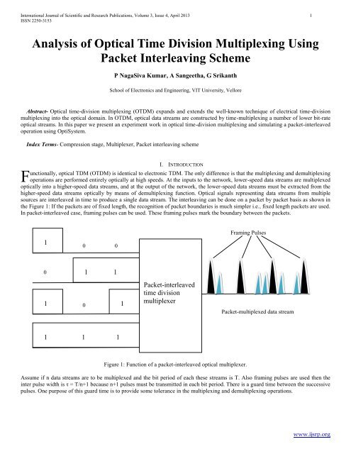
Analysis of Optical Time Division Multiplexing Using<br />
Packet Interleaving Scheme<br />
P NagaSiva Kumar, A Sangeetha, G Srikanth<br />
School of Electronics and Engineering, VIT University, Vellore<br />
Abstract- Optical time-division multiplexing (OTDM) expands and extends the well-known technique of electrical time-division<br />
multiplexing into the optical domain. In OTDM, optical data streams are constructed by time-multiplexing a number of lower bit-rate<br />
optical streams. In this <strong>paper</strong> we present an experiment work in optical time-division multiplexing and simulating a packet-interleaved<br />
operation using OptiSystem.<br />
Index Terms- Compression stage, Multiplexer, Packet interleaving scheme<br />
F<br />
I. INTRODUCTION<br />
unctionally, optical TDM (OTDM) is identical to electronic TDM. The only difference is that the multiplexing and demultiplexing<br />
operations are performed entirely optically at high speeds. At the inputs to the network, lower-speed data streams are multiplexed<br />
optically into a higher-speed data streams, and at the output of the network, the lower-speed data streams must be extracted from the<br />
higher-speed data streams optically by means of demultiplexing function. Optical signals representing data streams from multiple<br />
sources are interleaved in time to produce a single data stream. The interleaving can be done on a packet by packet basis as shown in<br />
the Figure 1: If the packets are of fixed length, the recognition of packet boundaries is much simpler i.e., fixed length packets are used.<br />
In packet-interleaved case, framing pulses can be used. These framing pulses mark the boundary between the packets.<br />
1<br />
11 0 0<br />
Framing Pulses<br />
0<br />
0<br />
1 1<br />
1 1<br />
Packet-interleaved<br />
time division<br />
multiplexer<br />
Packet-multiplexed data stream<br />
1 1 1<br />
Figure 1: Function of a packet-interleaved optical multiplexer.<br />
Assume if n data streams are to be multiplexed and the bit period of each these streams is T. Also framing pulses are used then the<br />
inter pulse width is τ = T/n+1 because n+1 pulses must be transmitted in each bit period. There is a guard time between the successive<br />
pulses. One purpose of this guard time is to provide some tolerance in the multiplexing and demultiplexing operations.<br />
www.ijsrp.<strong>org</strong>
International Journal of Scientific and Research Publications, Volume 3, Issue 4, April 2013 2<br />
ISSN 2250-3153<br />
II. EXPERIMENTAL SETUP<br />
In this packet interleaved case, the data stream externally modulates a periodic stream of narrow pulses. If the bit interval is T the<br />
separation between successive pulses is also T. In this way, we have to reduce the interval between successive pulses to τ, a high-rated<br />
multiplexed data signal. This is done by passing through the initial sequence through a series of compression stages as shown in<br />
Figure 2: If the size of each packet is l bits, the output goes through [k=log 2 l] compression stages. In the first compression stage, bits<br />
1,3,5,7…are delayed by T-τ. In the second compression stage, the pair of bits (1,2),(5,6),(9,10)…. are delayed by 2(T-τ). In the third<br />
compression stage, the bits (1,2,3,4),(9,10,11,12)….are delayed by 4(T-τ). Design of compression stages by using OptiSystem.<br />
T<br />
CW laser<br />
`<br />
1 1 1 1 1 1<br />
Data<br />
Modulator<br />
T-τ<br />
First<br />
compressio<br />
n stage<br />
2(T-τ)<br />
Second<br />
compressio<br />
n stage<br />
Compressed Packet<br />
Third<br />
compressio<br />
n stage<br />
Figure 2: An optical multiplexer to create a packet-interleaved TDM stream<br />
A block schematic of the four channel system is shown in Figure 3: A common 10-GHz clock drives the four transmitters via a series<br />
of micro wave delay lines that are adjusted to provide correct timing of the optical pulses. Four channels at wavelength 1550nm are<br />
RZ modulated at each 10 Gbit/s data are delayed by ¼ of the time window and then multiplexed. Total power of all channels set to -<br />
12dBm NRZ coding is a line code in which binary value ‘1’ is represented by positive voltage and ‘0’ is represented by negative<br />
voltage. The pulses have more energy than others. It requires only half the bandwidth than other coding. In RZ coding, a binary 1 is<br />
represented by first half of the bit duration, during the second half the level return to zero. Absence of a pulse represented a binary 0.<br />
Twice the bandwidth is required for RZ coding.<br />
www.ijsrp.<strong>org</strong>
International Journal of Scientific and Research Publications, Volume 3, Issue 4, April 2013 3<br />
ISSN 2250-3153<br />
4 GHZ<br />
CLOCK<br />
ELCETRICAL<br />
OPTICAL<br />
TIMING<br />
RECOVE<br />
RY<br />
ERROR<br />
TEST<br />
SET<br />
1<br />
10 Gbit/s RZ 10 Gbit/s 4 Gbit/s<br />
1<br />
τ<br />
τ<br />
2<br />
3<br />
10 Gbit/s 10 Gbit/s<br />
COMB<br />
40 Gbit/s<br />
RZ<br />
DEMU<br />
10 Gbit/s<br />
INER<br />
X<br />
10 Gbit/s<br />
FIBER<br />
2<br />
3<br />
τ<br />
DELAYS<br />
4<br />
10 Gbit/s 10 Gbit/s<br />
4<br />
TRANSMITTER<br />
RECEIVER<br />
Figure 3: Block schematic of 4-channel OTDM system.<br />
To demonstrate the packet interleaving, created a sample in which packets with 6 bits length are created. The Figure 4: shows the<br />
layout with three compression stages.<br />
Figure 4: Packet interleaving with 6bits/packet<br />
The stage was implemented in a subsystem because each compression stage has the same layout as shown in Figure 5: consist of a<br />
PRBS generator with bit rate of 10 Gbit/s and a RZ pulse generator which generates the continuous electric pulses. A light coming<br />
from a CW (Continuous Wavelength uses a Conventional band or C-band of 1550nm wavelength) laser is modulated by using AM<br />
modulator.<br />
www.ijsrp.<strong>org</strong>
International Journal of Scientific and Research Publications, Volume 3, Issue 4, April 2013 4<br />
ISSN 2250-3153<br />
Figure 5: Compression Stage<br />
There are three compression stages, the only difference between these compression stages were some parameters such as Bit rate,<br />
PRBS (Pseudo Random Bit Sequence) Generator and the Delay at the time component. The Bit rate is calculated by using<br />
Bitrate/(2 stagenumber-1 ) bits/sec and Delay is calculated by using (2 stagenumber-1 )*(1-1/pulses packet)/Bitrate.<br />
Pulse time τ (τ specifies the pulse width) = 0.06bit<br />
Pulses packet (specifies the number of bits per packet) = 6bits<br />
Bit interval T = 1bit<br />
Therefore, T-τ = 0.94 2(T-τ) = 2(0.94) 4(T-τ) = 4(0.94)……..<br />
III. RESULTS AND DISCUSSIONS<br />
The initial sequence is 11111100 and the behavior of the optical signal along the transmission can be shown in Figure 6:<br />
a<br />
b<br />
www.ijsrp.<strong>org</strong>
International Journal of Scientific and Research Publications, Volume 3, Issue 4, April 2013 5<br />
ISSN 2250-3153<br />
c<br />
Figure 6: (a) initial bit sequence (b) after 1 st compression stage (c) after 2 nd compression stage (d) after 3 rd compression stage.<br />
d<br />
Here the optical pulses are compressed at each stage as following Figure 6: In the first compression stage the bits 1,3,5,7 are<br />
compressed by T-τ , similarly the bits (1,2),(5,6), and (1,2,3,4) are compressed by 2 nd and 3 rd stages. As the use of compressing bits the<br />
bandwidth is reduced for transmitting bits.<br />
REFERENCES<br />
[1] Sachin Kumar, Indu Bala Pauria, Anoop Singhal, “ Optical Fiber Communication System Performance Using MZI Switching ”, IJSCE , Volume-2, Issue-3, July<br />
2012.<br />
[2] Jitendra Nath Roy, “Mach-Zehnder interferometer based tree architecture for all-optical logic and arithmetic operations‖”, Optik Int Light Electron Opt. (2009).<br />
[3] Rodney S.Tucker,Steven K.Korotkey,“Optical Time-Division Multiplexing For Very High Bit-Rate Transmission”. Journal of Lightwave Technology Volume-6<br />
NO.11, 1988.<br />
[4] I. Shake, H. Takara, I. Ogawa, T. Kitoh, M. Okamoto, K. Magari, T. Ohara, S. Kawanishi, “160-Gbit/s <strong>full</strong> channel optical time-division de-multiplexer based on<br />
SOA- array integrated PLC and its application to OTDM transmission experiment”, IEICE Trans. Commun. 53 (1) (2005) 20–2096B.<br />
AUTHORS<br />
First Author – P. NagaSiva Kumar, M.Tech Communications, VIT University, Vellore, (Email: siva08.444@gmail.com)<br />
Second Author – A. Sangeetha received her BE degree from Madras University and her ME degree from Madurai Kamraj University<br />
in 2000 and 2002, respectively. At present, she is working as an Assistant Professor (senior) in the School of Electronics Engineering<br />
at VIT University, Vellore, India. Her current research interest is optical OFDM. She is the author and coauthor of 9 international<br />
journal <strong>paper</strong>s and many international and national conference <strong>paper</strong>s.<br />
Third Author – G. Srikanth, M.Tech Communications, VIT University, Vellore.<br />
www.ijsrp.<strong>org</strong>