TSV technology for large die Cu/low K chip packaging
TSV technology for large die Cu/low K chip packaging
TSV technology for large die Cu/low K chip packaging

You also want an ePaper? Increase the reach of your titles
YUMPU automatically turns print PDFs into web optimized ePapers that Google loves.
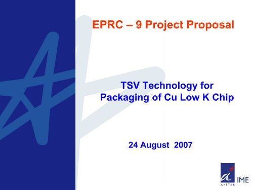
EPRC – 9 Project Proposal<br />
<strong>TSV</strong> Technology <strong>for</strong><br />
Packaging of <strong>Cu</strong> Low K Chip<br />
24 August 2007
Introduction<br />
Background<br />
• <strong>Cu</strong> <strong>low</strong>-K <strong>technology</strong> is moving towards finer feature and newer Low K materials<br />
• 90nm 65nm 45nm <strong>technology</strong> with <strong>Cu</strong>-<strong>low</strong> K Ultra <strong>low</strong> K materials<br />
• Higher per<strong>for</strong>mance <strong>chip</strong> require higher I/O, finer pitch, <strong>large</strong>r <strong>chip</strong> size<br />
• Bottle neck: Feature size of build up substrate can not keep pace with device trend<br />
• Concern: Assembly, materials and reliability impact on the 45nm <strong>Cu</strong> / Ultra <strong>low</strong> K <strong>chip</strong><br />
is not well understood<br />
• A solution to realize <strong>low</strong> stress <strong>packaging</strong> and high density interconnection is needed<br />
• IME has capabilities in related technologies<br />
• <strong>Cu</strong> <strong>low</strong> K <strong>packaging</strong> with 150um bump pitch, Pb free solder and organic BU substrate<br />
• Core competencies in Thru-Silicon-Via (<strong>TSV</strong>) <strong>technology</strong><br />
• Package design <strong>for</strong> high per<strong>for</strong>mance application<br />
Motivation<br />
• Si carrier with <strong>TSV</strong> <strong>technology</strong> is emerging solution <strong>for</strong> high per<strong>for</strong>mance integration<br />
plat<strong>for</strong>m <strong>for</strong> SiP <strong>technology</strong><br />
• <strong>TSV</strong> <strong>chip</strong> stacking is potential solution to minimize Chip-Packaging per<strong>for</strong>mance gap,<br />
al<strong>low</strong>ing <strong>chip</strong>-<strong>chip</strong> high I/O interconnection, and minimizing CTE thermal-mechanical<br />
mismatch / <strong>low</strong> stress solution <strong>for</strong> <strong>large</strong> <strong>die</strong> <strong>Cu</strong>/Ultra Low K <strong>chip</strong>.
Chip – Package Per<strong>for</strong>mance & Technology Gap<br />
IC / PCB design features<br />
Ref; Gottward, EIPC<br />
Ref: J Wolf, IZM<br />
2005 2006 2007 2008 2009<br />
<strong>Cu</strong> <strong>low</strong> K <strong>technology</strong> (nm) 90 65 65 45 45<br />
Chip size (high per<strong>for</strong>mance) (mm 2 ) 600<br />
630<br />
662<br />
695<br />
729<br />
(~24x24)<br />
(~25x25)<br />
(~26x26)<br />
(~26x26)<br />
(~27x27)<br />
Per<strong>for</strong>mance On-<strong>chip</strong>/off-<strong>chip</strong> (GHz) 5.2/3.1 5.7/3.9 6.8/4.9 8.1/6.1 9.8/7.6<br />
Bump pitch (um) 150 130 130 130 120<br />
Power density (Watt/mm2) 0.54 0.58 0.61 0.64 0.64<br />
Ref: ITRS 2006
FCBGA using build-up substrates<br />
Ref: www.global.kyocera.com<br />
• Organic build up substrate has concern on fine pitch requirements. Advanced BU substrate is getting more costly.<br />
• Alternative solution of using ceramic substrate is not attractive due to high cost and fine pitch limitation.
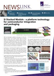
Packaging with Si carrier & <strong>TSV</strong><br />
(Source : Eric Beyne, IMEC)<br />
Source: IME’s Si stacked module (2005)<br />
(Ref : Knickerbocker, IBM J. Res & Dev, 2005)<br />
(Source : Intel, US)<br />
Silicon carrier with <strong>TSV</strong> is emerging solution <strong>for</strong> high per<strong>for</strong>mance integration plat<strong>for</strong>m
High Density Packaging Trend – <strong>TSV</strong> <strong>chip</strong> carrier<br />
Advantages<br />
• High density interconnect<br />
– Huge gap between front end<br />
scaling, interconnect pitch &<br />
substrate scaling<br />
• Absence of thermal mismatch, so<br />
micro-flip <strong>chip</strong> interconnection<br />
• Good thermal conductivity<br />
• Thin film process <strong>for</strong> embedded<br />
passives<br />
EPRC 9<br />
(Source : IBM)<br />
EPRC 7 & 8<br />
Ref: IME’s FCBGA and Stack <strong>chip</strong> module developed in EPRC 7 & 8<br />
• Silicon carrier can realize many advantages using its well established design & process technologies<br />
• IME has developed <strong>TSV</strong> related technologies since 2005
Proposed Project:<br />
<strong>TSV</strong> Technology <strong>for</strong> Packaging of <strong>Cu</strong> Low K Chip<br />
Objective:<br />
To develop <strong>TSV</strong> <strong>technology</strong> <strong>for</strong> <strong>Cu</strong>/Low K <strong>chip</strong> with very fine pitch<br />
interconnection involving:<br />
• Electrical design of Si interposer and a simplified organic substrate aiming<br />
<strong>for</strong> <strong>Cu</strong>/Ultra Low K <strong>chip</strong> application<br />
• Evaluation of <strong>TSV</strong> <strong>technology</strong> and develop processes <strong>for</strong> the Si interposer<br />
• Physical design, fabrication, assembly and reliability assessment<br />
Scope:<br />
• Electrical design and characterization of <strong>TSV</strong> interposer <strong>for</strong> FCBGA<br />
application<br />
• Mechanical design, modeling and optimization<br />
• <strong>TSV</strong> interposer process evaluation and fabrication<br />
• Assembly process evaluation, including fine pitch interconnection, under<br />
fill / flux material characterization and selection, wafer backgrind and dicing<br />
• Reliability assessment and failure analysis
Proposed Test Vehicle (Option 1)<br />
<strong>Cu</strong>/Low-K Large <strong>die</strong><br />
Si interposer with <strong>TSV</strong><br />
RoHS compliant<br />
Solder interconnect<br />
BT Substrate<br />
Features:<br />
Die size:<br />
>= 20x20mm*<br />
Chip <strong>technology</strong>: <strong>Cu</strong>/<strong>low</strong> K*<br />
<strong>Cu</strong> <strong>low</strong> K bump pitch: 150 um*<br />
Micro bump type<br />
solder<br />
<strong>TSV</strong> interposer bump pitch:
Proposed Test Vehicle (Option 2)<br />
Fine pitch Test <strong>chip</strong><br />
Si interposer with <strong>TSV</strong><br />
RoHS compliant<br />
Solder interconnect<br />
BT Substrate<br />
Features:<br />
Die size:<br />
>= 2x10x12mm*<br />
Chip <strong>technology</strong>:<br />
<strong>Cu</strong>/<strong>low</strong> K* or Al Test <strong>chip</strong><br />
Bump pitch:<br />
50, 100, 150 um<br />
Micro bump type<br />
solder, <strong>Cu</strong>, Au<br />
<strong>TSV</strong> interposer bump pitch:
Key Challenges<br />
• Packaging design<br />
– Electrical design & characterization <strong>for</strong> Si interposer<br />
• High speed interconnect / via design<br />
• Power distribution network design and optimization<br />
– Structural design and optimization<br />
• Stress analysis of detailed <strong>low</strong> K / ultra <strong>low</strong> K / Si<br />
interposer structures under assembly and reliability<br />
condition<br />
• Package / Si interposer design optimization<br />
• <strong>TSV</strong> interposer <strong>technology</strong><br />
– Dielectric isolation process<br />
– High speed via architectures<br />
– Via filling method<br />
– Thin wafer support<br />
• Assembly, materials, and reliability<br />
– Underfill, flux material selection<br />
– Wafer backgrinding and dicing (<strong>Cu</strong> <strong>low</strong> k bumped wafer &<br />
Silicon carrier)<br />
– Micro-bump interconnection and assembly processes<br />
– Reliability and FA
Project Deliverables<br />
• Design guidelines of using Si interposer with simplified organic<br />
substrate <strong>for</strong> FCBGA application<br />
• Electrical modeling results and characterization data <strong>for</strong> Si<br />
interposer with <strong>TSV</strong><br />
• Mechanical & thermal modeling results and optimization<br />
• Process details of Si interposer with <strong>TSV</strong><br />
• Micro-bump interconnection assembly characterization<br />
• Large <strong>die</strong> <strong>Cu</strong> <strong>low</strong> K assembly processes, including under fill, flux<br />
characterization and selection<br />
• Reliability assessment results and failure analysis