Diffraction Grating Effect on Waveguided Germanium MSM ...
Diffraction Grating Effect on Waveguided Germanium MSM ...
Diffraction Grating Effect on Waveguided Germanium MSM ...

Create successful ePaper yourself
Turn your PDF publications into a flip-book with our unique Google optimized e-Paper software.
R&D News<br />
<str<strong>on</strong>g>Diffracti<strong>on</strong></str<strong>on</strong>g> <str<strong>on</strong>g>Grating</str<strong>on</strong>g> <str<strong>on</strong>g>Effect</str<strong>on</strong>g> <strong>on</strong> <strong>Waveguided</strong><br />
<strong>Germanium</strong> <strong>MSM</strong> Photodetector Resp<strong>on</strong>se<br />
Dr. Ren Fang-Fang<br />
Senior Research Engineer, Nano-<br />
Electr<strong>on</strong>ics and Phot<strong>on</strong>ics Programme<br />
Dr. Ang Kah-Wee<br />
Senior Research Engineer, Nano-<br />
Electr<strong>on</strong>ics and Phot<strong>on</strong>ics Programme<br />
Dr. Patrick Lo G. Q.<br />
Program Director, Nano-Electr<strong>on</strong>ics<br />
and Phot<strong>on</strong>ics Programme<br />
<strong>Germanium</strong>-<strong>on</strong>-silic<strong>on</strong>-<strong>on</strong>-insulator<br />
(Ge-<strong>on</strong>-SOI) photodetectors<br />
have been actively pursued for<br />
optical interc<strong>on</strong>necti<strong>on</strong>/communicati<strong>on</strong><br />
applicati<strong>on</strong>s because of its large<br />
absorpti<strong>on</strong> coefficient [1] and its<br />
integrati<strong>on</strong> compatibility with silic<strong>on</strong><br />
(Si) complementary metal-oxidesemic<strong>on</strong>ductor<br />
(CMOS) process<br />
technology. In particular, the metalsemic<strong>on</strong>ductor-metal<br />
(<strong>MSM</strong>) c<strong>on</strong>figured<br />
photodiodes have been widely used due<br />
to its relative ease of fabricati<strong>on</strong> and high<br />
speed performance [2,3]. Although the<br />
<strong>MSM</strong> c<strong>on</strong>figured detector may exhibit<br />
low quantum efficiency and large dark<br />
current as compared to the p-i-n detector,<br />
the latter can be successfully overcome<br />
by incorporating a Si:C Schottky-barrier<br />
enhancement layer [4] or by using sulfursegregati<strong>on</strong><br />
at the NiGe/Ge interface<br />
to de-pin the Fermi level away from<br />
the valence band edge [5]. However,<br />
the illuminati<strong>on</strong> incident into the <strong>MSM</strong><br />
photodetectors may be sensitive to<br />
the dimensi<strong>on</strong> of interdigitated metallic<br />
electrodes that acts as a <strong>on</strong>e-dimensi<strong>on</strong><br />
diffracti<strong>on</strong> grating.<br />
The interdigitated structure acted as the<br />
metallic electrodes and a <strong>on</strong>e-dimensi<strong>on</strong>al<br />
(1D) metallic rectangular grating above the<br />
Ge active regi<strong>on</strong>. The measurements were<br />
operated at near-infrared wavelength of<br />
1.55 µm under transverse magnetic (TM)<br />
mode, because TM mode is more sensitive<br />
to diffracti<strong>on</strong> grating than transverse<br />
electric (TE) mode [6]. A relatively low<br />
dark current was observed due to an<br />
effective hole barrier modulati<strong>on</strong> by the<br />
Si:C Schottky barrier layer. Based <strong>on</strong> the<br />
optical near-field simulati<strong>on</strong>, we analyzed<br />
the relati<strong>on</strong>ship between photocurrent<br />
and optical energy c<strong>on</strong>fined inside the<br />
Ge regi<strong>on</strong>, dem<strong>on</strong>strating the diffracti<strong>on</strong><br />
effect induced by the metallic grating.<br />
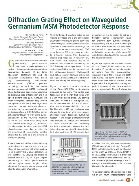
Figure 1 shows a schematic structure<br />
of the Ge-<strong>on</strong>-SOI <strong>MSM</strong> photodetector<br />
proposed in this work. The device was<br />
fabricated <strong>on</strong> an 8-inch SOI wafer with<br />
a 2 µm thick buried oxide. Dry etching<br />
was used to form a Si waveguide 220<br />
nm in thickness and 500 nm in width.<br />
After active window definiti<strong>on</strong>, a pure<br />
Ge film with ~500 nm thickness was<br />
allowed to grow in an ultra-high vacuum<br />
chemical vapor depositi<strong>on</strong> (UHVCVD)<br />
reactor. A thin silic<strong>on</strong>-germanium buffer<br />
was adopted to reduce the formati<strong>on</strong><br />
of misfit dislocati<strong>on</strong>s by minimizing<br />
the lattice mismatch between the two<br />
heterostructure materials [4]. A crystalline<br />
Si:C interfacial layer of ~20 nm was then<br />
deposited <strong>on</strong> the Ge regi<strong>on</strong> to act as a<br />
Schottky barrier enhancement layer<br />
for effective dark current reducti<strong>on</strong>.<br />
Subsequently, the SiO 2<br />
passivati<strong>on</strong> layer<br />
of 400nm was deposited and selectively<br />
dry etched to form c<strong>on</strong>tact hole. The<br />
metallizati<strong>on</strong> comprising of aluminum (Al)<br />
was deposited and patterned to complete<br />
the device fabricati<strong>on</strong>.<br />
Figure 1(a) depicts the top-view scheme<br />
of the interdigitated electrodes that<br />
formed a 1D metallic rectangular grating<br />
as shown from the cross-secti<strong>on</strong>al<br />
viewpoint [Figure 1(b)]. The groove depth<br />
was having the same thickness of Al<br />
layer, which was fixed at 400 nm in this<br />
experiment. The finger width, spacing and<br />
periodicity were indicated by w, s, and Λ=<br />
w + s, respectively. Figure 2 shows the<br />
Figure 2: Top-view SEM image of the Ge-<strong>on</strong>-<br />
SOI <strong>MSM</strong> photodetector featuring interdigitated<br />
electrodes with an effective device width W of 25<br />
µm and length L of 50 µm.<br />
To date, there are <strong>on</strong>ly few studies focusing<br />
<strong>on</strong> this issue and our aim is to study the<br />
effect of the electrode diffracti<strong>on</strong> grating<br />
in Ge Schottky <strong>MSM</strong> photodetectors <strong>on</strong><br />
SOI substrate by varying the electrode<br />
periods from 1.7, 1.8, to 1.9 µm. Higher<br />
resp<strong>on</strong>sivity in <strong>MSM</strong> photodetectors<br />
indicate higher noise margin, wider<br />
allowance for smaller device design and<br />
also the eliminati<strong>on</strong> of amplifier.<br />
Figure 1: Schematic illustrati<strong>on</strong> of the Ge-<strong>on</strong>-<br />
SOI <strong>MSM</strong> photodetector with interdigitated<br />
metal electrodes. (a) Top view of the<br />
interdigitated fingers. (b) Cross-secti<strong>on</strong>al view<br />
of the device structure.<br />
top-view scanning electr<strong>on</strong> microscopy<br />
(SEM) image of our fabricated Ge-<strong>on</strong>-SOI<br />
<strong>MSM</strong> detector structure with an effective<br />
device width W of 25 μm and a length L<br />
of 50 μm, respectively. Due to a difference<br />
in the refractive index between Si and Ge,<br />
the incidence phot<strong>on</strong> traveling in the Si<br />
waveguide would be up-coupled into the<br />
Ge regi<strong>on</strong> for absorpti<strong>on</strong>.<br />
The photoresp<strong>on</strong>se characteristics of the<br />
Ge-<strong>on</strong>-SOI <strong>MSM</strong> photodetectors were<br />
www.ime.a-star.edu.sg<br />
microE Bulletin | Issue 3 October 2009 11
R&D News<br />
By comparing Figure 5(a) with 5(b), the<br />
measured photocurrent showed good<br />
c<strong>on</strong>sistency with the simulated optical<br />
energy. The extent of c<strong>on</strong>finement<br />
and res<strong>on</strong>ant quality factor due to the<br />
diffracti<strong>on</strong> effect was shown to exhibit<br />
str<strong>on</strong>g dependence <strong>on</strong> the finger width<br />
geometry, which in turn resulted in a<br />
difference in the phot<strong>on</strong> absorpti<strong>on</strong>. During<br />
the process of simulati<strong>on</strong>, we assumed<br />
there were no optical absorpti<strong>on</strong> by the<br />
Ge layer so that we could estimate the<br />
optical energy inside the active regi<strong>on</strong>.<br />
Figure 3: Photoresp<strong>on</strong>se characteristics of a Ge-<strong>on</strong>-SOI interdigitated <strong>MSM</strong> photodetector with finger<br />
width w of 1.2 μm and spacing s of 0.6 μm. The optical measurement was performed by injecting a<br />
TM-mode incident electromagnetic (EM) wave with a wavelength λ of 1.55 μm into the Si waveguide<br />
and coupled into the Ge active regi<strong>on</strong> for absorpti<strong>on</strong>. The resp<strong>on</strong>sivity of the detector was calculated by<br />
subtracting the waveguide transmissi<strong>on</strong> loss of ~3.5 dB/cm and a coupling loss of ~4.5 dB.<br />
plotted in Figure 3. The devices were<br />
featuring w of 1.2 μm and s of 0.6 μm. At<br />
an applied bias of 1.0 V, a low dark current<br />
of 0.5 μA (0.4 nA/μm²) was measured.<br />
This measurement was below the typical<br />
1.0 µA generally c<strong>on</strong>sidered to be the<br />
upper limit for high speed receiver design<br />
and c<strong>on</strong>sistent with the previous reported<br />
value <strong>on</strong> <strong>MSM</strong> devices [3]. The optical<br />
measurement was performed by injecting<br />
a TM mode incident electromagnetic<br />
(EM) wave with a wavelength λ of 1.55<br />
µm into the Si waveguide and coupled<br />
into Ge active regi<strong>on</strong> for absorpti<strong>on</strong>. The<br />
incidence light power was estimated<br />
to be ~1 mW. At an applied bias of 1 V,<br />
the photocurrent was measured to be<br />
~1.51 mA. The resp<strong>on</strong>sivities were well<br />
dem<strong>on</strong>strated to be over 1 A/W.<br />
Figure 4: The normalized distributi<strong>on</strong> of magnetic<br />
field under TM mode in a photodetector with finger<br />
width w of 1.2 µm and spacing s of 0.6 µm.<br />
12 Institute of Microelectr<strong>on</strong>ics<br />
In order to evaluate the effect of the<br />
electrode diffracti<strong>on</strong> grating <strong>on</strong> the<br />
resp<strong>on</strong>se performance, the spatial<br />
distributi<strong>on</strong> of the magnetic field in the<br />
structure based <strong>on</strong> the Finite-Difference<br />
Time-Domain method was calculated as<br />
shown in Figure 4, for a detector with a<br />
w of 1.2 μm and s of 0.6 μm. It was noted<br />
that the optical field appeared to be locally<br />
c<strong>on</strong>centrated beneath the electrodes<br />
attributed to the diffracti<strong>on</strong> grating effect<br />
of metallic electrodes.<br />
To further c<strong>on</strong>firm the impact of the<br />
metallic grating, we compared the<br />
measurement and simulati<strong>on</strong> results<br />
for samples with varied electrode width<br />
w of 1.2, 1.3, and 1.4 µm (period Λ<br />
corresp<strong>on</strong>ding to 1.7, 1.8, and 1.9 µm)<br />
under TM modes, as shown in Figure 5(a)<br />
and 5(b). The spacing width s was fixed<br />
at 0.5 μm to maintain the same lateral<br />
spacing between the two adjacent fingers.<br />
The other structural parameters such as l<br />
and g (refer to Figure 1) were designed<br />
to ensure the same order dark current<br />
density. Photocurrent measurements<br />
were performed at an applied bias of<br />
1 V. In Figure 5(b), we integrated the<br />
optical energy localized in the whole Ge<br />
active layer for these three dimensi<strong>on</strong>s.<br />
Figure 5: <str<strong>on</strong>g>Effect</str<strong>on</strong>g>s of the electrode diffracti<strong>on</strong><br />
grating <strong>on</strong> the detector’s photoresp<strong>on</strong>se. (a) is the<br />
photocurrent measurement results at an applied<br />
bias of 1 V. (b) shows the calculated optical energy<br />
c<strong>on</strong>finement within the Ge regi<strong>on</strong>.<br />
In summary, Schottky interdigitated<br />
Ge-<strong>on</strong>-SOI <strong>MSM</strong> photodetectors with<br />
various finger width were fabricated<br />
with low dark current leakage. The<br />
photoresp<strong>on</strong>se exhibited str<strong>on</strong>g<br />
dependence <strong>on</strong> the finger width geometry,<br />
and showed good c<strong>on</strong>sistency with<br />
the numerical simulati<strong>on</strong>. The results<br />
imply that the occurrence of optical<br />
energy localizati<strong>on</strong> beneath the metallic<br />
electrodes is beneficial to achieve<br />
higher photoresp<strong>on</strong>se, which allows<br />
simultaneous achievement of high-speed<br />
resp<strong>on</strong>se and sufficient resp<strong>on</strong>sivity in a<br />
small semic<strong>on</strong>ductor element.<br />
References<br />
[1]<br />
[2]<br />
[3]<br />
[4]<br />
[5]<br />
[6]<br />
R. A. Soref, Proc. IEEE, 81(12), 1687<br />
(1993).<br />
J. Oh, S. Csutak, and J. C. Campbell, IEEE<br />
Phot<strong>on</strong>. Technol. Lett., 14, 369 (2002).<br />
K. W. Ang, S. Zhu, M. Yu, G. Q. Lo, and<br />
D. L. Kw<strong>on</strong>g, IEEE Phot<strong>on</strong>. Technol. Lett.,<br />
20(9), 754 (2008).<br />
K. W. Ang, S. Y. Zhu, J. Wang, K. T. Chua,<br />
M. B. Yu, G. Q. Lo, and D. L. Kw<strong>on</strong>g, IEEE<br />
Elect. Dev. Lett., 29(7), 704 (2008).<br />
K. W. Ang, M. B. Yu, S.Y. Zhu, K. T. Chua,<br />
G. Q. Lo, and D. L. Kw<strong>on</strong>g, IEEE Elect.<br />
Dev. Lett., 29(7), 708 (2008).<br />
A. S. Vengurlekar, Optics Lett., 33, 1669<br />
(2008).