Multiple-Chip Embedded Wafer Level Packaging
Multiple-Chip Embedded Wafer Level Packaging
Multiple-Chip Embedded Wafer Level Packaging

You also want an ePaper? Increase the reach of your titles
YUMPU automatically turns print PDFs into web optimized ePapers that Google loves.
IME Proprietary<br />
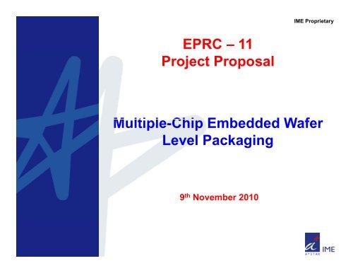
EPRC – 11<br />
Project Proposal<br />
<strong>Multiple</strong>-<strong>Chip</strong> l <strong>Embedded</strong> d <strong>Wafer</strong><br />
<strong>Level</strong> <strong>Packaging</strong><br />
9 th November 2010<br />
Slide 1
Motivation<br />
• High density packaging solution needed for mobile product<br />
→ Driver is Foot print, Thickness<br />
Ref: <strong>Chip</strong>works<br />
IME Proprietary<br />
“ Die / Board area ratio is 98 %<br />
Die/Package ratio is 160%. Packing<br />
density on the main board is the<br />
highest we’ve ever seen”.<br />
(Ref: <strong>Packaging</strong> for Portables; Going Vertical &<br />
Getting Small, David Carey)<br />
iPhone 4 main board : Component<br />
packing density<br />
Devices are today<br />
packaged in WLP<br />
Ref: Yole<br />
Slide 2<br />
Smart Phone IC <strong>Packaging</strong><br />
Ref: Global Semiconductor alliance
Technology Trend<br />
• Fan-out wafer level packaging: replacement of high pin-counts Pkg.<br />
→ Better electrical performance<br />
IME Proprietary<br />
Electrical parasitic fcBGA<br />
and eWLB @ 1GHz.<br />
Ref : Yole Development , 2010, <strong>Embedded</strong> <strong>Wafer</strong>-<strong>Level</strong>-<br />
Packages Fan-out WLP / <strong>Embedded</strong> die in PCB<br />
Ref : Seung Wook Yoon et al Thermal and<br />
Electrical l Characterization ti of eWLB<br />
(embedded <strong>Wafer</strong> <strong>Level</strong> BGA), ECTC2010<br />
Slide 3
Challenges to be addressed<br />
IME Proprietary<br />
Challenge<br />
12” wafer re-construction Die shift<br />
• .Material selection<br />
• Process control<br />
• Process modeling & prediction<br />
• Tape & mold material characterization<br />
Thin wafer handling<br />
• Warpage correction<br />
• Support wafer<br />
Approach<br />
Through Mold Connection<br />
• Wall smoothening<br />
• Electro-less less copper seed<br />
Printed Circuit Board<br />
Solder joint reliability<br />
<strong>Multiple</strong> layer RDL stress<br />
Power integrity<br />
• Stress isolation<br />
• Solder joint strengthening<br />
• Low temperature cure dielectric<br />
• Low stress material<br />
• De-coupling approach<br />
• <strong>Embedded</strong> / SMD passive<br />
Die 1 Die 2 Die 1 Die 2 Die 3<br />
Printed Circuit Board<br />
Printed Circuit Board<br />
Slide 4<br />
TV1 TV 2
Project Proposal<br />
IME Proprietary<br />
Objective: To develop embedded wafer packaging with multiple chip<br />
and discrete passive components involving<br />
• <strong>Wafer</strong> molding process modeling<br />
• 12” wafer re-construction process<br />
• Signal/power integrity it design<br />
• <strong>Multiple</strong> RDL Layer process<br />
• Through mold interconnection method<br />
• Solder joint reliability improvement<br />
Die 1 Die 2<br />
Die 1 Die 2 Die 3<br />
Printed Circuit Board<br />
TV 1 *:<br />
• Package size < 10mm<br />
• 2 chip with discrete passive<br />
• 2 RDL Layers<br />
Printed Circuit Board<br />
TV 2 *:<br />
• Package size > 10mm<br />
• 3 chip with discrete passive<br />
• 3 RDL layers<br />
Slide 5<br />
* To be finalized with members input
<strong>Wafer</strong> Molding Analysis<br />
IME Proprietary<br />
• Re-construction process modeling<br />
o Material characterization for<br />
modeling<br />
• Viscosity<br />
• Gel temperature<br />
• Mechanical properties<br />
o Cure kinetics<br />
• Degree of cure<br />
o Molding process simulation<br />
• Temperature, time, pressure<br />
Cure Cycle<br />
•Effect t of packaging density<br />
o Die layout<br />
o Die thickness<br />
o Number of die<br />
o Mold thickness<br />
Slide 6<br />
•Model validation<br />
o Warpage measurement<br />
o Die shift measurement<br />
Degree of Cure<br />
Ref: Min Woo Lee, Rheological Characterization and Full 3D<br />
Mold Flow Simulation in Multi-Die Stack CSP of <strong>Chip</strong> Array<br />
<strong>Packaging</strong>, ECTC2006
<strong>Wafer</strong> Re-construction<br />
• 300mm wafer level molding<br />
process<br />
o Evaluation of molding material<br />
• Liquid , Granular<br />
o Process condition<br />
• Temperature, time, pressure<br />
o Post mold treatment<br />
• Die shift analysis & control<br />
o Evaluation of re-configuration tape<br />
• Adhesion, temperature stability<br />
o Die pick & place tolerance<br />
o Mold material & Process<br />
o Minimum clearance between die<br />
• <strong>Wafer</strong> warpage control<br />
o Thermal treatment<br />
o Support system<br />
o Mold material<br />
Slide 7<br />
Mold process temperaturet<br />
IME Proprietary<br />
Ref: IME<br />
Die shift analysis<br />
Large Warpage<br />
Ref: IME<br />
Ref: IME
Re-distribution & Interconnection<br />
IME Proprietary<br />
• Re-distribution<br />
o <strong>Multiple</strong> layers of re-distribution metal<br />
layers<br />
• Sputtered seed, electro-less seed<br />
o Low temperate cure & low stress dielectric<br />
o Dielectric material adhesion on molded<br />
wafer<br />
o Cu seed adhesion on the mold material<br />
• Through Mold Interconnection<br />
o Via formation<br />
• Wall roughness conditioning<br />
o Electroplated /Electroless – Cu<br />
o Via filling methods<br />
<strong>Multiple</strong> layer<br />
RDL<br />
Ref: IME<br />
Through mold<br />
connection<br />
Slide 8
Electrical Design<br />
• Freq domain analysis / testing<br />
o Upto 20 GHz<br />
o TL from PCB to DIE<br />
• CPW and MSL benchmarking<br />
o <strong>Chip</strong> to chip connection (RDL)<br />
• Power Decoupling Networks (PDN) analysis / testing<br />
o DeCap location<br />
• Signal & Power integrity analysis<br />
o C2C interconnection ( Side by Side)<br />
• Electrical characterization of mold compound &<br />
Through mold connection<br />
o Dk, tanθ up to 10 GHz<br />
IME Proprietary<br />
Mold<br />
DeCap<br />
RD<br />
L<br />
IC#1<br />
IC#2<br />
PCB<br />
Slide 9
Package Reliability<br />
IME Proprietary<br />
• Solder joint reliability<br />
o Interconnect structure design and stress<br />
analysis<br />
o UBM, Pad finish<br />
o Stress isolation<br />
o Solder joint strengthening<br />
• Package reliability assessment<br />
o TCOB<br />
o MSL<br />
o HAST<br />
o Drop test<br />
• Failure Analysis<br />
o Mold void<br />
o Die stress<br />
o Dielectric delamination<br />
o Solder joint failure<br />
Slide 10
Project Flow<br />
IME Proprietary<br />
Members Input<br />
Test Vehicle definition<br />
<strong>Wafer</strong> – Reconstruction<br />
& Molding<br />
Mold and tape selection &<br />
characterization<br />
Compression molding<br />
process modeling<br />
<strong>Wafer</strong> re-construction<br />
experiments and die shift<br />
analysis<br />
Design & Analysis<br />
Signal & Power integrity<br />
it<br />
analysis<br />
Characterization of<br />
Through mold connection<br />
Package stress analysis<br />
and solder joint reliability<br />
improvements<br />
<strong>Wafer</strong> level & assembly<br />
Process<br />
Double side RDL, Dielectric<br />
material selection<br />
Warpage correction study<br />
Through- mold<br />
interconnection method<br />
Package assembly Process<br />
Project Time line and<br />
schedule :<br />
Feb 2011 to Aug 2012<br />
Slide 11<br />
Test Vehicles<br />
Fabrication & assembly<br />
Reliability Testing &<br />
Failure analysis
Research Outcome<br />
IME Proprietary<br />
• Design<br />
o Signal integrity analysis results and design guide line<br />
o Power integrity design and analysis results<br />
o Modeling approach for wafer re-construction process and die shift<br />
control guide line<br />
o Large package thermo-mechanical reliability improvement method<br />
•Process<br />
o 12” wafer re-construction process details and mold material<br />
characterization<br />
o <strong>Wafer</strong> warpage data and reduction methods<br />
o Dielectric material evaluation and adhesion characterization<br />
o <strong>Multiple</strong> layer RDL process details<br />
o Through mold interconnection method<br />
• Package assembly<br />
o Package age assembly process details<br />
•Package reliability evaluation<br />
o Package reliability evaluation results, failure identification and root<br />
cause analysis<br />
Slide 12
IME Proprietary<br />
Thanks for your attention<br />
Slide 13