Download Datasheet - Infineon
Download Datasheet - Infineon
Download Datasheet - Infineon

You also want an ePaper? Increase the reach of your titles
YUMPU automatically turns print PDFs into web optimized ePapers that Google loves.
EiceDRIVER TM<br />
2ED300C17-S/-ST<br />
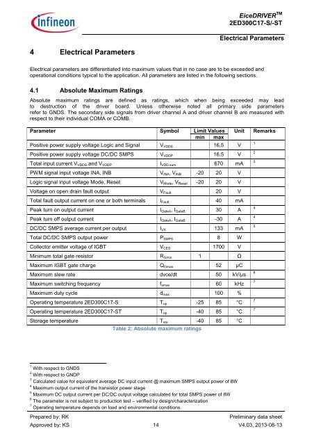
Electrical Parameters<br />
4 Electrical Parameters<br />
Electrical parameters are differentiated into maximum values that in no case are to be exceeded and<br />
operational conditions typical to the application. All parameters are listed in the following sections.<br />
4.1 Absolute Maximum Ratings<br />
Absolute maximum ratings are defined as ratings, which when being exceeded may lead<br />
to destruction of the driver board. Unless otherwise noted all primary side parameters<br />
refer to GNDS. The secondary side signals from driver channel A and driver channel B are measured with<br />
respect to their individual COMA or COMB.<br />
Parameter Symbol Limit Values Unit Remarks<br />
min max<br />
Positive power supply voltage Logic and Signal V VDDS 16,5 V<br />
Positive power supply voltage DC/DC SMPS V VDDP 16,5 V<br />
Total input current V VDDS and V VDDP I VDD,sum 670 mA<br />
PWM signal input voltage INA, INB V INA , V INB -20 20 V<br />
Logic signal input voltage Mode, Reset V Mode , V Reset -20 20 V<br />
Voltage on open drain fault output V Fault 20 V<br />
Total fault output current on one or both terminals I Fault 40 mA<br />
Peak turn on output current I GateA , I GateB 30 A<br />
Peak turn off output current I GateA , I GateB -30 A<br />
DC/DC SMPS average current per output I VX 133 mA<br />
Total DC/DC SMPS output power P SMPS 8 W<br />
Collector emitter voltage of IGBT V CES 1700 V<br />
Minimum total gate resistor R Gmin 1 Ω<br />
Maximum IGBT gate charge Q Gmax 52 µC<br />
Maximum slew rate dvce/dt 50 kV/µs<br />
Maximum switching frequency f smax 60 kHz<br />
Maximum duty cycle d max 100 %<br />
Operating temperature 2ED300C17-S T op -25 85 °C<br />
Operating temperature 2ED300C17-ST T op -40 85 °C<br />
Storage temperature T sto -40 85 °C<br />
Table 2: Absolute maximum ratings<br />
1<br />
2<br />
3<br />
4<br />
4<br />
5<br />
6<br />
7<br />
7<br />
7<br />
1 With respect to GNDS<br />
2 With respect to GNDP<br />
3 Calculated value for equivalent average DC input current @ maximum SMPS output power of 8W<br />
4 Maximum output current of the transistor power stage<br />
5 Maximum DC output current per DC/DC output voltage calculated for total SMPS power of 8W<br />
6 The parameter is not subject to production test – verified by design/characterization<br />
7 Operating temperature depends on load and environmental conditions.<br />
Prepared by: RK<br />
Preliminary data sheet<br />
Approved by: KS 14 V4.03, 2013-08-13