Download Datasheet - Infineon
Download Datasheet - Infineon
Download Datasheet - Infineon

You also want an ePaper? Increase the reach of your titles
YUMPU automatically turns print PDFs into web optimized ePapers that Google loves.
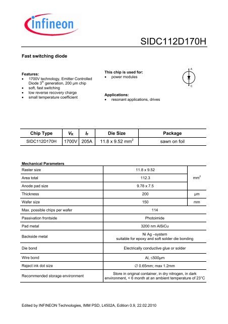
SIDC112D170H<br />
Fast switching diode<br />
Features:<br />
• 1700V technology, Emitter Controlled<br />
Diode 3 th generation, 200 µm chip<br />
• soft, fast switching<br />
• low reverse recovery charge<br />
• small temperature coefficient<br />
This chip is used for:<br />
• power modules<br />
Applications:<br />
• resonant applications, drives<br />
A<br />
C<br />
Chip Type V R I F Die Size Package<br />
SIDC112D170H 1700V 205A 11.8 x 9.52 mm 2 sawn on foil<br />
Mechanical Parameters<br />
Raster size 11.8 x 9.52<br />
Area total 112.3<br />
mm 2<br />
Anode pad size 9.78 x 7.5<br />
Thickness 200 µm<br />
Wafer size 150 mm<br />
Max. possible chips per wafer 114<br />
Passivation frontside<br />
Pad metal<br />
Backside metal<br />
Die bond<br />
Wire bond<br />
Reject ink dot size<br />
Recommended storage environment<br />
Photoimide<br />
3200 nm AlSiCu<br />
Ni Ag –system<br />
suitable for epoxy and soft solder die bonding<br />
Electrically conductive glue or solder<br />
Al, ≤500µm<br />
∅ 0.65mm; max 1.2mm<br />
Store in original container, in dry nitrogen, in dark<br />
environment, < 6 month at an ambient temperature of 23°C<br />
Edited by INFINEON Technologies, IMM PSD, L4502A, Edition 0.9, 22.02.2010
SIDC112D170H<br />
Maximum Ratings<br />
Parameter Symbol Condition Value Unit<br />
Repetitive peak reverse voltage V RRM T vj = 25 °C 1700 V<br />
Continuous forward current I F T vj < 150°C<br />
Maximum repetitive forward current I FRM T vj < 150°C 410<br />
Junction temperature range T vj -40...+175 °C<br />
Operating junction temperature T vj -40...+150 °C<br />
Dynamic ruggedness² )<br />
P max<br />
1 ) depending on thermal properties of assembly<br />
2 ) not subject to production test - verified by design/characterisation<br />
I Fmax = 410A, V Rmax =<br />
1700V, T vj ≤ 150°C<br />
1 )<br />
tbd<br />
A<br />
kW<br />
Static Characteristic (tested on wafer), T vj = 25 °C<br />
Parameter Symbol Conditions<br />
Value<br />
min. typ. max.<br />
Reverse leakage current I R V R =1700V 20 µA<br />
Cathode-Anode<br />
breakdown Voltage<br />
3)<br />
Diode forward voltage V F<br />
3)<br />
V F tested at lower current<br />
V BR I R =0.25mA 1700 V<br />
Unit<br />
I F =205A 1.9 2.3 V<br />
Further Electrical Characteristics<br />
Switching characteristics and thermal properties are depending strongly on module design and mounting<br />
technology and can therefore not be specified for a bare die.<br />
Edited by INFINEON Technologies, IMM PSD, L4502A, Edition 0.9, 22.02.2010
SIDC112D170H<br />
Chip Drawing<br />
A<br />
A: Anode pad<br />
Edited by INFINEON Technologies, IMM PSD, L4502A, Edition 0.9, 22.02.2010
SIDC112D170H<br />
FURTHER ELECTRICAL CHARACTERISTICS<br />
This chip data sheet refers to the<br />
module data sheet<br />
DESCRIPTION<br />
AQL 0,65 for visual inspection according to failure catalogue<br />
Electrostatic Discharge Sensitive Device according to MIL-STD 883<br />
REVISION HISTORY<br />
Version Subjects (major changes since last revision) Date<br />
Published by<br />
<strong>Infineon</strong> Technologies AG<br />
81726 Munich, Germany<br />
© 2010 <strong>Infineon</strong> Technologies AG<br />
All Rights Reserved.<br />
Legal Disclaimer<br />
The information given in this document shall in no event be regarded as a guarantee of conditions or<br />
characteristics. With respect to any examples or hints given herein, any typical values stated herein and/or<br />
any information regarding the application of the device, <strong>Infineon</strong> Technologies hereby disclaims any and all<br />
warranties and liabilities of any kind, including without limitation, warranties of non-infringement of intellectual<br />
property rights of any third party.<br />
Information<br />
For further information on technology, delivery terms and conditions and prices, please contact the nearest<br />
<strong>Infineon</strong> Technologies Office (www.infineon.com).<br />
Warnings<br />
Due to technical requirements, components may contain dangerous substances. For information on the<br />
types in question, please contact the nearest <strong>Infineon</strong> Technologies Office. <strong>Infineon</strong> Technologies<br />
components may be used in life-support devices or systems only with the express written approval of<br />
<strong>Infineon</strong> Technologies, if a failure of such components can reasonably be expected to cause the failure of<br />
that life-support device or system or to affect the safety or effectiveness of that device or system. Life support<br />
devices or systems are intended to be implanted in the human body or to support and/or maintain and<br />
sustain and/or protect human life. If they fail, it is reasonable to assume that the health of the user or other<br />
persons may be endangered.<br />
Edited by INFINEON Technologies, IMM PSD, L4502A, Edition 0.9, 22.02.2010