Download Datasheet - Infineon
Download Datasheet - Infineon
Download Datasheet - Infineon
Create successful ePaper yourself
Turn your PDF publications into a flip-book with our unique Google optimized e-Paper software.
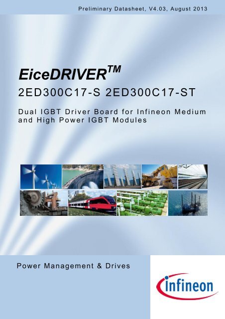
P r e l i minary <strong>Datasheet</strong> , V 4. 0 3, A u g u st 2013<br />
EiceDRIVER TM<br />
2ED300C17-S 2ED300C17-ST<br />
D u a l I G B T D r i v e r B o a r d f o r I n f i n e o n M e d i u m<br />
a n d H i g h P o w e r I G B T M o d u l e s<br />
Power Management & Drives
EiceDRIVER TM<br />
2ED300C17-S/-ST<br />
2ED300C17-S 2ED300C17-ST<br />
Revision History: 2013-08 V4.03<br />
Previous Version: V4.02<br />
Version Page Subjects (major changes since last revision)<br />
4.03 2 Revision history modified. All changes included.<br />
4.03 8; 18 Figure 4 and figure7 size changed.<br />
4.02 19 Partial discharge test voltage added<br />
4.02 Chapter 4.5 and 4.6 added<br />
4.01 Update figure 2 and figure 6<br />
4.00 all General review, new hardware version V6<br />
Edition 2013-08-13<br />
Published by<br />
<strong>Infineon</strong> Technologies AG<br />
59568 Warstein, Germany<br />
© <strong>Infineon</strong> Technologies AG 2013.<br />
All Rights Reserved.<br />
ATTENTION PLEASE!<br />
THE INFORMATION HEREIN IS GIVEN TO DESCRIBE CERTAIN COMPONENTS AND SHALL NOT BE<br />
CONSIDERED AS A GUARANTEE OF CHARACTERISTICS.<br />
TERMS OF DELIVERY AND RIGHTS TO TECHNICAL CHANGE RESERVED.<br />
WE HEREBY DISCLAIM ANY AND ALL WARRANTIES, INCLUDING BUT NOT LIMITED TO<br />
WARRANTIES OF NON-INFRINGEMENT, REGARDING CIRCUITS, DESCRIPTIONS AND CHARTS<br />
STATED HEREIN.<br />
Information<br />
For further information on technology, delivery terms and conditions and prices please contact your nearest<br />
<strong>Infineon</strong> Technologies Office (www.infineon.com).<br />
Warnings<br />
Due to technical requirements components may contain dangerous substances. For information on the types<br />
in question please contact your nearest <strong>Infineon</strong> Technologies Office.<br />
<strong>Infineon</strong> Technologies Components may only be used in life-support devices or systems with the express<br />
written approval of <strong>Infineon</strong> Technologies, if a failure of such components can reasonably be expected to<br />
cause the failure of that life-support device or system, or to affect the safety or effectiveness of that device or<br />
system. Life support devices or systems are intended to be implanted in the human body, or to support<br />
and/or maintain and sustain and/or protect human life. If they fail, it is reasonable to assume that the health<br />
of the user or other persons may be endangered.
EiceDRIVER TM<br />
2ED300C17-S/-ST<br />
Safety notice<br />
The driver may only be used for the purposes described by the manufacturer.<br />
Inadmissible alterations and use of spare parts or accessories not recommend by <strong>Infineon</strong><br />
may cause fire, electric shock and injuries.<br />
This document has to be available to all users, developers and qualified personnel working<br />
with the driver.<br />
If measurements and tests on the device have to be carried out during operation,<br />
the regulations of the work on live parts are to be observed and suitable test equipment<br />
is to be used.<br />
Prior to installation and commissioning please read this document thoroughly.<br />
Commissioning is prohibited if there is visible damage by inappropriate handling<br />
or transportation.<br />
Ensure ESD protection during handling.<br />
Connect or disconnect only when power is turned off.<br />
Always keep sufficient safety distance during commissioning without closed<br />
protective housing.<br />
Contact under live condition is strictly prohibited.<br />
Work after turn-off is impermissible until the absence of supply voltage has been<br />
verified.<br />
During work after turn-off it has to be observed that components heat up during<br />
operation. Contact can cause injuries.<br />
Electrically and mechanically, the driver is mounted onto customer’s PCB by<br />
soldering. The mechanical strength has to be verified by the user and, if necessary,<br />
assured with appropriate tests.<br />
The driver is designed to be used in combination with <strong>Infineon</strong> IGBT modules,<br />
especially IHM, EconoPACK+, PrimePACK TM and 62mm. In case of ulterior use,<br />
safe operation cannot be ensured.<br />
Exclusion clause:<br />
The datasheet is part of the <strong>Infineon</strong> IGBT driver 2ED300C17-S/-ST. To ensure safe and reliable operation<br />
it is necessary to read and understand this datasheet.<br />
The <strong>Infineon</strong> IGBT driver 2ED300C17-S/-ST is only intended for control of <strong>Infineon</strong> IGBT modules.<br />
<strong>Infineon</strong> cannot warrant against damage and/or malfunction if IGBT modules used not produced by <strong>Infineon</strong>.<br />
In this context, <strong>Infineon</strong> retains the right to change technical data and product specifications without prior<br />
notice to the course of improvement.<br />
Prepared by: RK<br />
Preliminary data sheet<br />
Approved by: KS 3 V4.03, 2013-08-13
EiceDRIVER TM<br />
2ED300C17-S/-ST<br />
This side is intentionally left blank.<br />
Prepared by: RK<br />
Preliminary data sheet<br />
Approved by: KS 4 V4.03, 2013-08-13
EiceDRIVER TM<br />
2ED300C17-S/-ST<br />
Dual channel high voltage IGBT driver board<br />
Product Highlights<br />
Galvanically isolated dual channel IGBT driver<br />
Reinforced isolation according to EN 50178<br />
Integrated protection features<br />
5kV isolation test performed as 100% test<br />
High Electromagnetic Compatibility<br />
Features<br />
<br />
<br />
<br />
<br />
<br />
<br />
<br />
<br />
<br />
<br />
<br />
<br />
<br />
<br />
Designed for <strong>Infineon</strong> IGBT modules up to 1700V<br />
High peak output current of 30A<br />
Integrated DC-DC SMPS<br />
Soft Shut Down in fault conditions<br />
Dynamic Over Current Detection<br />
IGBT desaturation monitoring<br />
Interlocking in half-bridge mode<br />
Open drain fault output<br />
Low impedance 15V inputs for high noise immunity<br />
±15 V secondary drive voltage<br />
Short propagation delay time<br />
Optional sense function<br />
RoHS compliant<br />
UL94V-2 compliant materials<br />
Typical Applications<br />
Renewable energies<br />
Drives and automation<br />
Transportation<br />
Power supplies<br />
Medical<br />
UPS systems<br />
Figure 1: Basic schematic for driver setup<br />
Prepared by: RK<br />
Preliminary data sheet<br />
Approved by: KS 5 V4.03, 2013-08-13
EiceDRIVER TM<br />
2ED300C17-S/-ST<br />
Table of Contents<br />
1 Block Diagram and Schematic..................................................................................................... 7<br />
2 Functional Description ................................................................................................................. 8<br />
2.1 Reinforced Isolation ........................................................................................................................ 8<br />
2.2 Integrated SMPS ............................................................................................................................. 9<br />
2.3 Undervoltage Lockout (UVLO) ........................................................................................................ 9<br />
2.4 Dynamic Overcurrent Detection (DOCD) ........................................................................................ 9<br />
2.5 Soft Shut Down (SSD) .................................................................................................................... 9<br />
2.6 External Detected Failure Analysis (EDFA) .................................................................................... 9<br />
2.7 Reset ............................................................................................................................................... 9<br />
2.8 Control Inputs and Outputs 2ED300C17-S /-ST ............................................................................. 9<br />
3 Pin Configuration and Functionality ......................................................................................... 10<br />
3.1 Pin functionalities, Primary side .................................................................................................... 11<br />
3.2 Pin functionalities, Secondary side ............................................................................................... 12<br />
4 Electrical Parameters .................................................................................................................. 14<br />
4.1 Absolute Maximum Ratings .......................................................................................................... 14<br />
4.2 Operating Parameters ................................................................................................................... 15<br />
4.3 Recommended Operating Parameters ......................................................................................... 15<br />
4.4 Electrical Characteristics ............................................................................................................... 16<br />
4.5 Driver performance ....................................................................................................................... 17<br />
4.6 VCESAT reference ........................................................................................................................ 18<br />
5 Isolation characteristics ............................................................................................................. 19<br />
6 Timing diagrams ......................................................................................................................... 20<br />
7 Mechanical dimensions .............................................................................................................. 21<br />
8 Handling and mounting .............................................................................................................. 23<br />
Page<br />
Prepared by: RK<br />
Preliminary data sheet<br />
Approved by: KS 6 V4.03, 2013-08-13
EiceDRIVER TM<br />
2ED300C17-S/-ST<br />
Block Diagram and Schematic<br />
1 Block Diagram and Schematic<br />
Figure 2: Block Diagram 2ED300C17-S/-ST<br />
Figure 3: Peripheric components for half-bridge mode<br />
Prepared by: RK<br />
Preliminary data sheet<br />
Approved by: KS 7 V4.03, 2013-08-13
EiceDRIVER TM<br />
2ED300C17-S/-ST<br />
Functional Description<br />
2 Functional Description<br />
EiceDRIVER (eupec IGBT controlled efficiency DRIVER) is the name of a family of IGBT-Drivers<br />
consisting of IGBT driver boards and IGBT driver ICs.<br />
The 2ED300C17-S/-ST is a dual channel high voltage gate driver board featuring reinforced isolation<br />
between logic side and high voltage output.<br />
Control and protection functions are included to ease the design of highly reliable systems.<br />
The 2ED300C17-S is designed for use in industrial applications and the 2ED300C17-ST, with special<br />
coating, for the use in more demanding applications like railway traction or windmills.<br />
The device consists of two galvanically separated driver channels and features two operating functions, the<br />
direct mode and the half-bridge mode, to drive IGBT modules.<br />
The 2ED300C17-S/-ST is designed for use with <strong>Infineon</strong> IGBT modules up to 1700V in applications with high<br />
safety and reliability requirements and aims for power ratings of 75kW to 1MW.<br />
The driver also includes IGBT desaturation protection, external failure input and Undervoltage Lockout<br />
(UVLO) detection. All fault states set the fault memory and activate the open drain fault output.<br />
2.1 Reinforced Isolation<br />
The most important safety feature of the 2ED300C17-S/-ST high voltage driver board is the reinforced<br />
isolation between primary and secondary side. This is achieved by using a specially designed transformer<br />
characterized by lowest coupling capacitances, , high isolation stability and by appropriate creepage and<br />
clearance distances on the printed circuit board. Figure 4 shows the specially transformer design for high<br />
isolation solution.<br />
The clearance and creepage distances comply with VDE0110 and VDE0160 / EN50178 and are designed<br />
for pollution degree 3, over voltage class III. All materials used within the transformer at least meet the<br />
requirements of UL94V-2.<br />
Figure 4: Additionally mechanical barriers for high isolation solution<br />
Prepared by: RK<br />
Preliminary data sheet<br />
Approved by: KS 8 V4.03, 2013-08-13
EiceDRIVER TM<br />
2ED300C17-S/-ST<br />
Functional Description<br />
2.2 Integrated SMPS<br />
A switch mode power supply with galvanically separated outputs is integrated on the 2ED300C17-S/-ST.<br />
It generates the required voltages for both driver channels. The secondary supplies are not protected against<br />
external short circuit.<br />
2.3 Undervoltage Lockout (UVLO)<br />
Undervoltage monitoring is implemented for both secondary sides, positive and negative driver supply<br />
voltages are monitored. The Signal and Logic side is not monitored. Undervoltage lockout functionality in<br />
both driver channels ensures correct IGBT switching operation.<br />
If the absolute value of one of the driver channel’s power supplies drops below the UVLO detection level, the<br />
IGBT is shut down using the soft shut down functionality; gate-signals are ignored and the fault output is<br />
activated.<br />
2.4 Dynamic Overcurrent Detection (DOCD)<br />
The dynamic over current detection protects the IGBT in case of a short circuit. The saturation voltage during<br />
IGBT on-state is measured and continuously compared with a defined reference signal.<br />
The shut down reference curve has to be adapted to each individual IGBT connecting an external RC<br />
network. If no measures are taken, the reference level for desaturation detection is approx. at 10 V. Adding<br />
an RC network allows to tune the characteristics of the detection circuit.<br />
2.5 Soft Shut Down (SSD)<br />
Soft shut down is a technique to limit the current slope di/dt during turn-off. It is activated if the fault memory<br />
is set as a consequence of a detected fault condition. A sense terminal can optionally be used to connect an<br />
additional external resistor. This is done to adjusting the IGBT turn-off characteristics. This terminal can<br />
optionally be used as an input for the active clamping or di/dt and dv/dt control.<br />
2.6 External Detected Failure Analysis (EDFA)<br />
Additional function, customizable according to individual applications such as thermo switches on heat sinks.<br />
Digital high level on these terminals set the fault memory. Soft shut down is initiated and further operation<br />
inhibited.<br />
2.7 Reset<br />
Resetting the driver can be done by applying a digital high level to the Reset-pin or by applying a digital low<br />
level to both gate-signal inputs for at least 60ms.On Reset, the fault memory is deleted and restarting driver<br />
operation is possible.<br />
2.8 Control Inputs and Outputs 2ED300C17-S /-ST<br />
Inputs of the Signal and Logic side require 15V CMOS levels according to 40xx CMOS technology. This<br />
offers a high signal to noise ratio. In very harsh environments, negative low level input signals can be used<br />
with the limits given for the maximum ratings.<br />
The open drain fault output is a very low impedance output. Voltage levels similar to Signal and Logic ground<br />
are achieved.<br />
Prepared by: RK<br />
Preliminary data sheet<br />
Approved by: KS 9 V4.03, 2013-08-13
3 Pin Configuration and Functionality<br />
EiceDRIVER TM<br />
2ED300C17-S/-ST<br />
Pin Configuration and Functionality<br />
Pin Label Function<br />
1<br />
2<br />
3<br />
4<br />
VDDS<br />
/Fault<br />
Signal and logic supply voltage primary side<br />
Open drain fault output<br />
5 Reset Active high signal and logic reset input<br />
6 CA External capacitor terminal for half-bridge mode dead time adjustment channel A<br />
7 INB Active high PWM input channel B<br />
8 CB External capacitor terminal for half-bridge mode dead time adjustment channel B<br />
9 Mode Operating mode selection input<br />
10 /Fault Open drain fault output<br />
11 INA Active high PWM input channel A<br />
12<br />
13<br />
GNDS Signal and logic common ground primary side<br />
14<br />
15<br />
16<br />
17<br />
18<br />
19<br />
20<br />
21<br />
22<br />
23<br />
24<br />
VDDP<br />
GNDP<br />
E.B<br />
DC/DC-SMPS supply voltage primary side<br />
DC/DC-SMPS ground primary side<br />
Active high external digital fault input driver channel B<br />
25 VCEsatB IGBT desaturation sensing input driver channel B<br />
26 RCB Desaturation reference curve RC network terminal driver channel B<br />
27 SenseB Active clamping input or soft shut down resistor terminal driver channel B<br />
28 VB- External capacitor terminal for negative power supply driver channel B<br />
29 VB+ External capacitor terminal for positive power supply driver channel B<br />
30<br />
31<br />
COMB Common ground terminal driver channel B<br />
32<br />
33<br />
GateB IGBT gate output driver channel B<br />
34 Pin not existing; cut out<br />
35 Pin not existing; cut out<br />
36 E.A Active high external digital fault input driver channel A<br />
37 VCEsatA IGBT desaturation sensing input driver channel A<br />
38 RCA Desaturation reference curve RC network terminal driver channel A<br />
39 SenseA Active clamping input or soft shut down resistor terminal driver channel A<br />
40 VA- External capacitor terminal for negative power supply driver channel A<br />
41 VA+ External capacitor terminal for positive power supply driver channel A<br />
42<br />
43<br />
COMA Common ground terminal driver channel A<br />
44<br />
45<br />
GateA IGBT gate output driver channel A<br />
Table 1 : Pin Configuration of 2ED300C17-S/-ST<br />
Prepared by: RK<br />
Preliminary data sheet<br />
Approved by: KS 10 V4.03, 2013-08-13
In addition to Table 1, Figure 5 gives an overview on the pin positions.<br />
EiceDRIVER TM<br />
2ED300C17-S/-ST<br />
Pin Configuration and Functionality<br />
Figure 5 : EiceDRIVER pinning top view<br />
3.1 Pin functionalities, Primary side<br />
All input pins are compatible to 15V CMOS logic according to 40xx technology.<br />
VDDS<br />
15V supply voltage for signal and logic part on the primary side. All pins have to be connected.<br />
/Fault<br />
Open drain fault output for signalization of internal and external faults. Reset signal required to delete the<br />
fault memory and for restarting operation after fault state.<br />
External pull-up resistor needed.<br />
Reset<br />
Active high signal to delete the fault memory.<br />
INA<br />
Active high signal for PWM, channel A. Negative input voltage for low level is allowed within the limits given<br />
for maximum values.<br />
INB<br />
Active high signal for PWM, channel B. Negative input voltage for low level is allowed within the limits given<br />
for maximum values.<br />
Prepared by: RK<br />
Preliminary data sheet<br />
Approved by: KS 11 V4.03, 2013-08-13
CA<br />
EiceDRIVER TM<br />
2ED300C17-S/-ST<br />
Pin Configuration and Functionality<br />
Terminal to connect external capacitor for dead time adjustment of channel A in half-bridge mode.<br />
CB<br />
Terminal to connect external capacitor for dead time adjustment of channel B in half-bridge mode.<br />
Mode<br />
Terminal for mode selection, choosing direct mode or half-bridge mode. High level or connection to VDDS<br />
activates half-bridge mode. Low level or connection to ground GNDS activates direct mode.<br />
GNDS<br />
Common ground connection for signals and supply voltage of Signal and Logic part.<br />
All pins have to be connected.<br />
Connection between GNDS and GNDP is permissible.<br />
VDDP<br />
15V supply voltage for DC/DC switch mode power supply. An external capacitor to GNDP is mandatory at<br />
this terminal.<br />
All pins have to be connected.<br />
GNDP<br />
Ground connection for DC/DC switch mode power supply.<br />
All pins have to be connected.<br />
Connection between GNDS and GNDP is permissible.<br />
3.2 Pin functionalities, Secondary side<br />
GateA<br />
Output to IGBT gate, driver channel A. Both pins have to be connected.<br />
COMA<br />
Common ground connection for IGBT auxiliary emitter and all signals of driver channel A. Both pins have to<br />
be connected.<br />
VA+<br />
Positive power supply, driver channel A. An external capacitor to ground COMA is mandatory at this<br />
terminal.<br />
VA-<br />
Negative power supply driver channel A. An external capacitor to ground COMA is mandatory at this<br />
terminal.<br />
Prepared by: RK<br />
Preliminary data sheet<br />
Approved by: KS 12 V4.03, 2013-08-13
SenseA<br />
EiceDRIVER TM<br />
2ED300C17-S/-ST<br />
Pin Configuration and Functionality<br />
Terminal for additional external soft shut down resistor or input for active clamping, di/dt or dv/dt control,<br />
driver channel A<br />
RCA<br />
Desaturation reference curve RC network terminal, driver channel A<br />
VCEsatA<br />
IGBT desaturation sensing input, driver channel A.<br />
E.A<br />
Active high external digital fault input driver channel A for set fault memory.<br />
GateB<br />
Output to IGBT gate, driver channel B. Both pins have to be connected.<br />
COMB<br />
Common ground connection for IGBT auxiliary emitter and all signals of driver channel B. Both pins have to<br />
be connected.<br />
VB+<br />
Positive power supply, driver channel B. An external capacitor to ground COMB is mandatory at this<br />
terminal.<br />
VB-<br />
Negative power supply, driver channel B. An external capacitor to ground COMB is mandatory at this<br />
terminal.<br />
SenseB<br />
Terminal for additional external soft shut down resistor or input for active clamping, di/dt or dv/dt control,<br />
driver channel B<br />
RCB<br />
Desaturation reference curve RC network terminal, driver channel B.<br />
VCEsatB<br />
IGBT desaturation sensing input, driver channel B.<br />
E.B<br />
Active high external digital fault input driver channel B for set fault memory.<br />
Prepared by: RK<br />
Preliminary data sheet<br />
Approved by: KS 13 V4.03, 2013-08-13
EiceDRIVER TM<br />
2ED300C17-S/-ST<br />
Electrical Parameters<br />
4 Electrical Parameters<br />
Electrical parameters are differentiated into maximum values that in no case are to be exceeded and<br />
operational conditions typical to the application. All parameters are listed in the following sections.<br />
4.1 Absolute Maximum Ratings<br />
Absolute maximum ratings are defined as ratings, which when being exceeded may lead<br />
to destruction of the driver board. Unless otherwise noted all primary side parameters<br />
refer to GNDS. The secondary side signals from driver channel A and driver channel B are measured with<br />
respect to their individual COMA or COMB.<br />
Parameter Symbol Limit Values Unit Remarks<br />
min max<br />
Positive power supply voltage Logic and Signal V VDDS 16,5 V<br />
Positive power supply voltage DC/DC SMPS V VDDP 16,5 V<br />
Total input current V VDDS and V VDDP I VDD,sum 670 mA<br />
PWM signal input voltage INA, INB V INA , V INB -20 20 V<br />
Logic signal input voltage Mode, Reset V Mode , V Reset -20 20 V<br />
Voltage on open drain fault output V Fault 20 V<br />
Total fault output current on one or both terminals I Fault 40 mA<br />
Peak turn on output current I GateA , I GateB 30 A<br />
Peak turn off output current I GateA , I GateB -30 A<br />
DC/DC SMPS average current per output I VX 133 mA<br />
Total DC/DC SMPS output power P SMPS 8 W<br />
Collector emitter voltage of IGBT V CES 1700 V<br />
Minimum total gate resistor R Gmin 1 Ω<br />
Maximum IGBT gate charge Q Gmax 52 µC<br />
Maximum slew rate dvce/dt 50 kV/µs<br />
Maximum switching frequency f smax 60 kHz<br />
Maximum duty cycle d max 100 %<br />
Operating temperature 2ED300C17-S T op -25 85 °C<br />
Operating temperature 2ED300C17-ST T op -40 85 °C<br />
Storage temperature T sto -40 85 °C<br />
Table 2: Absolute maximum ratings<br />
1<br />
2<br />
3<br />
4<br />
4<br />
5<br />
6<br />
7<br />
7<br />
7<br />
1 With respect to GNDS<br />
2 With respect to GNDP<br />
3 Calculated value for equivalent average DC input current @ maximum SMPS output power of 8W<br />
4 Maximum output current of the transistor power stage<br />
5 Maximum DC output current per DC/DC output voltage calculated for total SMPS power of 8W<br />
6 The parameter is not subject to production test – verified by design/characterization<br />
7 Operating temperature depends on load and environmental conditions.<br />
Prepared by: RK<br />
Preliminary data sheet<br />
Approved by: KS 14 V4.03, 2013-08-13
4.2 Operating Parameters<br />
EiceDRIVER TM<br />
2ED300C17-S/-ST<br />
Electrical Parameters<br />
Within the operating range the driver board operates as described in the functional description. Unless noted<br />
otherwise, all primary side parameters refer to GNDS. The secondary side signals from driver channel A and<br />
driver channel B are measured with respect to their individual COMA or COMB.<br />
Parameter Symbol Limit Values Unit Remarks<br />
min max<br />
Positive power supply voltage Logic and Signal V VDDS 14 16 V<br />
Positive power supply voltage DC/DC SMPS V VDDP 14 16 V<br />
PWM signal input voltage INA, INB V INA , V INB -15 15 V<br />
Logic signal input voltage Mode, Reset V Mode , V Reset -15 15 V<br />
Voltage on open drain fault output in non-fault<br />
condition<br />
V Fault 16 V<br />
Switching frequency f smax 0 60 kHz<br />
Duty cycle d max 0 100 %<br />
Table 3: Operating parameters<br />
8<br />
9<br />
4.3 Recommended Operating Parameters<br />
Unless noted otherwise, all primary side signals refer to GNDS. The secondary side signals from driver<br />
channel A and driver channel B are measured with respect to their individual COMA or COMB.<br />
Parameter Symbol Value Unit Remarks<br />
Positive power supply voltage logic and signal V VDDS 15 V<br />
Positive power supply voltage DC/DC SMPS V VDDP 15 V<br />
PWM signal input voltage INA, INB V INA , V INB 15 V<br />
Logic signal input voltage Mode, Reset V Mode , V Reset 15 V<br />
Voltage on open drain fault output in non-fault<br />
condition<br />
V Fault 15 V<br />
Switching frequency @ 65°C operating temperature f smax 60 kHz<br />
Table 4: Recommended operating parameters<br />
10<br />
11<br />
8 With respect to GNDP<br />
9 Operating temperature depends on load and environmental conditions.<br />
10 With respect to GNDP<br />
11 Operating temperature depends on load and environmental conditions.<br />
Prepared by: RK<br />
Preliminary data sheet<br />
Approved by: KS 15 V4.03, 2013-08-13
4.4 Electrical Characteristics<br />
EiceDRIVER TM<br />
2ED300C17-S/-ST<br />
Electrical Parameters<br />
The electrical characteristics involve the spread of values for the supply voltages, load and junction<br />
temperatures given below. Typical values represent the median values, which are related to production<br />
processes at T = 25°C. V VDDS and V VDDP are 15V. Unless otherwise noted all voltages are given with respect<br />
to GNDS. The specification for all output driver signals is valid for driver channel A and driver channel B<br />
without special notice. The secondary signals are measured with respect to their individual COMA or COMB.<br />
Parameter Symbol Limit Values Unit Remarks<br />
min typ max<br />
No load SMPS average DC input current I VDDS 80 mA<br />
Signal and Logic DC input current I VDDP 10 mA<br />
Turn on propagation delay time t pd,on 670 ns<br />
Turn off propagation delay time t pd,off 580 ns<br />
Transition time differences t dif 50 ns<br />
Minimal pulse suppression t md 400 ns<br />
DC input impedance of INA, INB, Mode, Reset 3300 Ω<br />
Input threshold level V INA , V INB 8 V<br />
Input threshold for external failure input E.A or<br />
E.B<br />
V E.A , V E.B 5 V<br />
Interlock delay time half-bridge mode t TD 1,6 µs<br />
Reactivation after fault condition @ INA and INB<br />
with low input signal<br />
t react 50 60 ms<br />
Reference voltage for IGBT desaturation sensing 10 V<br />
Coupling capacitance primary/secondary C cps 18 pF<br />
Coupling capacitance between secondary sides C css 15 pF<br />
External capacitor for Logic and Signal power<br />
supply. Connected between VDDS and GNDS.<br />
External capacitor for SMPS power supply.<br />
Connected between VDDP and GNDP.<br />
Positive supply voltage driver channel A and B<br />
@ no switching operation<br />
Negative supply voltage driver channel A and B<br />
@ no switching operation<br />
Internal capacitor on positive supply voltage<br />
driver channel VA+ and VB+<br />
Internal capacitor on negative supply voltage<br />
driver channel VA- and VB-<br />
Internal UVLO level for positive supply voltage<br />
driver channel<br />
Internal UVLO level for negative supply voltage<br />
driver channel<br />
C VDDP 10 µF<br />
C VDDS 470 µF<br />
V VA+ , V VB+ 16 V<br />
V VA- , V VB- -16 V<br />
C VA+,int ,<br />
C VB+,int<br />
C VA-,int ,<br />
C VB-,int<br />
28 µF<br />
23 µF<br />
V UVLO,pos 10,9 V<br />
V UVLO,neg -9,3 V<br />
External capacitor for interlocking generation C CA , C CB 0 1 nF<br />
Table 5: Electrical characteristics<br />
12<br />
13<br />
12 If not use E.A and E.B should be connected to COMA or COMB<br />
13 Capacitor terminal only. Connection to another terminals or voltages not allowed.<br />
Prepared by: RK<br />
Preliminary data sheet<br />
Approved by: KS 16 V4.03, 2013-08-13
EiceDRIVER TM<br />
2ED300C17-S/-ST<br />
Electrical Parameters<br />
4.5 Driver performance<br />
The 2ED300C17-S can transmit a maximum power of 4 W per channel from primary to secondary side.<br />
The power required to drive an IGBT is dependent of gate charge of the IGBT (datasheet value Q G ),<br />
switching frequency f s and gate voltage difference ΔV. The safety factor 1.2 included 20% over all<br />
tolerances. The power for IGBT drive may be calculated by the following equation:<br />
P<br />
driver<br />
1.2* Q * f * V<br />
G<br />
s<br />
This power is dissipated in the driver itself, in the external gate resistor and in the internal IGBT gate resistor.<br />
The share of the total power each part has to dissipate varies with load conditions. There is a limit for the<br />
power dissipation of each channel of the driver which significantly varies with temperature inside the cabinet<br />
and with airflow conditions. Figure 6 shows the usable driver output power for a typical mounting condition<br />
with natural connection and several load conditions. Required gate power is considered to be constant.<br />
The highest share of power dissipation inside the driver is to be expected when operating a small IGBT with<br />
low total R G at high switching frequency. Whereas driving a larger IGBT with higher R G at low switching<br />
frequency is less demanding regarding thermal considerations.<br />
Load 1 > load 2 > load 3 > load 4<br />
Figure 6: Power dissipation of the driver for different load conditions<br />
Load 1 – small R G and small C G<br />
Load 2 – small R G and high C G<br />
Load 3 – high R G and small C G<br />
Load 4 – high R G and high C G<br />
The load is a combination of the gate resistors and the gate capacitance.<br />
Prepared by: RK<br />
Preliminary data sheet<br />
Approved by: KS 17 V4.03, 2013-08-13
EiceDRIVER TM<br />
2ED300C17-S/-ST<br />
Electrical Parameters<br />
4.6 VCESAT reference<br />
The short circuit detection measurement is integrated in the 2ED300C17-S. The 2ED300C17-S measures<br />
the V CE voltage while the IGBT is turned on. If the V CE voltage rises above the preset reference voltage<br />
during this period, a fault is triggered and the IGBT is turned off via the internal soft shut-down.<br />
The reference curve is only adjustable via an external R SX and C SX . R SX sets the reference voltage and C SX<br />
sets the time constant for the decay to the stationary reference value.<br />
The resistor and the capacitor are connected parallel between RC A and COM A or RC B and COM B.<br />
Figure 7: Vce,sat reference curve<br />
Prepared by: RK<br />
Preliminary data sheet<br />
Approved by: KS 18 V4.03, 2013-08-13
EiceDRIVER TM<br />
2ED300C17-S/-ST<br />
Isolation characteristics<br />
5 Isolation characteristics<br />
Electrical characteristics, at Ta = 25 °C, unless otherwise specified.<br />
Parameter Value Unit Remarks<br />
Isolation test voltage 5000 V Signal and Logic Side - Driver Channel A<br />
and Driver Channel B (RMS, 50Hz, 1s)<br />
Isolation test voltage 2250 V Driver Channel A - Driver Channel B (RMS,<br />
50Hz, 1s)<br />
Surge voltage test 9600 V Surge test according to EN50178 Signal<br />
and Logic Side to Driver Channels A and B<br />
Partial discharge test voltage >1920 V<br />
RMS; transformer series test<br />
According to EN 61800-5-1<br />
Clearance and creepage distance<br />
primary to secondary<br />
Clearance distance secondary to<br />
secondary<br />
>15 mm<br />
>4,59 mm<br />
Distance Signal and Logic Side to Driver<br />
Channels A and B<br />
Distance Driver Channel A to Driver<br />
Channel B. 4mm air gap included.<br />
Creepage distance secondary to<br />
secondary<br />
>14 mm<br />
Table 6: Isolation characteristics<br />
Distance Driver Channel A to Driver<br />
Channel B<br />
Prepared by: RK<br />
Preliminary data sheet<br />
Approved by: KS 19 V4.03, 2013-08-13
6 Timing diagrams<br />
EiceDRIVER TM<br />
2ED300C17-S/-ST<br />
Timing diagrams<br />
Diagram in Figure 8 shows typical input and output signals. Figure 9 shows propagation delay times.<br />
Figure 8: PWM timing diagram with interlocking time functionality<br />
Figure 9: Propagation delay times<br />
Prepared by: RK<br />
Preliminary data sheet<br />
Approved by: KS 20 V4.03, 2013-08-13
EiceDRIVER TM<br />
2ED300C17-S/-ST<br />
Mechanical dimensions<br />
7 Mechanical dimensions<br />
Figure 10: Package outlines top view<br />
Figure 11: Package outlines side view<br />
Prepared by: RK<br />
Preliminary data sheet<br />
Approved by: KS 21 V4.03, 2013-08-13
EiceDRIVER TM<br />
2ED300C17-S/-ST<br />
Mechanical dimensions<br />
Figure 12: Label<br />
Intent of DMX Code DMX Code DMX Code<br />
digit<br />
digit quantity<br />
Serial Number 1-5 5<br />
SAP Material Number 6-11 6<br />
Internal Production Order Number 12-19 8<br />
Datecode (Production Year) 20-21 2<br />
Datecode (Production Week) 22-23 2<br />
Table 7: Intent of DMX code<br />
Prepared by: RK<br />
Preliminary data sheet<br />
Approved by: KS 22 V4.03, 2013-08-13
8 Handling and mounting<br />
EiceDRIVER TM<br />
2ED300C17-S/-ST<br />
Handling and mounting<br />
The device has been designed to be soldered onto a carrier board as a through-hole<br />
component. Dual wave soldering process or selective soldering can be done. For more<br />
information see IFX Additional Information, DS1, March 2008<br />
The -ST version differentiates from the -S as it features an additional coating. The coating<br />
used is type 1306N made by the company Peters. The soldering pins are not coated.<br />
When further coating processes are done on the customer assembly, the compatibility of<br />
the coated type has to be established first.<br />
Prepared by: RK<br />
Preliminary data sheet<br />
Approved by: KS 23 V4.03, 2013-08-13
http://www.infineon.com<br />
Published by <strong>Infineon</strong> Technologies AG


