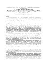
Effects of surface finish on high frequency signal - Taconic
Effects of surface finish on high frequency signal - Taconic
Effects of surface finish on high frequency signal - Taconic

Create successful ePaper yourself
Turn your PDF publications into a flip-book with our unique Google optimized e-Paper software.
EFFECTS OF SURFACE FINISH ON HIGH FREQUENCY SIGNAL LOSS<br />
USING VARIOUS SUBSTRATE MATERIALS<br />
D<strong>on</strong> Cullen Bruce Kline Gary Moderhock Larry Gatewood<br />
MacDermid, Inc.<br />
Tac<strong>on</strong>ic Omni-Circuits, Inc. Rockwell Collins, Inc.<br />
Waterbury, CT Petersburgh, NY Glenview, IL Cedar Rapids, IA<br />
ABSTRACT<br />
The amount <str<strong>on</strong>g>of</str<strong>on</strong>g> informati<strong>on</strong> transferred <strong>on</strong> wireless networks has increased dramatically with the tremendous growth <str<strong>on</strong>g>of</str<strong>on</strong>g><br />
mobile ph<strong>on</strong>es, Internet access, and hand held devices. In order to build the infrastructure needed to handle everincreasing<br />
data transfer, manufacturers <str<strong>on</strong>g>of</str<strong>on</strong>g> electr<strong>on</strong>ic devices turn to <strong>high</strong> speed, <strong>high</strong> <strong>frequency</strong> electr<strong>on</strong>ic <strong>signal</strong>s. The<br />
need to render these electr<strong>on</strong>ic devices portable is another technology driver. The merge <str<strong>on</strong>g>of</str<strong>on</strong>g> <strong>high</strong>-<strong>frequency</strong> <strong>signal</strong>s with<br />
small geometry c<strong>on</strong>ductive traces means that the topic <str<strong>on</strong>g>of</str<strong>on</strong>g> <strong>signal</strong> loss has reached a critical point in existing device<br />
producti<strong>on</strong>.<br />
The integrity <str<strong>on</strong>g>of</str<strong>on</strong>g> a <strong>high</strong>-<strong>frequency</strong> <strong>signal</strong> can be affected by several factors during Printed Circuit Board (PCB)<br />
c<strong>on</strong>structi<strong>on</strong>. The geometry <str<strong>on</strong>g>of</str<strong>on</strong>g> the c<strong>on</strong>ductor, the type <str<strong>on</strong>g>of</str<strong>on</strong>g> metallizati<strong>on</strong> used in/<strong>on</strong> the c<strong>on</strong>ductor, the <strong>signal</strong> <strong>frequency</strong>,<br />
the temperature <str<strong>on</strong>g>of</str<strong>on</strong>g> the substrate, and the type <str<strong>on</strong>g>of</str<strong>on</strong>g> dielectric material insulating the c<strong>on</strong>ductor all play an important role.<br />
Representatives <str<strong>on</strong>g>of</str<strong>on</strong>g> material supply, board fabricati<strong>on</strong>, and chemical process supply commenced a project to study some<br />
<str<strong>on</strong>g>of</str<strong>on</strong>g> the influential factors in more detail. A primary variable was the type <str<strong>on</strong>g>of</str<strong>on</strong>g> metallizati<strong>on</strong> used <strong>on</strong> the circuit board<br />
<str<strong>on</strong>g>surface</str<strong>on</strong>g>. Organic solderability preservative (OSP), hot air solder leveling (HASL), electroless nickel immersi<strong>on</strong> gold<br />
(ENIG), and immersi<strong>on</strong> silver were studied as PCB <str<strong>on</strong>g>surface</str<strong>on</strong>g> <str<strong>on</strong>g>finish</str<strong>on</strong>g> alternatives. Substrates under investigati<strong>on</strong> included<br />
woven glass PTFE, ceramic-filled woven glass PTFE, and FR4 epoxy as a c<strong>on</strong>trol. Specifically designed microstrip<br />
circuits were tested within a <strong>frequency</strong> range <str<strong>on</strong>g>of</str<strong>on</strong>g> 60 MHz to 26.0 GHz for <strong>signal</strong> loss across a range <str<strong>on</strong>g>of</str<strong>on</strong>g> PCB operating<br />
temperatures. At this stage, data was used to 10.0 GHz. C<strong>on</strong>tinuing studies will inspect data to 40 GHz.<br />
The results from the investigati<strong>on</strong> allow predicti<strong>on</strong> <str<strong>on</strong>g>of</str<strong>on</strong>g> <strong>signal</strong> loss characteristics across a broad <strong>frequency</strong> range when<br />
parts are re-designed to use alternative Pb-free <str<strong>on</strong>g>surface</str<strong>on</strong>g> <str<strong>on</strong>g>finish</str<strong>on</strong>g>es <strong>on</strong> PTFE substrates. The experimenters’ intent was to<br />
allow for a simple test usable by PCB fabricators to qualify their internal processes.<br />
INTRODUCTION<br />
Materials and Signal Loss<br />
The type <str<strong>on</strong>g>of</str<strong>on</strong>g> materials used in c<strong>on</strong>structing electr<strong>on</strong>ic<br />
circuits becomes more critical with the use <str<strong>on</strong>g>of</str<strong>on</strong>g> <strong>high</strong><br />
<strong>frequency</strong> <strong>signal</strong>s. The properties that most influence<br />
the <strong>signal</strong>s are related to the c<strong>on</strong>ductivity,<br />
permittivity (ε r ) and dissipati<strong>on</strong> factor (tan δ) <str<strong>on</strong>g>of</str<strong>on</strong>g> the<br />
materials. Ideally, the c<strong>on</strong>ductors should have low<br />
resistivity. In additi<strong>on</strong>, the shape, width, and<br />
thickness <str<strong>on</strong>g>of</str<strong>on</strong>g> the c<strong>on</strong>ductor trace should be c<strong>on</strong>sistent<br />
throughout the circuit path. C<strong>on</strong>versely, the substrate<br />
materials should be well insulating. The dielectric<br />
c<strong>on</strong>stant <str<strong>on</strong>g>of</str<strong>on</strong>g> the material should remain stable with<br />
increasing <strong>signal</strong> <strong>frequency</strong>. Through the selecti<strong>on</strong> <str<strong>on</strong>g>of</str<strong>on</strong>g><br />
proper materials, the dissipati<strong>on</strong> factor may be<br />
minimized. For productivity c<strong>on</strong>siderati<strong>on</strong>s,<br />
however, these material properties should be<br />
c<strong>on</strong>sidered al<strong>on</strong>g with other characteristics such as<br />
material availability, processability, and cost.<br />
In the current state <str<strong>on</strong>g>of</str<strong>on</strong>g> circuit board fabricati<strong>on</strong>, FR-4<br />
substrates are most comm<strong>on</strong>. Copper c<strong>on</strong>ductors <str<strong>on</strong>g>of</str<strong>on</strong>g><br />
communicati<strong>on</strong>s PCB’s are most comm<strong>on</strong>ly <str<strong>on</strong>g>finish</str<strong>on</strong>g>ed<br />
with ENIG. In this case, a <strong>high</strong> <strong>frequency</strong> <strong>signal</strong> may<br />
have significant loss due to 1) the dissipati<strong>on</strong> factor<br />
<str<strong>on</strong>g>of</str<strong>on</strong>g> FR-4 material, and 2) the resistivity <str<strong>on</strong>g>of</str<strong>on</strong>g> electroless<br />
nickel.<br />
Circuit Board Surface Finishes<br />
The selecti<strong>on</strong> <str<strong>on</strong>g>of</str<strong>on</strong>g> a board <str<strong>on</strong>g>finish</str<strong>on</strong>g> should be the result <str<strong>on</strong>g>of</str<strong>on</strong>g><br />
carefully balancing several demands 1 . It is important<br />
to c<strong>on</strong>sider the cost <str<strong>on</strong>g>of</str<strong>on</strong>g> the plating process. Thick<br />
electrolytic gold can have a large impact <strong>on</strong> the cost<br />
<str<strong>on</strong>g>of</str<strong>on</strong>g> the final electr<strong>on</strong>ic device. The chemical process<br />
needs to be widely available in order to satisfy the<br />
worldwide procurement demands <str<strong>on</strong>g>of</str<strong>on</strong>g> large OEM’s in<br />
the communicati<strong>on</strong> industry. Each shop must have<br />
competence in the chosen chemical plating process.<br />
Solderability, c<strong>on</strong>tact functi<strong>on</strong>ality and shelf-life <str<strong>on</strong>g>of</str<strong>on</strong>g><br />
the board are am<strong>on</strong>g other functi<strong>on</strong>al c<strong>on</strong>siderati<strong>on</strong>s<br />
<str<strong>on</strong>g>of</str<strong>on</strong>g> a <str<strong>on</strong>g>surface</str<strong>on</strong>g> <str<strong>on</strong>g>finish</str<strong>on</strong>g>. As the <strong>signal</strong> speed increases, the<br />
electrical properties <str<strong>on</strong>g>of</str<strong>on</strong>g> the coating may become the<br />
<strong>high</strong>est priority when selecting a board <str<strong>on</strong>g>finish</str<strong>on</strong>g>.<br />
Across the broad range <str<strong>on</strong>g>of</str<strong>on</strong>g> PCB manufacture, Hot Air<br />
Solder Level is the most comm<strong>on</strong>ly used board<br />
<str<strong>on</strong>g>finish</str<strong>on</strong>g>. In the HASL operati<strong>on</strong>, molten solder is<br />
applied to the circuitry by dip or c<strong>on</strong>veyorized<br />
applicati<strong>on</strong>. Excess solder is blown <str<strong>on</strong>g>of</str<strong>on</strong>g>f the circuitry<br />
with forced air. HASL use is limited by Lead (Pb)
estricti<strong>on</strong>s and by the <strong>high</strong>ly variable topography<br />
that results from HASL applicati<strong>on</strong>.<br />
Organic Solderability Preservatives (OSP’s) are thin<br />
organic coatings that are applied in vertical or<br />
c<strong>on</strong>veyorized chemical processes. The coating in not<br />
c<strong>on</strong>ductive, so OSP’s are not normally used for<br />
c<strong>on</strong>tact functi<strong>on</strong>al circuitry. The electrical <strong>signal</strong>s<br />
c<strong>on</strong>duct through the copper, so OSP’s are thought to<br />
have little effect <strong>on</strong> <strong>high</strong>-speed <strong>signal</strong>s.<br />
Electroless Nickel Immersi<strong>on</strong> Gold (ENIG) is a twolayer<br />
metallic coating over catalyzed copper. The top<br />
layer <str<strong>on</strong>g>of</str<strong>on</strong>g> gold provides low c<strong>on</strong>tact resistance,<br />
excellent shelf-life, and good wetting. The nickel<br />
provides a barrier layer to prevent copper and gold<br />
interdiffusi<strong>on</strong>. ENIG is deposited using a relatively<br />
complicated and costly vertical chemical process.<br />
Depending <strong>on</strong> electrical design <str<strong>on</strong>g>of</str<strong>on</strong>g> the PCB, <strong>signal</strong>s<br />
may need to travel through the nickel layer.<br />
Electroless nickel/phosphorous can have undesirable<br />
magnetic properties and is less c<strong>on</strong>ductive than<br />
copper, gold or silver. The integrity <str<strong>on</strong>g>of</str<strong>on</strong>g> a <strong>high</strong> speed<br />
<strong>signal</strong> may depend <strong>on</strong> the thickness <str<strong>on</strong>g>of</str<strong>on</strong>g> the nickel<br />
layer and the porti<strong>on</strong> <str<strong>on</strong>g>of</str<strong>on</strong>g> the c<strong>on</strong>ductor through which<br />
the <strong>signal</strong> travels.<br />
Table 1 - Resistivity <str<strong>on</strong>g>of</str<strong>on</strong>g> PCB Metals 2,3,4<br />
Copper<br />
1.7 µΩ.cm<br />
Gold<br />
2.4 µΩ.cm<br />
Nickel<br />
7.4 µΩ.cm<br />
Electroless Nickel Phos. 55-90 µΩ.cm<br />
Silver<br />
1.6 µΩ.cm<br />
Tin<br />
10.9 µΩ.cm<br />
Sn60Pb40 Solder<br />
17.0 µΩ.cm<br />
Immersi<strong>on</strong> Silver c<strong>on</strong>sists <str<strong>on</strong>g>of</str<strong>on</strong>g> a very thin (0.15-0.50<br />
micrometer) coating <str<strong>on</strong>g>of</str<strong>on</strong>g> nearly pure silver. Organic<br />
materials are typically codepoited within the silver<br />
for preventi<strong>on</strong> <str<strong>on</strong>g>of</str<strong>on</strong>g> tarnish and electromigrati<strong>on</strong>. The<br />
metal coating is deposited via a relatively simple and<br />
inexpensive c<strong>on</strong>veyorized or vertical chemical<br />
process. Silver is the most c<strong>on</strong>ductive element and<br />
c<strong>on</strong>sists <str<strong>on</strong>g>of</str<strong>on</strong>g> <strong>on</strong>ly the outermost coating <strong>on</strong> the<br />
c<strong>on</strong>ductor. The belief is that silver will not have a<br />
significant effect <strong>on</strong> <strong>high</strong>-speed <strong>signal</strong>s because <str<strong>on</strong>g>of</str<strong>on</strong>g> its<br />
negligible thickness relative to skin thickness. The<br />
benefit <str<strong>on</strong>g>of</str<strong>on</strong>g> silver relative to other PCB coatings lies in<br />
its flat topography for <strong>high</strong> density circuit designs<br />
and its functi<strong>on</strong>ality as a c<strong>on</strong>tact <str<strong>on</strong>g>surface</str<strong>on</strong>g>.<br />
The thickness <str<strong>on</strong>g>of</str<strong>on</strong>g> the board <str<strong>on</strong>g>finish</str<strong>on</strong>g> coatings is<br />
increasingly important with <strong>high</strong>er <strong>frequency</strong> <strong>signal</strong>s<br />
due to the “skin depth” <str<strong>on</strong>g>of</str<strong>on</strong>g> the current flowing through<br />
the PCB trace “transmissi<strong>on</strong> line.” The skin depth<br />
varies with the <strong>frequency</strong> <str<strong>on</strong>g>of</str<strong>on</strong>g> the <strong>signal</strong> and the<br />
material <str<strong>on</strong>g>of</str<strong>on</strong>g> the c<strong>on</strong>ductor, and is defined as the<br />
distance in the c<strong>on</strong>ductor at which the electric field<br />
has decreased to 30% <str<strong>on</strong>g>of</str<strong>on</strong>g> the value at the <str<strong>on</strong>g>surface</str<strong>on</strong>g>. 5<br />
10<br />
1<br />
0.1<br />
0.30 10.00 300.00<br />
Frequency (GHz)<br />
Figure 1: Skin Depth with Increasing GHz 5<br />
High Speed Laminate Materials<br />
The need for circuits capable <str<strong>on</strong>g>of</str<strong>on</strong>g> operating at<br />
frequencies over 2GHz has motivated designers to<br />
c<strong>on</strong>sider materials other then traditi<strong>on</strong>al FR-4.<br />
Alternative materials have been integrated into either<br />
pure or multi-layer mixed dielectric packages capable<br />
<str<strong>on</strong>g>of</str<strong>on</strong>g> providing <strong>high</strong>speed digital, RF/microwave, or<br />
combined circuit functi<strong>on</strong>ality.<br />
To characterize the <str<strong>on</strong>g>surface</str<strong>on</strong>g> <str<strong>on</strong>g>finish</str<strong>on</strong>g>’s loss performance<br />
with alternative dielectric materials, three substrate<br />
types were investigated, covering a range <str<strong>on</strong>g>of</str<strong>on</strong>g> dielectric<br />
and loss performance. Table 2 details the primary<br />
characteristics <str<strong>on</strong>g>of</str<strong>on</strong>g> the substrate materials. The<br />
materials chosen c<strong>on</strong>sist <str<strong>on</strong>g>of</str<strong>on</strong>g> an epoxy/ woven glass<br />
(FR-4), a ceramic filled PTFE/ woven glass (RF-35),<br />
and a PTFE/ woven glass (TLY-5). To insure<br />
c<strong>on</strong>sistent results, each material type investigated<br />
utilized a base thickness <str<strong>on</strong>g>of</str<strong>on</strong>g> 0.020”, clad both sides<br />
with <strong>on</strong>e-ounce ED copper foil.<br />
Table 2:Laminate Material Properties<br />
Property FR-4 RF-35 TLY-5<br />
Permittivity* 4.8+/-0.2 3.5+/-0.1 2.2+/- 0.02<br />
Dissipati<strong>on</strong> 0.02 0.0027 0.0009<br />
Factor *<br />
Moisture 0.20% 0.02% 0.02%<br />
Absorpti<strong>on</strong><br />
Peel Strength > 8.0 >10.0 >12.0<br />
lbs/inch<br />
Flammability 94V-0 94V-0 94V-0<br />
*Permittivity and Dissipati<strong>on</strong> at 1.5 - 2.0 GHz.<br />
EXPERIMENTAL<br />
To characterize losses due to <str<strong>on</strong>g>surface</str<strong>on</strong>g> <str<strong>on</strong>g>finish</str<strong>on</strong>g>, a 50-ohm<br />
copper microstrip was fabricated <strong>on</strong> the three types <str<strong>on</strong>g>of</str<strong>on</strong>g><br />
substrate materials and measured across a range <str<strong>on</strong>g>of</str<strong>on</strong>g><br />
frequencies for inserti<strong>on</strong> loss in decibels. The same<br />
50-ohm test circuit was used for all test coup<strong>on</strong>s <str<strong>on</strong>g>of</str<strong>on</strong>g><br />
the selected material. The c<strong>on</strong>ductor design was
altered for each substrate material according to each<br />
material’s dielectric properties. Loss characteristics<br />
from the five <str<strong>on</strong>g>surface</str<strong>on</strong>g> <str<strong>on</strong>g>finish</str<strong>on</strong>g>es (OSP, HASL, low<br />
ENIG, <strong>high</strong> ENIG, and immersi<strong>on</strong> silver) were<br />
compared.<br />
Test Vehicle Fabricati<strong>on</strong><br />
Process panels were grouped by material type and<br />
were drilled and plated in the same set up. Omni<br />
Circuits Inc. manufactured the test vehicle. Omni<br />
panel plates using an automated Uniplate horiz<strong>on</strong>tal<br />
line and Atotech electrolytic copper chemistry.<br />
Material was 0.020 1/1 oz. copper clad laminate.<br />
Another 1.2 mils (approximately 1.0 mils inside the<br />
via holes) was plated <strong>on</strong> to the <str<strong>on</strong>g>surface</str<strong>on</strong>g>. Reference<br />
cross-secti<strong>on</strong>al photos Figures Appendix A1a-A5c.<br />
Panel preparati<strong>on</strong> c<strong>on</strong>sisted <str<strong>on</strong>g>of</str<strong>on</strong>g> a micro-etch pre-clean<br />
followed by pumice scrub and dry-film applicati<strong>on</strong>.<br />
Panels were exposed using the same top film for all<br />
panels <str<strong>on</strong>g>of</str<strong>on</strong>g> the same material. A coup<strong>on</strong> identificati<strong>on</strong><br />
legend was added in the copper <str<strong>on</strong>g>of</str<strong>on</strong>g> the ground plane.<br />
Panels were then developed and etched with cupric<br />
chloride. A horiz<strong>on</strong>tal Schmidd etcher was used for<br />
its capability to maintain line width integrity <str<strong>on</strong>g>of</str<strong>on</strong>g> the<br />
50-ohm microstrip. The <str<strong>on</strong>g>surface</str<strong>on</strong>g> <str<strong>on</strong>g>finish</str<strong>on</strong>g>es were<br />
applied as follows:<br />
Panels were CNC routed to depanelize test coup<strong>on</strong>s.<br />
No solder mask or other types <str<strong>on</strong>g>of</str<strong>on</strong>g> <str<strong>on</strong>g>surface</str<strong>on</strong>g> protecti<strong>on</strong><br />
were added.<br />
Electrical Measurement<br />
Electrical measurements were c<strong>on</strong>ducted at Rockwell<br />
Collins, Inc. For this set <str<strong>on</strong>g>of</str<strong>on</strong>g> experiments, the test<br />
specimen was a 50-ohm microstrip transmissi<strong>on</strong> line.<br />
Each coup<strong>on</strong> was mounted in a test apparatus that<br />
c<strong>on</strong>sisted <str<strong>on</strong>g>of</str<strong>on</strong>g> an aluminum carrier plate and stainlesssteel<br />
SMA c<strong>on</strong>nectors. The c<strong>on</strong>nectors (rated to 18<br />
GHz with 20-mil flat tabs) were soldered to the test<br />
specimen. An HP8510 vector network analyzer with<br />
TDR (time-domain reflectometry) was used to collect<br />
full, two-port S-parameters and account for the<br />
c<strong>on</strong>tributi<strong>on</strong> <str<strong>on</strong>g>of</str<strong>on</strong>g> the test apparatus. HP test apparatus<br />
is shown in Figure 2.<br />
OSP: Two panels <str<strong>on</strong>g>of</str<strong>on</strong>g> each material were processed<br />
through a horiz<strong>on</strong>tal line using Shipley R<strong>on</strong>al’s<br />
R<strong>on</strong>acoat chemistry. Preparati<strong>on</strong> c<strong>on</strong>sisted <str<strong>on</strong>g>of</str<strong>on</strong>g> preclean<br />
and microetch.<br />
HASL: Two panels <str<strong>on</strong>g>of</str<strong>on</strong>g> each were processed in a<br />
Gyrex vertical Hot Air Solder Leveling machine.<br />
Preparati<strong>on</strong> c<strong>on</strong>sisted <str<strong>on</strong>g>of</str<strong>on</strong>g> micro-etch/ pre-clean<br />
followed by a <str<strong>on</strong>g>surface</str<strong>on</strong>g> activator. Panels were postbaked<br />
after solder coat.<br />
Low ENIG: Two panels each were process<br />
through a vertical dip immersi<strong>on</strong> Shipley R<strong>on</strong>al<br />
nickel/gold line with agitati<strong>on</strong>. Nickel thickness was<br />
targeted at 50 µinches. XRF equipment was used to<br />
verify the mean nickel thickness <str<strong>on</strong>g>of</str<strong>on</strong>g> 57.7 µinches.<br />
The mean gold was measured at 6.2 µinches.<br />
High ENIG: Same as above except nickel<br />
thickness was targeted at 200 microinches. XRF<br />
equipment was used to verify the mean nickel<br />
thickness 197.5 µinches. On this sample set, mean<br />
gold thickness was determined to be 4.9 µinches.<br />
Immersi<strong>on</strong> Silver: Two panels were processed<br />
through a vertical dip MacDermid Sterling<br />
immersi<strong>on</strong> silver process with agitati<strong>on</strong>. Immersi<strong>on</strong><br />
silver thickness was determined by XRF to be 8 –12<br />
µinches.<br />
Figure 2: Measurement Apparatus<br />
The test method c<strong>on</strong>sisted <str<strong>on</strong>g>of</str<strong>on</strong>g> visual inspecti<strong>on</strong>,<br />
physical measurements, system calibrati<strong>on</strong>, test<br />
apparatus/ circuit validati<strong>on</strong>, and electrical data<br />
collecti<strong>on</strong>. Each specimen was visually inspected<br />
with the naked eye as well as under a microscope to<br />
ensure there was no damage. In additi<strong>on</strong>, physical<br />
measurements (line widths) were taken to ensure the<br />
microstrip lines were etched to within an acceptable<br />
tolerance to yield a good 50-ohm line. Some<br />
anomalies found at this stage appeared to be<br />
dependent <strong>on</strong> imaging and plating quality.<br />
The measurement system was calibrated using a<br />
3.5mm calibrati<strong>on</strong> kit. Each test specimen was<br />
mounted in a test apparatus and c<strong>on</strong>nected to the<br />
measurement system. TDR measurements were used<br />
to validate the performance <str<strong>on</strong>g>of</str<strong>on</strong>g> the coax-to-microstrip<br />
transiti<strong>on</strong>s. The loss c<strong>on</strong>tributi<strong>on</strong> due to the<br />
c<strong>on</strong>nectors was verified to be so small enough that it<br />
wasn’t necessary to gate its resp<strong>on</strong>se out <str<strong>on</strong>g>of</str<strong>on</strong>g> the
measurement. Likewise, the return loss (S11 and<br />
S22) <str<strong>on</strong>g>of</str<strong>on</strong>g> each specimen revealed that the mismatch<br />
losses were negligible. The final step was to collect<br />
the total inserti<strong>on</strong> loss data (S21) and mathematically<br />
manipulate it by the length <str<strong>on</strong>g>of</str<strong>on</strong>g> the line to yield loss<br />
per unit length data as a functi<strong>on</strong> <str<strong>on</strong>g>of</str<strong>on</strong>g> <strong>frequency</strong>.<br />
Inserti<strong>on</strong> Loss (dB/inch) =<br />
20 x LOG ([SQRT (S21 2 real +S21 2 imag)] / 5.02<br />
The figure-<str<strong>on</strong>g>of</str<strong>on</strong>g>-merit collected was the total inserti<strong>on</strong><br />
loss <str<strong>on</strong>g>of</str<strong>on</strong>g> a 5-inch line, with final data presented as<br />
dB/inch vs. GHz. Figure 3 dem<strong>on</strong>strates the test<br />
specimen c<strong>on</strong>necti<strong>on</strong>.<br />
The averages for each variable set were collected into<br />
the summary chart Figures 4-6.<br />
dB/Inch<br />
1.00<br />
0.80<br />
0.60<br />
0.40<br />
0.20<br />
0.00<br />
Inserti<strong>on</strong> Loss vs. Frequency<br />
FR-4<br />
0.0 2.0 4.0 6.0 8.0 10.0<br />
GHz<br />
Chart Order:<br />
High ENIG<br />
Silver<br />
Low ENIG<br />
HASL<br />
OSP<br />
Figure 4: Loss vs. Frequency <strong>on</strong> FR-4 material<br />
dB/Inch<br />
0.40<br />
0.30<br />
0.20<br />
0.10<br />
Inserti<strong>on</strong> Loss vs. Frequency<br />
RF-35<br />
Chart Order:<br />
High ENIG<br />
Silver<br />
HASL<br />
Low ENIG<br />
OSP<br />
Figure 3: Test Board Measurement<br />
In future experiments, the test specimen, apparatus,<br />
and methodology will be refined to collect more<br />
comprehensive data. The test specimen will include<br />
res<strong>on</strong>ator structures that will allow differentiati<strong>on</strong><br />
am<strong>on</strong>g c<strong>on</strong>ductor and dielectric losses. Also, a more<br />
sophisticated test apparatus with custom calibrati<strong>on</strong><br />
standards will yield greater accuracy, repeatability,<br />
and efficiency. Additi<strong>on</strong>al refinements to the test<br />
methodology/ procedure will enable the efficient<br />
collecti<strong>on</strong> <str<strong>on</strong>g>of</str<strong>on</strong>g> electrical performance parameters in to<br />
the millimeter wave <strong>frequency</strong> range.<br />
RESULTS AND DISCUSSION<br />
Data were gathered and evaluated to ensure statistical<br />
significance. For each test board, 400 datapoints<br />
were collected. Further, 3 boards were measured <str<strong>on</strong>g>of</str<strong>on</strong>g><br />
each <str<strong>on</strong>g>finish</str<strong>on</strong>g> to form an average. Overall, 36,000<br />
datapoints were recorded and analyzed. The series <str<strong>on</strong>g>of</str<strong>on</strong>g><br />
data from TLY-5 material plated with High ENIG<br />
had to be discarded due to improper sample handling.<br />
The summary data set is presented as Table 3.<br />
Table 3: Substrate and Finish Loss (dB/inch)<br />
loss at 10GHz ∆ due to PCB <str<strong>on</strong>g>finish</str<strong>on</strong>g><br />
FR-4 0.80 – 0.89 0.086 (10.2 %)<br />
RF-35 0.31 – 0.33 0.020 (6.2 %)<br />
TLY-5 0.20 – 0.24 0.037 (16.7 %)<br />
0.00<br />
0.0 2.0 4.0 6.0 8.0 10.0<br />
GHz<br />
Figure 5: Loss vs. Frequency <strong>on</strong> RF-35 material<br />
dB/Inch<br />
0.30<br />
0.20<br />
0.10<br />
0.00<br />
Inserti<strong>on</strong> Loss vs. Frequency<br />
TLY-5<br />
0.0 2.0 4.0 6.0 8.0 10.0<br />
GHz<br />
Chart Order:<br />
Silver<br />
HASL<br />
Low ENIG<br />
OSP<br />
Figure 6: Loss vs. Frequency <strong>on</strong> TLY-5 material<br />
The inserti<strong>on</strong> loss from samples manufactured with<br />
FR-4 material was calculated to be about 0.84<br />
dB/inch at 10GHz. The variati<strong>on</strong> due to <str<strong>on</strong>g>surface</str<strong>on</strong>g><br />
<str<strong>on</strong>g>finish</str<strong>on</strong>g> at <strong>high</strong> <strong>frequency</strong> was 0.0860 db/inch (10.2%).<br />
The inserti<strong>on</strong> loss from samples manufactured with<br />
RF-35 material was calculated to be about 0.32<br />
dB/inch at 10GHz. The variati<strong>on</strong> due to <str<strong>on</strong>g>surface</str<strong>on</strong>g><br />
<str<strong>on</strong>g>finish</str<strong>on</strong>g> at <strong>high</strong> <strong>frequency</strong> was 0.0198 db/inch (6.2%).
The inserti<strong>on</strong> loss from samples manufactured with<br />
TLY-5 material was calculated to be about 0.22<br />
dB/inch at 10GHz. The variati<strong>on</strong> due to <str<strong>on</strong>g>surface</str<strong>on</strong>g><br />
<str<strong>on</strong>g>finish</str<strong>on</strong>g> at <strong>high</strong> <strong>frequency</strong> was 0.0372 db/inch (16.7%).<br />
An increasing amount <str<strong>on</strong>g>of</str<strong>on</strong>g> ripple in the <strong>signal</strong> was<br />
found above 6 GHz. TDR analysis yielded insight<br />
into the locati<strong>on</strong> <str<strong>on</strong>g>of</str<strong>on</strong>g> the ripple’s cause within the<br />
microstrip coup<strong>on</strong>s. Surface irregularities such as the<br />
plating defect in Figure 7 were determined to affect<br />
the <strong>signal</strong>. This defect was assigned to an imaging<br />
problem and is representative <str<strong>on</strong>g>of</str<strong>on</strong>g> the type <str<strong>on</strong>g>of</str<strong>on</strong>g> defect<br />
that becomes troublesome as <strong>high</strong> <strong>frequency</strong> <strong>signal</strong>s<br />
are applied.<br />
CONCLUSIONS<br />
The following observati<strong>on</strong>s were made as<br />
c<strong>on</strong>clusi<strong>on</strong>s to this experiment:<br />
• Signal <strong>frequency</strong> variati<strong>on</strong>, as expected, had the<br />
primary influence <strong>on</strong> loss measurements. All<br />
substrate materials and microstrip plating<br />
<str<strong>on</strong>g>finish</str<strong>on</strong>g>es suffered from loss in <strong>signal</strong> integrity as<br />
<strong>signal</strong> <strong>frequency</strong> increased. The maximum loss<br />
due to <strong>signal</strong> increase was <strong>on</strong> FR-4 plated with<br />
High ENIG. Nearly 0.9 db/inch was observed at<br />
10 GHz. More than 1.6 db/inch was measured at<br />
18 GHz (the rated limit <str<strong>on</strong>g>of</str<strong>on</strong>g> the c<strong>on</strong>nector used)<br />
but this data was discarded until improved<br />
apparatus is installed.<br />
• The substrate material had a pr<str<strong>on</strong>g>of</str<strong>on</strong>g>ound effect <strong>on</strong><br />
inserti<strong>on</strong> loss measurements. The variati<strong>on</strong> in<br />
inserti<strong>on</strong> loss due to the selecti<strong>on</strong> <str<strong>on</strong>g>of</str<strong>on</strong>g> board<br />
substrate was <strong>on</strong> the order <str<strong>on</strong>g>of</str<strong>on</strong>g> 0.6 dB/inch. The<br />
substrate material and its loss tangent should be<br />
the basis for establishing the loss range within<br />
which the circuit is capable <str<strong>on</strong>g>of</str<strong>on</strong>g> functi<strong>on</strong>ing.<br />
Figure 7: Line Width Irregularity affecting Signal<br />
Statistical Analysis<br />
Data points were extracted from the loss analysis <str<strong>on</strong>g>of</str<strong>on</strong>g><br />
each material ranging from 1-10 GHz and placed in a<br />
block format. The data for each material type was<br />
analyzed using Anova to validate if <strong>frequency</strong> and<br />
<str<strong>on</strong>g>surface</str<strong>on</strong>g> <str<strong>on</strong>g>finish</str<strong>on</strong>g> supported the hypotheses. The<br />
measurements for all three material types c<strong>on</strong>cluded<br />
that <strong>frequency</strong> and <str<strong>on</strong>g>surface</str<strong>on</strong>g> <str<strong>on</strong>g>finish</str<strong>on</strong>g> were significant<br />
variables, producing F statistics well above the F-<br />
critical values.<br />
FR-4 F-value F-critical<br />
Surface Finish 18.74 2.86<br />
Frequency 3272.55 2.71<br />
RF-35 F-value F-critical<br />
Surface Finish 21.05 2.86<br />
Frequency 2898.12 2.71<br />
TLY-5 F-value F-Critical<br />
Surface Finish 9.90 3.29<br />
Frequency 587.04 2.90<br />
Figure 8: ANOVA Significance <str<strong>on</strong>g>of</str<strong>on</strong>g> Variables<br />
• The <str<strong>on</strong>g>surface</str<strong>on</strong>g> <str<strong>on</strong>g>finish</str<strong>on</strong>g>es had less influence <strong>on</strong> loss<br />
characteristics than expected. Anecdotally, our<br />
team expected the High ENIG <str<strong>on</strong>g>surface</str<strong>on</strong>g> to be<br />
substantially more lossy than all other <str<strong>on</strong>g>finish</str<strong>on</strong>g>es.<br />
In fact, all <str<strong>on</strong>g>surface</str<strong>on</strong>g> <str<strong>on</strong>g>finish</str<strong>on</strong>g>es were measured to<br />
within 0.1 dB/inch even at 10GHz. The<br />
expectati<strong>on</strong> at <strong>high</strong>er frequencies is that the EN<br />
barrier will begin to show more pr<str<strong>on</strong>g>of</str<strong>on</strong>g>ound losses<br />
compared to other <str<strong>on</strong>g>finish</str<strong>on</strong>g>es. Updated informati<strong>on</strong><br />
will be presented for <strong>high</strong>er frequencies at the<br />
time <str<strong>on</strong>g>of</str<strong>on</strong>g> presentati<strong>on</strong>.<br />
• Surface <str<strong>on</strong>g>finish</str<strong>on</strong>g> selecti<strong>on</strong> became more important<br />
with <strong>high</strong>er <strong>frequency</strong>. The difference in<br />
inserti<strong>on</strong> loss am<strong>on</strong>g board <str<strong>on</strong>g>finish</str<strong>on</strong>g>es was within<br />
0.0072 db/inch at 0.06 GHz, while the delta was<br />
more than 10 times as large, 0.0860 dB/inch at<br />
10GHz. On a 5 inch PCB trace, the loss<br />
accumulates to a total <str<strong>on</strong>g>of</str<strong>on</strong>g> 0.43 dB, a value as<br />
important as loss due to substrate material.<br />
• The use <str<strong>on</strong>g>of</str<strong>on</strong>g> OSP and HASL is widespread in the<br />
electr<strong>on</strong>ics industry. There has been some<br />
questi<strong>on</strong> as to the effect <str<strong>on</strong>g>of</str<strong>on</strong>g> new <str<strong>on</strong>g>finish</str<strong>on</strong>g>es such as<br />
Immersi<strong>on</strong> Silver with <strong>high</strong> <strong>frequency</strong> <strong>signal</strong>s.<br />
The data supports the hypothesis that the Silver<br />
has little effect <strong>on</strong> <strong>signal</strong> loss due to the<br />
c<strong>on</strong>ductivity and thinness <str<strong>on</strong>g>of</str<strong>on</strong>g> the Silver coating.<br />
• Electroless nickel has a detrimental influence <strong>on</strong><br />
<strong>signal</strong> c<strong>on</strong>servati<strong>on</strong>. The effect <str<strong>on</strong>g>of</str<strong>on</strong>g> EN appears to<br />
increase at <strong>high</strong>er frequencies. ENIG coatings as<br />
deposited in standard practice (High ENIG in<br />
this experiment) dem<strong>on</strong>strate substantial <strong>signal</strong><br />
loss above 5 GHz. Lower thickness EN coatings
effectively extended the <strong>frequency</strong> range at<br />
which the microstrips were functi<strong>on</strong>al. Lower<br />
thickness EN may be appropriate for some<br />
electr<strong>on</strong>ic devices, but may be inadequate for<br />
other applicati<strong>on</strong>s. At the time <str<strong>on</strong>g>of</str<strong>on</strong>g> this article’s<br />
publicati<strong>on</strong>, the comm<strong>on</strong> EN minimum thickness<br />
specificati<strong>on</strong> was 120 microinch (3 micrometer).<br />
6. B.Hought<strong>on</strong>; “Alternative Metallic PWB<br />
Finishes: an Update <strong>on</strong> the ITRI/ October<br />
Project.” IPC Expo, (March 1998)<br />
• Selecti<strong>on</strong> <str<strong>on</strong>g>of</str<strong>on</strong>g> a PCB <str<strong>on</strong>g>surface</str<strong>on</strong>g> <str<strong>on</strong>g>finish</str<strong>on</strong>g> will depend <strong>on</strong><br />
several factors. HASL may not meet comp<strong>on</strong>ent<br />
density limits. OSP’s insulating characteristics<br />
may restrict its use in some communicati<strong>on</strong>s<br />
devices relying <strong>on</strong> <str<strong>on</strong>g>surface</str<strong>on</strong>g> c<strong>on</strong>tact c<strong>on</strong>ductivity.<br />
ENIG, a clear choice for many handheld<br />
communicati<strong>on</strong>s devices, may become restricted<br />
due to its variability in loss performance and<br />
impact <strong>on</strong> <strong>high</strong> <strong>frequency</strong> <strong>signal</strong>s. Immersi<strong>on</strong><br />
silver appears to meet many <str<strong>on</strong>g>of</str<strong>on</strong>g> the functi<strong>on</strong>s<br />
required <str<strong>on</strong>g>of</str<strong>on</strong>g> future PCB designs.<br />
• The c<strong>on</strong>ductor shape, line width c<strong>on</strong>sistency, and<br />
etching quality <str<strong>on</strong>g>of</str<strong>on</strong>g> PCB fabricati<strong>on</strong> steps becomes<br />
increasingly important when studying <strong>high</strong><strong>frequency</strong><br />
<strong>signal</strong>s. In additi<strong>on</strong>, the pr<str<strong>on</strong>g>of</str<strong>on</strong>g>ile <str<strong>on</strong>g>of</str<strong>on</strong>g> the<br />
copper foil cladding the dielectric material (as<br />
documented in Appendix Figures A6 a-c) will<br />
affect performance. The electrical testing<br />
method described in this experiment is relatively<br />
simple and may be applied at PCB fabricati<strong>on</strong><br />
shops as a support for their OEM customers’<br />
design departments.<br />
ACKNOWLEDGEMENTS<br />
The authors wish to express their appreciati<strong>on</strong> and<br />
admirati<strong>on</strong> <str<strong>on</strong>g>of</str<strong>on</strong>g> the expert engineers participating in<br />
this study. Dan Ash and L<strong>on</strong>nie Cott<strong>on</strong> <str<strong>on</strong>g>of</str<strong>on</strong>g><br />
Powerwave Technologies advised us <strong>on</strong> critical<br />
measurements and sample c<strong>on</strong>structi<strong>on</strong>. Christina<br />
C<strong>on</strong>way and Mike Davids<strong>on</strong> <str<strong>on</strong>g>of</str<strong>on</strong>g> Rockwell Collins<br />
were instrumental in providing mechanical and<br />
electrical measurements. Mary King and Ed<br />
Komarnicki <str<strong>on</strong>g>of</str<strong>on</strong>g> MacDermid provided <str<strong>on</strong>g>surface</str<strong>on</strong>g> analysis<br />
and cross-secti<strong>on</strong> photography.<br />
REFERENCES<br />
1. D.Cullen; “HASL Alternatives.” PC<br />
Fabricati<strong>on</strong>, (July 1999)<br />
2. C.Harper, R.Samps<strong>on</strong>. Electr<strong>on</strong>ic Materials &<br />
Processes Handbook; McGraw-Hill, 1994.<br />
3. G.Mallory. Electroless Plating; 1990 AESF<br />
Publicati<strong>on</strong>s.<br />
4. W.Safranek, Properties <str<strong>on</strong>g>of</str<strong>on</strong>g> Electrodeposited<br />
Metals and Alloys. 1986 AESF Publicati<strong>on</strong>s.<br />
5. A.Scott. Understanding Microwaves; Wiley,<br />
1993.
APPENDIX A: Microstrip Cross-Secti<strong>on</strong>s<br />
..<br />
Figure A1 a-c: HASL <strong>on</strong> FR-4, RF-35, and TLY-5 (500X)<br />
.. ..<br />
Figure A2 a-c: OSP <strong>on</strong> FR-4, RF-35, and TLY-5 (500X)<br />
..<br />
Figure A3 a-c: “Low” Nickel Gold <strong>on</strong> FR-4, RF-35, and TLY-5 (500X)<br />
Figure A4 a-c: “High” Nickel Gold <strong>on</strong> FR-4, RF-35, and TLY-5 (500X)<br />
Figure A5 a-c: Immersi<strong>on</strong> Silver <strong>on</strong> FR-4, RF-35, and TLY-5 (500X)
.<br />
Figure A6 a-c: Copper Foil Pr<str<strong>on</strong>g>of</str<strong>on</strong>g>ile <str<strong>on</strong>g>of</str<strong>on</strong>g> the Substrates: FR-4, RF-35, and TLY-5 (2000X)