A Comprehensive Study of Dilute Magnetic ... - OPUS Würzburg
A Comprehensive Study of Dilute Magnetic ... - OPUS Würzburg
A Comprehensive Study of Dilute Magnetic ... - OPUS Würzburg

You also want an ePaper? Increase the reach of your titles
YUMPU automatically turns print PDFs into web optimized ePapers that Google loves.
28 2. Resonant tunneling in all II-VI semiconductor devices<br />
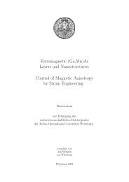
a)<br />
0.20<br />
b)<br />
E res eV<br />
0.15<br />
0.10<br />
0.05<br />
0.00<br />
6 8 10 12<br />
d qw nm<br />
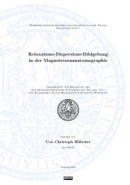
d/nm material doping/cm -3<br />
10+10+30 Al+Ti+Au<br />
30 ZnSe 2·10^19<br />
15 Zn(0.97)Be(0.03)Se 1·10^18<br />
10 ZnSe i<br />
6 Zn(0.8)Be(0.2)Se i<br />
d qw Zn(0.92)Mn(0.08)Se i<br />
6 Zn(0.8)Be(0.2)Se i<br />
10 ZnSe i<br />
10 Zn(0.97)Be(0.03)Se 1·10^18<br />
100 ZnSe 2·10^19<br />
300 Zn(0.97)Be(0.03)Se 2·10^19<br />
20 Zn(0.9)Be(0.1)Se i<br />
50 ZnSe i<br />
200 Zn(0.97)Be(0.03)Se 2·10^19<br />
buffer GaAs i<br />
substrate GaAs:Si 1.5·10 18<br />
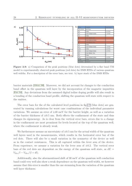
Figure 2.9: a) Comparison <strong>of</strong> the peak positions (blue dots) determined by a flat band TM<br />
model to experimentally observed peak positions (red dots) for DMS RTDs <strong>of</strong> various quantum<br />
well widths. For a description <strong>of</strong> the error bars, see text. b) layer stack <strong>of</strong> the DMS RTDs<br />
barrier materials [Ohno 90]. Moreover, we did not account for changes to the conduction<br />
band <strong>of</strong>fset in the quantum well layer by the incorporation <strong>of</strong> the magnetic impurities<br />
[Dai 94]. Any deviations from the assumed digital iodine doping pr<strong>of</strong>ile will also result in<br />
a bending <strong>of</strong> the conduction band pr<strong>of</strong>ile, shifting the quantum well state with respect to<br />
the emitter.<br />
The error bars for the <strong>of</strong> the calculated level positions in fig.2.9 (blue dots) are generated<br />
by running calculations for worst case combinations <strong>of</strong> the individual parameter<br />
variations. We assume an error <strong>of</strong> ±40 meV for the barrier height, as well as a variation<br />
<strong>of</strong> the barrier thickness <strong>of</strong> ±0.5 nm. Both effects the confinement <strong>of</strong> the state and thus<br />
changes its eigenenergy. As is clear from the vertical error bars, errors due to a change<br />
in the confinement are most prominent for levels located at the top <strong>of</strong> the quantum well,<br />
where the confinement is already weak.<br />
We furthermore assume an uncertainty <strong>of</strong> ±0.5 nm for the actual width <strong>of</strong> the quantum<br />
well layers used in the measurements, which results in the horizontal error bar <strong>of</strong> the<br />
red dots. There will also be a small variation in the symmetry <strong>of</strong> the device as well<br />
as in the contact resistances. This is all captured within the lever arm <strong>of</strong> the device.<br />
From experience, we assume a variation for the lever arm <strong>of</strong> ±0.2. The vertical error<br />
bars <strong>of</strong> the red dots are dependent on the energy <strong>of</strong> the quantum well state, as dE =<br />
V Res /l − V Res /(l + dl).<br />
Additionally, also the aforementioned shift <strong>of</strong> 30 meV <strong>of</strong> the quantum well conduction<br />
band could very well also show a weak dependence on the quantum well width, we however<br />
assume that this error is smaller than the one stemming from the variation <strong>of</strong> the quantum<br />
well layer thickness.