A Comprehensive Study of Dilute Magnetic ... - OPUS Würzburg
A Comprehensive Study of Dilute Magnetic ... - OPUS Würzburg
A Comprehensive Study of Dilute Magnetic ... - OPUS Würzburg

Create successful ePaper yourself
Turn your PDF publications into a flip-book with our unique Google optimized e-Paper software.
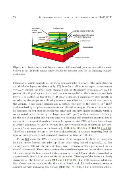
78 6. Fermi-edge singularity in a non-magnetic SAD RTD<br />
high doped<br />
n-ZnSe<br />
contact layers<br />
resonant<br />
tunneling<br />
in-situ contact<br />
i-ZnSe collector and emitter<br />
self assembled CdSe qdots<br />
with (Zn,Be)Se barriers<br />
ex-situ contact<br />
ZnBeSe Buffer<br />
GaAs substrate<br />
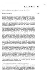
Figure 6.2: Device layout and layer structure. Self assembled quantum dots which are embedded<br />
in the (Zn,Be)Se tunnel barrier provide the resonant state for the tunneling transport<br />
mechanism.<br />
formation <strong>of</strong> ohmic contacts at the metal-semiconductor interface. The layer structure<br />
and the device layout are shown in fig. 6.2. In order to allow for transport measurements<br />
vertically through the layer stack, standard optical lithography techniques are used to<br />
pattern 10 x 10 µm 2 square pillars, and contacts are applied to the bottom and top ZnSe<br />
layers. The contact on top <strong>of</strong> the RTD pillar is deposited immediately after growth by<br />
transferring the sample to a ultra-high-vacuum metallization chamber without breaking<br />
the vacuum. It has ohmic behavior and a contact resistance on the order <strong>of</strong> 10 −3 Ωcm 2<br />
as determined by stripline measurements on calibration samples. Bottom contacts must<br />
be deposited ex-situ after processing the pillar and thus have higher resistivity which is<br />
compensated in our device by the larger area (500 2 µm 2 ) <strong>of</strong> these contacts. Although<br />
for the size <strong>of</strong> our pillar one expects some ten thousand self assembled quantum dots in<br />
each device, transport through self assembled quantum dot RTDs at lower bias voltages<br />
is usually dominated by only a few dots that have resonant levels at relatively low energies<br />
and/or at weak spots in the barriers [Hill 01, Vdov 00, Pata 02, Itsk 96, Hapk 00].<br />
Therefore a resonant feature at low bias is characteristic <strong>of</strong> resonant tunneling from the<br />
injector through a single self assembled quantum dot into the collector.<br />
Figure 6.3 shows the I(V D ) characteristic <strong>of</strong> our sample at 4.2 K in zero magnetic<br />
field and under forward bias (the top <strong>of</strong> the pillar being defined as ground). At bias<br />
voltages above 300 mV, the current shows many resonance-peaks superimposed on the<br />
normal background. These originate from the ensemble <strong>of</strong> quantum dots in the structure.<br />
The inset shows the first resonant feature <strong>of</strong> our device at 250 mV which is separated by<br />
approximately 60 mV from the next visible resonance. The shape <strong>of</strong> this feature is clearly<br />
suggestive <strong>of</strong> FES behavior [Matv 92, Geim 94, Frah 06]. The FES causes an additional<br />
flow <strong>of</strong> electrons on resonance with the emitter Fermi level. This enhancement decays as<br />
a power law with increasing bias voltage [Matv 92]. At 1.6 K, it has a maximum value <strong>of</strong>