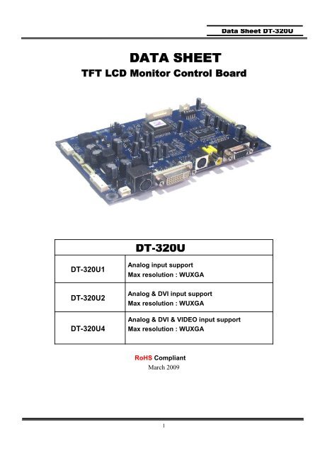
DATA SHEET TFT LCD Monitor Control Board DT-320U
DATA SHEET TFT LCD Monitor Control Board DT-320U
DATA SHEET TFT LCD Monitor Control Board DT-320U

Create successful ePaper yourself
Turn your PDF publications into a flip-book with our unique Google optimized e-Paper software.
<strong>DATA</strong> <strong>SHEET</strong><br />
<strong>TFT</strong> <strong>LCD</strong> <strong>Monitor</strong> <strong>Control</strong> <strong>Board</strong><br />
<strong>DT</strong>-<strong>320U</strong>1<br />
<strong>DT</strong>-<strong>320U</strong>2<br />
<strong>DT</strong>-<strong>320U</strong>4<br />
<strong>DT</strong>-<strong>320U</strong><br />
Analog input support<br />
Max resolution : WUXGA<br />
Analog & DVI input support<br />
Max resolution : WUXGA<br />
Analog & DVI & VIDEO input support<br />
Max resolution : WUXGA<br />
RoHS Compliant<br />
March 2009<br />
1<br />
Data Sheet <strong>DT</strong>-<strong>320U</strong>
CONTENT<br />
• INTRODUCTION --------------------------------------------- 4<br />
• GENERAL SPECIFICATION --------------------------------------------- 5<br />
• SYSTEM DESIGN --------------------------------------------- 8<br />
• BLOCK DIAGRAM --------------------------------------------- 9<br />
Data Sheet <strong>DT</strong>-<strong>320U</strong><br />
• ASSEMBLY NOTES --------------------------------------------- 10<br />
• CONNECTION & OPERATION --------------------------------------------- 13<br />
• OSD --------------------------------------------- 14<br />
• OSD FUNCTION --------------------------------------------- 15<br />
• CONNECTOR, PINOUT & JUMPER --------------------------------------------- 24<br />
• CONTROLLER DIMENSIONS --------------------------------------------- 36<br />
• APPLICATION NOTES ----------------------------------------- 37<br />
• TROUBLESHOOTING --------------------------------------------- 38<br />
• APPLICABLE GRAPHIC MODE --------------------------------------------- 39<br />
• ACCESSORY --------------------------------------------- 40<br />
• APPENDIX --------------------------------------------- 41<br />
2
Revision History<br />
Data Sheet <strong>DT</strong>-<strong>320U</strong><br />
No Data Revision Page<br />
1 Preliminary Release AA<br />
3
INTRODUCTION<br />
Data Sheet <strong>DT</strong>-<strong>320U</strong><br />
Designed for <strong>LCD</strong> monitor and other flat panel display application the <strong>DT</strong>-<strong>320U</strong> controller<br />
provides an auto-input synchronization and easy to sue interface controller for:<br />
► <strong>TFT</strong> (active matrix) <strong>LCD</strong> panels of 1024x768, 1280x768, 1366x768, 1280x1024, 1440x900,<br />
1680x1050, 1600x1200, 1920x1080 and 1920x1200 resolutions<br />
► Computer video signals of VGA, SVGA, XGA, WXGA, SXGA, WXGA+, WSXGA+, UXGA, FHD<br />
and WUXGA standard.<br />
► CVBS and SVHS Video signals of NTSC, PAL standard<br />
► 3-D Comb filter and Noise Reduction adoption<br />
► Input Signal Support<br />
� All VESA standard<br />
HOW TO PROCEED<br />
► Ensure that you have all parts & they are correct, refer to:<br />
� Connection diagram<br />
� Connector reference<br />
� Assembly notes<br />
► Check controller switch & jumper settings (Errors may damage the panel)<br />
► Prepare the PC & Video<br />
► Connect the parts<br />
► Understand the operation & functions<br />
IMPORTANT USAGE NOTE<br />
This equipment is for use by developers and integrators. The manufacturer accepts no liability for<br />
damage or injury caused by the use of this product. It is the responsibility of the developer,<br />
integrators or other users of this product to:<br />
� Ensure that all necessary and appropriate safety measures are taken.<br />
� Obtain suitable regulatory approvals as may be required.<br />
� Check power settings to all component parts before connection.<br />
DISCLAIMER<br />
There is no implied or expressed warranty regarding this material.<br />
4
GENERAL SPECIFICATION<br />
No. Item Description<br />
1 Model name<br />
2 <strong>LCD</strong> Module<br />
Data Sheet <strong>DT</strong>-<strong>320U</strong><br />
XGA Panel 1024X768 <strong>DT</strong>-320X4 Note 1)<br />
WXGA Panel 1280X768 <strong>DT</strong>-320W4<br />
WXGA Panel 1366X768 <strong>DT</strong>-320WZ4<br />
SXGA Panel 1280X1024 <strong>DT</strong>-320E4<br />
WXGA+ Panel 1440X900 <strong>DT</strong>-320WX4<br />
WSXGA+ Panel 1680X1050 <strong>DT</strong>-320WE4<br />
UXGA Panel 1600X1200 <strong>DT</strong>-<strong>320U</strong>4<br />
HD Panel 1920X1080 <strong>DT</strong>-320WH4<br />
WUXGA Panel 1920X1200 <strong>DT</strong>-320WU4<br />
XGA, WXGA, SXGA, WXGA+, WSXGA+, UXGA, HD,<br />
WUXGA<br />
3 Signal Input Analog RGB. TMDS(DVI-D). NTSC/PAL<br />
4<br />
5<br />
Resolution<br />
Support<br />
H: 31 ∼ 80kHz<br />
V: 55 ∼ 76Hz<br />
OSD <strong>Control</strong> Menu, Left, Right, Up, Down, Source, Power 5 keys<br />
Plug & Play VESA DDC 2B Ver1.3<br />
6 Power Connector Input<br />
7.<br />
Power<br />
Consumption<br />
8 Signal Connector<br />
Supply<br />
Voltage<br />
Type: IEC320 MALE 3Line<br />
Connector<br />
12Vdc/15Vdc/18Vdc or 24Vdc<br />
Max Power TBD<br />
Analog<br />
Notes 1) Depends On Panel Resolution<br />
- X : XGA (1024X768)<br />
- W : WXGA (1280X768)<br />
- WZ : WXGA (1366X768)<br />
- E : SXGA (1280X1024)<br />
- WX : WXGA+ (1440x900)<br />
- WE : WSXGA+ (1680x1050)<br />
- U : UXGA (1600x1200)<br />
- WH : FHD 1080i (1920x1080)<br />
- WU : WUXGA (1920x1200)<br />
DSUB 15P(R, G, B Separate H, V<br />
Sync)<br />
Digital DVI-D(TMDS) TMDS<br />
Video MINIDIN-4P(SVHS), RCA(CVBS)<br />
5
ELECTRICAL SPECIFICATION<br />
Input characteristic<br />
Data Sheet <strong>DT</strong>-<strong>320U</strong><br />
Description Signal Unit Min Typical Max Remarks<br />
Power In (24V)<br />
Power In (18V)<br />
Power In (15V)<br />
Power In (12V)<br />
RGB Input<br />
DVI Input<br />
NTSC/PAL<br />
Input Vdc 22.8 24.0 25.2<br />
Consumption Watt TBD Without INV<br />
Input Vdc 17.0 18.0 19.0<br />
Consumption Watt TBD Without INV<br />
Input Vdc 14.75 15.0 15.75<br />
Consumption Watt TBD Without INV<br />
Input Vdc 11.4 12.0 12.6<br />
Consumption Watt TBD Without INV<br />
Analog RGB Vp-p 0 0.7 -<br />
Sync Vdc 0 5.0 5.5<br />
H Frequency KHz 31 64 80 Depends on Mode<br />
V Frequency Hz 55 60 75<br />
TMDS mVp-p 450 500 900<br />
Y/CVBS Vp-p 0.7 1.0 1.4<br />
C Vp-p 0.6 0.8 1.0<br />
6
Output Characteristics<br />
Data Sheet <strong>DT</strong>-<strong>320U</strong><br />
Description Signal Unit Min Typical Max Remarks<br />
Panel Power<br />
LVDS Interface<br />
Inverter Interface<br />
<strong>LCD</strong> Power<br />
(18V)<br />
<strong>LCD</strong> Power<br />
(15V)<br />
<strong>LCD</strong> Power<br />
(12V)<br />
<strong>LCD</strong><br />
Power(5V)<br />
<strong>LCD</strong><br />
Power(3.3V)<br />
Differential<br />
output<br />
Vdc 17.1 18.0 18.9 Jumper option<br />
Vdc 14.25 15.0 15.75<br />
Vdc 11.4 12.0 12.6<br />
(Representative<br />
12V)<br />
Vdc 4.75 5.0 5.25 Jumper option<br />
Vdc 3.13 3.3 3.46 Jumper option<br />
Vp-p<br />
(mV)<br />
250 350 450 Different +/-<br />
Power out Vdc 22.8 24.0 25.2 Depends on Power<br />
On/Off<br />
control<br />
Brightness<br />
control<br />
17.1 18.0 18.9<br />
14.25 15.0 15.75<br />
11.4 12.0 12.6<br />
Input and Spec.<br />
V 0 3.3 L=off, H=on<br />
V 3.3 0 Option<br />
0 3.3 Option<br />
Step 0 100 OSD Value<br />
7
SYSTEM DESIGN<br />
Data Sheet <strong>DT</strong>-<strong>320U</strong><br />
A typical <strong>LCD</strong> based display system utilizing this controller is likely to comprise the following.<br />
J18<br />
J10<br />
J16<br />
CN104<br />
1. <strong>LCD</strong> PANEL<br />
J19: Jumper for <strong>LCD</strong> Power<br />
J13 Internal SMPS<br />
2. INVERTER<br />
6. INVERTER CABLE<br />
J25 Power Selection J5: Jumper for Panel Type.<br />
J26 Jumper for Inverter dimming<br />
J14 Jumper for Inverter Power 24V or 12V/15V/18V<br />
J23 Jumper for Output Power<br />
J101<br />
J7/J15 J17<br />
J24<br />
10. OUTPUT POWER<br />
5. OSD KEY CABLE<br />
4. OSD <strong>Board</strong><br />
3. <strong>LCD</strong> controller board<br />
J9 J4<br />
7. <strong>LCD</strong> INTERFACE CABLE<br />
J27 :<br />
J12 : RS232 / Debug<br />
J11<br />
J20 /J21<br />
J22 J3 J1 J8 J6 J2<br />
12. DC Power Jack (24V)<br />
13. DVI-D Input<br />
14. S-VIDEO Input<br />
8<br />
15. Composite Input<br />
11. RGB Input<br />
12. DC Power Jack (12V/15V/18V)
BLOCK DIAGRAM<br />
TMDS<br />
(DVI-D)<br />
RED<br />
GREEN<br />
BLUE<br />
SYNC<br />
(DSUB<br />
15P)<br />
CVBS(RCA)<br />
SVHS(MD 4P)<br />
POWE<br />
VIDEO DECODER<br />
(TVP5160)<br />
E 2 PROM<br />
DC/DC<br />
SCALER<br />
(RTD2553V)<br />
Power <strong>Control</strong><br />
9<br />
MCU<br />
(MTV412)<br />
Data Sheet <strong>DT</strong>-<strong>320U</strong><br />
LVDS 2ch<br />
Inverter
ASSEMBLY NOTES<br />
Data Sheet <strong>DT</strong>-<strong>320U</strong><br />
This controller is designed for monitors and custom display projects using <strong>TFT</strong> (active matrix) <strong>LCD</strong><br />
panels of 1024x768, 1280x768, 1366x768, 1280x1024, 1440x900, 1680x1050, 1600x1200,<br />
1920x1080 and 1920x1200 resolutions,<br />
Preparation: Before proceeding it is important to familiarize yourself with the parts making up the<br />
system and the various connectors, mounting holes and general layout of the controller. As much<br />
as possible connectors have been labeled. Guides to connectors and mounting holes are shown in<br />
the following relevant sections.<br />
1. <strong>LCD</strong> Panel: This controller has LVDS interface logic on the <strong>Board</strong> for different kind of <strong>TFT</strong> <strong>LCD</strong><br />
panel. Due to the different signal timing and electrical characteristics from each <strong>LCD</strong> panel<br />
manufacturer, for selecting <strong>LCD</strong> interface type and resolution, put jumper marked J5 on the right<br />
position following <strong>LCD</strong> panel specification. For selecting DC power level, put jumper marked J19<br />
on the right position. Supplied power level depends on <strong>LCD</strong> panel specification.<br />
2. <strong>Control</strong>ler: Handle the controller with care as static charge may damage electronic components,<br />
Make sure correct jumper and switches settings to match the target <strong>LCD</strong> panel<br />
3. <strong>LCD</strong> connector board: Different makers and models of <strong>LCD</strong> panel require different panel signal<br />
connectors and different pin assignments.<br />
4. <strong>LCD</strong> signal cables: In order provide a clean signal it is recommended that <strong>LCD</strong> signal cables<br />
should not longer than 30cm. If loose wire cabling is utilized these can be a made into a harness<br />
with cable ties. Care should be taken when you place the cables to avoid signal interface.<br />
Additionally it may necessary in some systems to add ferrite cores to the cables to minimize<br />
signal noise.<br />
5. Inverter: This will be required for the backlight of an <strong>LCD</strong>, some <strong>LCD</strong> panel have an inverter<br />
built in. As <strong>LCD</strong> panels may have 1 or more backlight tubes and the power requirements for<br />
different panel backlights may vary it is important to match the inverter in order to obtain<br />
optimum performance. See application notes for more information on connection.<br />
6. Inverter cable: Different inverter models require different cables and different pin assignment.<br />
Make sure the correct cable pin out to match the inverter. Unsuitable cable pins out may<br />
damage the inverter.<br />
7. AV cable: Standard composite or S-video cables can be used. Reasonable quality cables<br />
should be used to avoid image quality degradation.<br />
8. OSD Button: See Operational Function section.<br />
10
9. 3 Color LED: This LED shows the state of controller.<br />
� Green –Normal state<br />
� Red – Of mode (Can’t find video signals)<br />
� Amber –DPMS mode<br />
10. Power switch: This switch is located on OSD button board.<br />
Data Sheet <strong>DT</strong>-<strong>320U</strong><br />
11. Power input: Proper power is required to supply power for the controller, the Inverter and the<br />
<strong>LCD</strong> panel<br />
12. VGA Input Cable: As this may affect regulatory emission test result, a suitably shielded cable<br />
should be utilized.<br />
EMI: Shielding will be required for passing certain regulatory emissions tests. Also the choice of<br />
video board and power supply can affect the test result.<br />
Consideration should be given to:<br />
� Electrical insulation.<br />
� Grounding.<br />
� EMI shielding.<br />
� Heat & ventilation<br />
Caution: Ensure that the adequate insulation is provided for all areas of the PCB with special<br />
attention to high voltage parts such as the inverter.<br />
*** Remarks***<br />
For a specific panel use, One <strong>LCD</strong> panel sample and full technical specifications for the <strong>LCD</strong><br />
panel from the manufacturer are required to test for tuning up screen image.<br />
Kordis can provide engineering service for customers specific controller development.<br />
Please contact Kordis . (dyoh@kordis.co.kr )<br />
13. Setup for operation<br />
Once the circuit has been connected, a setup procedure for optimal is requires a few minutes<br />
The following instructions are likely to form the basis of the finished product operation<br />
manual.<br />
PC Settings<br />
The PC needs to be set to an appropriate graphics mode that has the same resolution with the<br />
<strong>LCD</strong> panel to have clear screen image. And the vertical refresh rate should be set to one of<br />
56~75Hz, non –interlaced signal.<br />
11
<strong>LCD</strong> display System Settings<br />
Data Sheet <strong>DT</strong>-<strong>320U</strong><br />
The OSD (On Screen Display) provides certain functions to have clear image and others. This<br />
board supports 5 buttons OSD operation as a standard. The control functions defined on OSD<br />
operation are as below.<br />
Pc Graphics Output: A few guidelines:<br />
� Signal quality is very important, if there is noise or instability in the PC graphics output<br />
this may result in visible noise on the display<br />
� Refer to the graphic modes table in specification section for supported modes.<br />
� Non-interlaced & interlaced video input is acceptable.<br />
Important: please read the application notes section for more information.<br />
12
CONNECTION & OPERATION<br />
Data Sheet <strong>DT</strong>-<strong>320U</strong><br />
CAUTION: Never connect or disconnect parts of the display system when the system is powered<br />
CONNECTION<br />
up as this may cause serious damage.<br />
1. <strong>LCD</strong> panel & Inverter: Connect the inverter (if it is not built- in the panel) to the CCFT lead<br />
connector of the <strong>LCD</strong> panel.<br />
2. LVDS type panels: Plug the signal cables direct to J11 of the controller board for Single<br />
Channel interface resolution Panel or for dual channel interface panel. Plug the other end of<br />
cables to the <strong>LCD</strong> connector board.<br />
3. Inverter & <strong>Control</strong>ler: Plug the inverter cable to J10/J16 of the controller board and<br />
another end to the connector on the inverter. Make sure J14 jumper position for Inverter<br />
Power<br />
4. Function switch & <strong>Control</strong>ler: Plug the OSD switch mount cable to CN104 of the<br />
controller board and another end to the OSD board.<br />
5. Jumpers & Switch: Check all jumpers J23 (External power Setting), J19 (Target panel<br />
power is setting), J5 (Target Panel Option switch) and J14 (Inverter Power) are set correctly.<br />
Details referring the jumpers and switches setting table (in the following section)<br />
6. VGA cable & <strong>Control</strong>ler: Plug the VGA cable to the connector J6/J4 of the controller board.<br />
7. DIV-D Cable & <strong>Control</strong>ler: Plug the DVI-D Cable to the connector J3/J101 of the controller<br />
board.<br />
8. C/S-Video Cable & <strong>Control</strong>ler: Plug S-Video Cable to the connector J1/J7, C-Video Cable<br />
to the J8/J9<br />
9. Power supply & <strong>Control</strong>ler: Plug the DC 12V/15V/18V power in to the connector J2/J20<br />
and DC 24V power in to the connector J22/J7 of controller board.<br />
10.SMPS & <strong>Control</strong>ler : Plug the SMPS power in to the connector J13 of controller board<br />
11.Power on: Switch on the controller board and panel by using the OSD switch mount.<br />
General:<br />
� If you use supplied cables & accessories, ensure that they are correct for the model of the<br />
panel and the controller.<br />
� If you make your own cables & connectors, refer carefully to both the panel & inverter<br />
specifications and the section in this manual, “Connectors,Pin outs & Jumpers”to ensure<br />
the correct pin to pin wiring.<br />
PC Setting:<br />
The controller has been designed to take a very wide range of input signals however to<br />
optimize the PC’sgraphic performance we recommend choosing 60Hz vertical refresh rate –<br />
this will not cause screen flicker.<br />
13
OSD <strong>Control</strong> <strong>Board</strong><br />
Data Sheet <strong>DT</strong>-<strong>320U</strong><br />
The OSD (On Screen Display) provides certain functions to have clear image and others. This<br />
board supports 5 buttons OSD operation as a standard. The control functions defined on OSD<br />
operation are as below. (unit: mm)<br />
Appearance<br />
1.6<br />
7.5<br />
MENU<br />
SEL<br />
AUTO DOWN UP LED<br />
Source change<br />
POWER<br />
ON/OFF<br />
Button Function Status HOT Key<br />
Power Power on/off On/Off<br />
Menu Activate menu<br />
Select Menu Select No OSD Auto Adjust<br />
LED Indicates operation status Green/ Red/ Amber<br />
DOWN, UP Cursor control(Value <strong>Control</strong>)<br />
Down(Decrement)/Up(Increment)<br />
14<br />
3.0<br />
UP : Source change
Data Sheet <strong>DT</strong>-<strong>320U</strong><br />
The chosen OSD settings will be stored in memory. The OSD menu can be cleared from the<br />
screen from the screen by moving the selection bar to the EXIT MENU icon pressing the SEL<br />
button otherwise it will be automatically cleared after a few second of non-use<br />
OSD MAIN MENU<br />
VIDEO MODE RGB MODE DVI MODE<br />
P i c t u r e P i c t u r e P i c t u r e<br />
P S M C S M C S M<br />
B r i g h t n e s s B r i g h t n e s s B r i g h t n e s s<br />
C o n t r a s t C o n t r a s t C o n t r a s t<br />
C o l o r<br />
S h a r p n e s s<br />
T i n t<br />
E x i t : M E N U ◀▶▲▼ E x i t : M E N U ◀▶▲▼ E x i t : M E N U ◀▶▲▼<br />
S e t u p S e t u p S e t u p<br />
L a n g u a g e L a n g u a g e L a n g u a g e<br />
T r a n s p a r e n c y T r a n s p a r e n c y T r a n s p a r e n c y<br />
A s p e c t A s p e c t A s p e c t<br />
S e t I D S e t I D S e t I D<br />
V o l u me V o l u me V o l u me<br />
F a c t o r y r e s e t F a c t o r y r e s e t F a c t o r y r e s e t<br />
E x i t : M E N U ◀▶▲▼ E x i t : M E N U ◀▶▲▼ E x i t : M E N U ◀▶▲▼<br />
S c r e e n<br />
A u t o c o n f i g u r e<br />
H - P o s i t i o n<br />
V - P o s i t i o n<br />
C l o c k<br />
P h a s e<br />
XGA Mode<br />
E x i t : M E N U ◀▶▲<br />
▼<br />
15
Picture<br />
VIDEO MODE<br />
RGB MODE<br />
16<br />
Data Sheet <strong>DT</strong>-<strong>320U</strong>
Brightness / Contrast / Color / Sharpness<br />
Tint<br />
17<br />
Data Sheet <strong>DT</strong>-<strong>320U</strong>
Setup<br />
Language<br />
Transparency<br />
18<br />
Data Sheet <strong>DT</strong>-<strong>320U</strong>
Aspect<br />
Set ID<br />
Volume<br />
19<br />
Data Sheet <strong>DT</strong>-<strong>320U</strong>
Factory Reset<br />
Screen<br />
PICTURE<br />
ICON<br />
S c r e e n<br />
PIP<br />
ICON<br />
PICTURE PIP<br />
ICON ICON<br />
S c r e e n<br />
SETUP<br />
ICON<br />
A u t o c o n f i g u r e<br />
H p o s i t i o n<br />
V p o s i t i o n<br />
C l o c k<br />
P h a s e<br />
XGA Mode<br />
E x i t : M E N U ◀▶▲<br />
▼<br />
Auto Configure<br />
SETUP<br />
ICON<br />
Data Sheet <strong>DT</strong>-<strong>320U</strong><br />
A u t o c o n f i g u r e ▶ T o s e t<br />
H p o s i t i o n 5 0<br />
V p o s i t i o n 5 0<br />
C l o c k 5 0<br />
P h a s e 5 0<br />
XGA Mode<br />
E x i t : M E N U ◀▶▲<br />
▼<br />
20
H Position / V Position / Clock / Phase<br />
PICTURE<br />
ICON<br />
S c r e e n<br />
PIP<br />
ICON<br />
SETUP<br />
ICON<br />
Data Sheet <strong>DT</strong>-<strong>320U</strong><br />
A u t o c o n f i g u r e ▶<br />
H p o s i t i o n 5 0<br />
V p o s i t i o n 5 0<br />
C l o c k 5 0<br />
P h a s e 5 0<br />
XGA Mode AUTO<br />
E x i t : M E N U ◀▶▲<br />
▼<br />
XGA Mode<br />
* XGA Mode : Setting of Auto configuration for XGA up to WXGA at Analog input<br />
21
OSD GUI <strong>Control</strong> Table<br />
MAIN MENU SUB MENU CONTROL<br />
PICTURE<br />
PSM<br />
CSM<br />
Dynamic/Standard/Mild/Game/User<br />
USER Brightness, Contrast, Color, Sharpness<br />
CSM/Brightness/Contrast<br />
CSM 5800K/9300K/6500K/User<br />
User Red/Green/Blue<br />
Language English/Deutsch/Français/Italiano/Espanol<br />
SETUP Transparency 50 (1 ~100)<br />
SCREEN<br />
Factory Reset On/Off<br />
Auto Configure On/Off<br />
H Position 50( 0 ~ 100)<br />
V Position 50( 0 ~ 100)<br />
Clock 50( 0 ~ 100)<br />
Phase 50( 0 ~ 100)<br />
XGA Mode AUTO / 1366*768 / 1280*768 / 1024*768<br />
* XGA Mode : Setting of Auto configuration for XGA up to WXGA at Analog input<br />
22<br />
Data Sheet <strong>DT</strong>-<strong>320U</strong><br />
VIDEO<br />
PC<br />
RGB PC
Operation Message<br />
OUT OF FREQUENCY<br />
Input Signal is over the supporting range<br />
POWER SAVER MODE<br />
Input Signal is not present. This message is<br />
disappeared after 5 seconds.<br />
SELF DIAGNOSTICS<br />
Input Signal is not present after power on<br />
with power switch. This message is not<br />
disappeared before power off or activity of<br />
input signal.<br />
AUTO CONFIGURATION<br />
Execute AUTO Function.<br />
23<br />
Data Sheet <strong>DT</strong>-<strong>320U</strong>
CONNECTOR, PINOUT & JUMPERS<br />
The various connectors are:<br />
J18<br />
CN104<br />
J10<br />
J16<br />
Summary<br />
J14<br />
J23<br />
J24<br />
J19<br />
J25<br />
J26<br />
J7 / J15<br />
J3<br />
J101<br />
J13<br />
J1<br />
J22 J8<br />
J17 J9 J6<br />
J5<br />
J12<br />
J27<br />
J4<br />
Data Sheet <strong>DT</strong>-<strong>320U</strong><br />
Reference Item Description Type Manufacture<br />
J1 Jack S-video Input MJ373 MINIDIN 4PIN<br />
J2 Jack 12V Input Dc power 2.5Ø -<br />
J3 Connector DVI-D Input(TMDS) DVI-D 24P<br />
J4 Wafer Analog RGB Input 20017WR-1210 YEONHO<br />
J5 Switch Panel Type Selection HDR5X2 -<br />
J6 Connector Analog RGB Input 15P D-SUB -<br />
J7 Wafer 24V Power Input 20017WR-0410 YEONHO<br />
J8 Jack C-video Input RCA(Yellow) -<br />
J9 Wafer C-video Input 20017WR-0310 YEONHO<br />
J10, J16 Wafer Inverter Interface 12505WR-1090 YEONHO<br />
J11 Wafer LVDS Interface 12507WR-30 YEONHO<br />
J12 Wafer To RS232 or Debugger SMW200-0410 YEONHO<br />
J13 Wafer Internal SMPS Power Input SMW200-1410 YEONHO<br />
J14 Jumper Inverter Power Selection HDR3X1<br />
J15 Block 24V Input Terminal Block BR-500C<br />
J17 Wafer S-Video Input 20017WR-0510 YEONHO<br />
J18 Wafer 24V Power Input 20017WR-0910 YEONHO<br />
J19 Jumper Panel Power Selection HDR2X4<br />
J20 Wafer 12V Power Input 20017WR-0410 YEONHO<br />
24<br />
J2<br />
J11<br />
J20<br />
J21
Data Sheet <strong>DT</strong>-<strong>320U</strong><br />
Reference Item Description Type Manufacture<br />
J21 Block 12V Input Terminal Block BR-500C<br />
J22 Jack 24V Input Dc power KPJ-4S-S KYCON<br />
J23 Jumper Output Power Selection HDR3X1<br />
J24 Wafer Output Power 20017WR-0310 YEONHO<br />
J25 Jumper 5V Power Selection HDR3X1<br />
J26 Jumper Inverter Dimming Selection HDR3X1<br />
J27 Wafer External (YPbPr, Audio<br />
<strong>Board</strong>)<br />
SMW200-1210 YEONHO<br />
J101 Wafer DVI-D Input 12507WR-20 YEONHO<br />
CN104 Wafer To OSD <strong>Board</strong> 20017WR-0710 YEONHO<br />
J1: S-Video Input Jack<br />
Pin No. Symbol Description<br />
1 GND Ground<br />
2 GND Ground<br />
3 C-in CROMA signal input<br />
4 Y-in LUMA signal input<br />
5 GND Ground<br />
6 GND Ground<br />
7 GND Ground<br />
J2: 12V DC power supply Jack<br />
Pin No. Symbol Description Pin No. Symbol Description<br />
Center Vcc 12V Shell GND Ground<br />
J3: DVI-D Input Connector<br />
Pin No. Symbol Description<br />
1 TMDS <strong>DATA</strong>2- TMDS <strong>DATA</strong>2 Differential Negative Signal<br />
2 TMDS <strong>DATA</strong>2+ TMDS <strong>DATA</strong>2 Differential Positive Signal<br />
3 TMDS <strong>DATA</strong>2 Shield Shield for TMDS Channel #2<br />
4 NC No Connection<br />
5 NC No Connection<br />
6 SDA The Data Line for the DDC Interface<br />
25
Data Sheet <strong>DT</strong>-<strong>320U</strong><br />
7 SCL The Clock Line for the DDC Interface<br />
8 NC No Connection<br />
9 TMDS <strong>DATA</strong>1- TMDS <strong>DATA</strong>1 Differential Negative Signal<br />
10 TMDS <strong>DATA</strong>1+ TMDS <strong>DATA</strong>1 Differential Positive Signal<br />
11 TMDS <strong>DATA</strong>1 Shield Shield for TMDS Channel #1<br />
12 NC No Connection<br />
13 NC No Connection<br />
14 +5V Power +5 Volt signal for EDID (Un-powered <strong>Monitor</strong>)<br />
15 GND(for +5V) Ground for +5 Volt Power pin, Sync return<br />
16 HPD Identify the presence of a monitor<br />
17 TMDS <strong>DATA</strong>0- TMDS <strong>DATA</strong>0 Differential Negative Signal<br />
18 TMDS <strong>DATA</strong>0+ TMDS <strong>DATA</strong>0 Differential Positive Signal<br />
19 TMDS <strong>DATA</strong>0 Shield Shield for TMDS Channel #0<br />
20 NC No Connection<br />
21 NC No Connection<br />
22 TMDS CLOCK Shield Shield for TMDS Clock differential Pair<br />
23 TMDS CLOCK+ TMDS <strong>DATA</strong>0 Differential Positive Signal<br />
24 TMDS CLOCK- TMDS <strong>DATA</strong>0 Differential Negative Signal<br />
J4: Analog RGB Input Wafer<br />
Pin No. Symbol Description<br />
1 SCL Serial Clock Line for DDC<br />
2 SDA Serial Data Line for DDC<br />
3 NC No Connection<br />
4 VSYNC Vertical Sync<br />
5 HSYNC Horizontal Sync<br />
6 GND Ground for HSYNC, VSNC, SCL, SDA<br />
7 BLUE BLUE analog input<br />
8 BLUE GND Ground for BLUE Input Signal<br />
9 GREEN GREEN analog input<br />
10 GREEN GND Ground for GREEN Input Signal<br />
11 RED RED analog input<br />
12 RED GND Ground for RED Input Signal<br />
26
J5: Panel Type Selection Switch<br />
* See the appendix more information –41 Page<br />
J6: Analog RGB Input Connector<br />
Pin No. Symbol Description<br />
1 Red1 Red analog input<br />
2 Green1 Green analog input<br />
3 Blue1 Blue analog input<br />
4 GND Ground<br />
5 GND Ground<br />
6 GND Ground<br />
7 GND Ground<br />
8 GND Ground<br />
9 NC Not connected<br />
10 GND Ground<br />
11 GND Ground<br />
12 DSDA DDC-SDA<br />
13 HSYNC Horizontal Sync<br />
14 VSYNC Vertical Sync<br />
15 DSCL Serial Clock Input<br />
J7: 24V DC power Input Wafer<br />
Pin No. Symbol Description<br />
1,2 Vcc 24V<br />
3,4 GND Ground<br />
J8: C-video Input Jack<br />
Data Sheet <strong>DT</strong>-<strong>320U</strong><br />
Pin No. Symbol Description Pin No. Symbol Description<br />
1,2 CVBS Composite-video input 3 GND Ground<br />
J9: C-video Input Wafer<br />
Pin No. Symbol Description<br />
1,3 Composite CVBS input signal<br />
2 GND Ground<br />
27
J11: <strong>LCD</strong> Interface Wafer for 2 Ch LVDS Type<br />
Pin No. Symbol Description<br />
1 MOD_PWR Panel Power (12V/18V, 5V or 3.3V)<br />
2 MOD_PWR Panel Power (12V/18V, 5V or 3.3V)<br />
3 MOD_PWR Panel Power (12V/18V, 5V or 3.3V)<br />
4 MOD_PWR Panel Power (12V/18V, 5V or 3.3V)<br />
5 GND Ground<br />
Data Sheet <strong>DT</strong>-<strong>320U</strong><br />
6 SELLDS LVDS <strong>DATA</strong> ORDER SELECT(Depends on Panel)/ No Connection<br />
7 GND Ground<br />
8 Y3P-EVEN Positive(+) LVDS differential first 3 data(B port)<br />
9 Y3M-EVEN Negative(-) LVDS differential first 3 data(B port)<br />
10 YCP-EVEN Positive(+) LVDS differential first Clock(B port)<br />
11 YCM-EVEN Negative(-) LVDS differential first Clock(B port)<br />
12 Y2P-EVEN Positive(+) LVDS differential first 2 data(B port)<br />
13 Y2M-EVEN Negative(-) LVDS differential first 2 data(B port)<br />
14 GND Ground<br />
15 Y1P-EVEN Positive(+) LVDS differential first 1 data(B port)<br />
16 Y1M-EVEN Negative(-) LVDS differential first 1 data(B port)<br />
17 YOP-EVEN Positive(+) LVDS differential first 0 data(B port)<br />
18 Y0M-EVEN Negative(-) LVDS differential first 0 data(B port)<br />
19 GND Ground<br />
20 Y3P-ODD Positive(+) LVDS differential second 3 data(A port)<br />
21 Y3M-ODD Negative(-) LVDS differential second 3 data(A port)<br />
22 YCP-ODD Positive(+) LVDS differential second Clock(A port)<br />
23 YCM-ODD Negative(-) LVDS differential second Clock(A port)<br />
24 Y2P-ODD Positive(+) LVDS differential second 2 data(A port)<br />
25 Y2M-ODD Negative(-) LVDS differential second 2 data(A port)<br />
26 GND Ground<br />
27 Y1P-ODD Positive(+) LVDS differential second 1 data(A port)<br />
28 Y1M-ODD Negative(-) LVDS differential second 1 data(A port)<br />
29 YOP-ODD Positive(+) LVDS differential second 0 data(A port)<br />
30 Y0M-ODD Negative(-) LVDS differential second 0 data(A port)<br />
28
J10, J16: Backlight Inverter Interface Wafer<br />
Pin No. Symbol Description<br />
Data Sheet <strong>DT</strong>-<strong>320U</strong><br />
1 DIM-ADJ DIM-adjustment analog dimming control signal<br />
* make sure inverter specification<br />
2 ON/OFF Inverter digital ON(3.3V) / OFF(0V) signal<br />
3,4,5,6 GND Ground<br />
7,8,9,10 Vcc B+(24V or 12/18V)<br />
J12: To RS232 or Debugger Interface Wafer<br />
Pin No. Symbol Description<br />
1 SCL/RXD I2C_SCL_ISP / UART_RX<br />
2 SDA/TXD I2C_SDA_ISP / UART_TX<br />
3 GND Ground<br />
4 5VS +5V<br />
J13: Internal SMPS Input Power Supply Wafer<br />
Pin No. Symbol Description I/O Remarks<br />
1 NC No Connection<br />
2 GND Ground<br />
3,4 12V 12V Logic Power Supply I Max 1.0A<br />
5,6 GND Ground<br />
7,8 5VP 5V Logic Power Supply I Max 1.0A<br />
9 5VS 5V Standby Power Supply I<br />
10,11 GND Ground<br />
12 PWR_ON SMPS Power On <strong>Control</strong> Signal O 3.3V(High):On,<br />
13 INV_DIM Inverter Dimming <strong>Control</strong> Signal O<br />
14 INV_CTRL Inverter ON/OFF <strong>Control</strong> Signal O<br />
J14 : For Inverter power(12V/24V) Selection Jumper<br />
Pin No. Symbol Description<br />
0.7V:OFF<br />
1 12V representative 12V/15V/18V, depends on power supply from J2<br />
2 B+ Inverter power selected by J14’Jumper<br />
3 24V 24V from J22<br />
29
J15: +24V Power Input Terminal Block<br />
Pin No. Symbol Description<br />
1 24V 24V<br />
2 GND Ground<br />
J17: S-Video Input Wafer<br />
Pin No. Symbol Description<br />
1,2 C-in CROMA signal input<br />
3 GND Ground<br />
4,5 Y-in LUMA signal input<br />
J18 : 24V Power Input Wafer<br />
Pin No. Symbol Description<br />
1,2,3,4 GND Ground<br />
5,6,7,8,9 Vcc 24V<br />
J19 : Panel Power Selection Jumper<br />
* See the Summary: jumpers setting more information –35 Page<br />
J20: 12V Power Input Wafer<br />
Pin No. Symbol Description<br />
1,2 Vcc 12V<br />
3,4 GND Ground<br />
J21: +12V Power Input Terminal Block<br />
Pin No. Symbol Description<br />
1 12V 12V<br />
2 GND Ground<br />
J22: 24V Input Dc power Jack<br />
Pin No. Symbol Description<br />
1,3 GND Ground<br />
2,4 Vcc 24V<br />
1 2<br />
3 4<br />
Data Sheet <strong>DT</strong>-<strong>320U</strong><br />
EX) LSE0227B24130(4PIN) Li-shin Adapter / SLS0227B24118<br />
30
J23: Output Power Selection Jumper<br />
Pin No. Symbol Description<br />
1 12V 12V<br />
2 Vcc On board power enable<br />
3 5V 5V<br />
J24: Out Power Wafer<br />
Pin No. Symbol Description<br />
1 Vcc 12V/5V from selected J23<br />
2 GND Ground<br />
3 GND Ground<br />
J25 : 5V Power Selection Jumper<br />
* See the Summary: jumpers setting more information –33 Page<br />
J26 : Inverter Dimming Selection jumper<br />
* See the Summary: jumpers setting more information –34 Page<br />
J27: External (YPbPr, Audio <strong>Board</strong>) Wafer<br />
Pin No. Symbol Description<br />
1 VOLUME Volume for Audio amp.<br />
2 MUTE Mute for Audio amp.<br />
3 GND Ground<br />
4 Pb/B Pb or BLUE<br />
5 GND Ground<br />
6 Y/G Y or GREEN<br />
7 GND Ground<br />
8 Pr/R Pr or RED<br />
9 GND Ground<br />
10 GND Ground<br />
11 12V 12V Power for Audio amp.<br />
12 12V 12V Power for Audio amp.<br />
31<br />
Data Sheet <strong>DT</strong>-<strong>320U</strong>
J101 : DVI-D Input Wafer<br />
Pin No. Symbol Description<br />
1 GND GROUND<br />
2 HPD Hot Plug Detect<br />
Data Sheet <strong>DT</strong>-<strong>320U</strong><br />
3 TMDS <strong>DATA</strong>2+ TMDS <strong>DATA</strong>2 Differential Positive Signal<br />
4 TMDS <strong>DATA</strong>2- TMDS <strong>DATA</strong>2 Differential Negative Signal<br />
5 GND GROUND<br />
6 TMDS <strong>DATA</strong>1+ TMDS <strong>DATA</strong>1 Differential Positive Signal<br />
7 TMDS <strong>DATA</strong>1- TMDS <strong>DATA</strong>1 Differential Negative Signal<br />
8 GND GROUND<br />
9 GND GROUND<br />
10 TMDS <strong>DATA</strong>0+ TMDS <strong>DATA</strong>0 Differential Positive Signal<br />
11 TMDS <strong>DATA</strong>0- TMDS <strong>DATA</strong>0 Differential Negative Signal<br />
12 GND GROUND<br />
13 TMDS CLOCK+ TMDS <strong>DATA</strong>0 Differential Positive Signal<br />
14 TMDS CLOCK- TMDS <strong>DATA</strong>0 Differential Negative Signal<br />
15 GND GROUND<br />
16 DDV5VD +5 Volt signal for EDID (Un-powered <strong>Monitor</strong>)<br />
17 NC No Connection<br />
18 SCL The Clock Line for the DDC Interface<br />
19 SDA The Data Line for the DDC Interface<br />
20 GND GROUND<br />
CN104: To OSD <strong>Board</strong> <strong>Control</strong> Wafer<br />
Pin No. Symbol Description<br />
1 Vcc +5V power for IR sensor<br />
2 IRQ Infrared rays signal line.<br />
3 LED2 RED LED<br />
4 LED1 GREEN LED<br />
5 GND Ground<br />
6 KEY1 Up, Power<br />
7 KEY0 Menu, Select, Down<br />
32
Summary : Jumpers Setting<br />
Reference Description Connector Type<br />
J14 +12/15/18V inverter<br />
power enable<br />
+24V inverter power<br />
enable<br />
J25 <strong>LCD</strong> External PSU Input<br />
<strong>LCD</strong> Internal SMPS Input<br />
33<br />
Data Sheet <strong>DT</strong>-<strong>320U</strong><br />
12V 24V<br />
12V 24V<br />
5VSA 5VSB<br />
5VSA 5VSB
Reference Description Connector Type<br />
J26 Inverter Brightness Max<br />
High<br />
Inverter Brightness Max<br />
Low<br />
J23 For External Power 12V<br />
For External Power 5V<br />
34<br />
Data Sheet <strong>DT</strong>-<strong>320U</strong><br />
DIMADJ1 DIMADJ2<br />
DIMADJ1 DIMADJ2<br />
12V 5V<br />
12V 5V
J19 5.0V panel power<br />
Only Internal SMPS<br />
(If Power come from J13)<br />
CAUTION: Incorrect<br />
setting can damage panel<br />
5.0V panel power<br />
Only PSU Input<br />
CAUTION: Incorrect<br />
setting can damage panel<br />
3.3V panel power<br />
Only PSU Input<br />
CAUTION: Incorrect<br />
setting can damage panel<br />
12V panel power<br />
- PSU & Internal SMPS<br />
CAUTION: Incorrect<br />
setting can damage panel<br />
* Power operation scheme :<br />
Data Sheet <strong>DT</strong>-<strong>320U</strong><br />
12V 3.3V 5VS 5VP<br />
12V 3.3V 5VS 5VP<br />
12V 3.3V 5VS 5VP<br />
12V 3.3V 5VS 5VP<br />
- 24V power supply from J22, 12V power generated by DC/DC converter so all 12V as marked 12V<br />
- 12V, 15V or 18V from J2, marked 12V is representative 12V, 15V or 18V as well as power supply<br />
35
CONTROLLER DIMENSIONS<br />
1.6T<br />
14.64mm<br />
36<br />
Data Sheet <strong>DT</strong>-<strong>320U</strong><br />
Max 3mm
APPLICATION NOTES<br />
USING THE CONTROLLER WITHOUT BOTTONS ATTACHED<br />
This is very straight forward:<br />
Data Sheet <strong>DT</strong>-<strong>320U</strong><br />
� Firstly setup the controller/display system with the buttons. With the attached controllers<br />
and display system active make any settings for color, contrast and image position as<br />
required then switch everything off.<br />
� Remove the control switches, the 7-way cable.<br />
� Refer to inverter specifications for details as to fixing brightness to a desired level, this may<br />
require a resistor, an open circuit or closed circuit depending on inverter<br />
INVERTER CONNECTION<br />
There are 3 potential issues to consider with inverter connection:<br />
� Power<br />
� ON/OFF<br />
� Brightness (DIM-ADJ)<br />
Inverter power: This should be matched with the inverter specification.<br />
Inverter ON/OFF: This is a pin provided on some inverter for ON/OFF function and is used by this<br />
panel controller for VESA DPMS compliance. If the inverter does not have on/off pin or the on/off<br />
pin is not used DPMS will not operate. Pin 5 should be matched to the inverter specification for the<br />
ON/OFF pin.<br />
Brightness Dimming control: <strong>DT</strong>-<strong>320U</strong> <strong>Control</strong>ler boards are analog dimming control method.<br />
And it is important to consider the specifications for the inverter to be used.<br />
37
TROUBLESHOOTING<br />
General<br />
Data Sheet <strong>DT</strong>-<strong>320U</strong><br />
A general guide to troubleshooting of a flat panel display system it worth considering the system as<br />
separate elements, such as:<br />
► <strong>Control</strong>ler (jumpers, PC settings)<br />
► Panel (controller, cabling, connection, panel, PC settings)<br />
► Backlight (inverter, cabling, connection, panel, Pc settings)<br />
► Cabling<br />
► Computer system (display settings, operating system)<br />
Through checking the system step by step cross with instruction manuals and a process of<br />
elimination to isolate the problem it is usually possible to clearly identify the problem area.<br />
No image:<br />
► If the panel backlight is not working it may still be possible to see just some image.<br />
► A lack of image is most likely to be caused by incorrect connection, lack of power, failure to<br />
provide a signal or incorrect graphic card settings.<br />
Image position:<br />
If it is impossible to position the image correctly, the image adjustment controls will not move the<br />
image far enough, then test using another graphics card. This situation can occur when a graphic<br />
card is not close to standard timing or when something is in the graphics line that may affect the<br />
signal such as a signal splitter (please note that normally a signal splitter will not have any adverse<br />
effect).<br />
Image appearance:<br />
► A faulty panel can have blank lines, failed sections, flickering or flashing display.<br />
► Incorrect graphic card refresh rate, resolution or interlaced mode will probably cause the image<br />
to be the wrong size, to scroll to, flicker badly or possibly even no image.<br />
► Incorrect jumper settings on the controller may cause everything from incorrect image viewing<br />
to total failure.<br />
CAUTION: Do not set the panel power input incorrectly.<br />
► Sparkling on the display: faulty panel signal cable.<br />
Backlight:<br />
Items to check include: Power input, controls, inverter and Tubes generally in this order.<br />
If half the screen is dimmer than the other half:<br />
► Check cabling for the inverter.<br />
Also:<br />
► If system does not power down when there is a loss of signal.<br />
38
APPLICABLE GRAPHIC MODE<br />
Data Sheet <strong>DT</strong>-<strong>320U</strong><br />
The microprocessor measures the, H –sync V –sync and polarity for RGB Inputs, and uses this<br />
timing information to control all of the display operation to get the proper image on a screen. This<br />
board can detect all VESA standard Graphic modes shown on the table below and Provide mare<br />
clear and stable image on a screen<br />
Table 6.1) RGB input format<br />
Spec Pixel Horizontal Timing Vertical Timing<br />
Mode<br />
Freq. Sync<br />
Polar<br />
Freq. Total Active Sy<br />
nc<br />
Po<br />
lar<br />
Freq. Total Active<br />
MHz KHz Pixel Pixel Hz Line Lind<br />
640*350@70Hz 25.144 P 31.430 800 640 N 70.000 449 350<br />
640*400@70Hz 28.287 N 31.430 800 640 P 70.000 449 400<br />
720*400@ 70Hz 28.287 N 31.430 900 720 P 70.000 449 400<br />
640*480@60Hz 28.175 N 31.469 800 640 N 59.940 525 480<br />
640*480@72Hz 31.500 N 37.861 832 640 N 72.809 520 480<br />
640*480@75Hz 31.500 N 37.500 840 640 N 75.000 500 480<br />
800*600@56 Hz 36.000 P 35.156 1024 800 P 56.250 625 600<br />
800*600@60Hz 40.000 P 37.879 1056 800 P 60.317 628 600<br />
800*600@72Hz 50.000 P 48.077 1040 800 P 72.188 666 600<br />
800*600@75Hz 49.500 P 46.875 1056 800 P 75.000 625 600<br />
1024*768@60Hz 65.000 N 48.363 1344 1024 N 60.005 806 768<br />
1024*768@ 70Hz 75.000 N 56.476 1328 1024 P 70.070 806 768<br />
1024*768@75Hz 78.750 P 60.023 1312 1024 P 75.030 800 768<br />
1280*720@60Hz 74.500 P 44.772 1664 1280 P 59.855 748 720<br />
1280*768@60Hz 68.250 P 47.396 1440 1280 N 59.995 790 768<br />
1360*768@60Hz 84.75 P 47.72 1776 1360 P 59.799 798 768<br />
1280*1024@60Hz 108.000 P 63.981 1688 1280 P 60.020 1066 1024<br />
1280*1024@75Hz 135.000 P 79.976 1688 1280 P 75.035 1066 1024<br />
1440*1050@60Hz 101.000 P 64.744 1560 1400 N 59.948 1080 1050<br />
1680*1050@60Hz 119.125 P 64.742 1840 1680 N 59.946 1080 1050<br />
1600*1200@60Hz 162,000 P 75,000 2160 1600 P 60.00 1250 1200<br />
1920*1080@60Hz 138.625 P 66.647 2080 1920 N 59.988 1111 1080<br />
1920*1200@60Hz 154.125 P 74.099 2080 1920 N 59.999 1235 1200<br />
39
ACCESSORY<br />
Data Sheet <strong>DT</strong>-<strong>320U</strong><br />
This board requires several accessories to build a complete display unit. Kordis can provide<br />
standard accessory for this board as below.<br />
No. Items Part No. Length Ex) Samsung<br />
LTM170E8_L01<br />
1 <strong>LCD</strong> signal cable SC-Panel Part No.-mm 300mm SC-LTM170E8-30<br />
2 Inverter Part no. of Manufacturer DS-1307WK<br />
3 Inverter cable IC-Inverter Part No.-mm 200mm IC-DS1307-20<br />
4 OSD <strong>Board</strong> NOB005P NOB005P<br />
5 OSD Cable OC- OSD Part No -mm 200mm OC-NOB005P-20<br />
40
APPENDIX<br />
A. Target panel jumper setting ( J5 )<br />
☞ <strong>LCD</strong>1 (Normal Mode)<br />
# 1~3 : Output Resolution Selection (#5:ON)<br />
☞ <strong>LCD</strong>2 (Special Mode)<br />
1 2 3 Remarks<br />
OFF OFF OFF 1024 X 768<br />
ON OFF OFF 1440 X 900<br />
OFF ON OFF 1366 X 768<br />
OFF OFF ON 1280 X 1024<br />
ON ON OFF 1680 X 1050<br />
ON OFF ON 1600 X 1200<br />
OFF ON ON 1920 X 1080<br />
ON ON ON 1920 X 1200<br />
# 1~3 : Output Resolution Selection (#5:OFF)<br />
Data Sheet <strong>DT</strong>-<strong>320U</strong><br />
1 2 3 Remarks Support Panel<br />
OFF OFF OFF 1024x768 (6bit) M150XN07 V.2<br />
ON OFF OFF 1680x1050 (6bit) LTN190W1_LO2<br />
OFF ON OFF<br />
ON ON OFF<br />
OFF OFF ON<br />
ON OFF ON<br />
OFF ON ON<br />
ON ON ON<br />
# 4 : LVDS MAP Selection => ON : Map1 (Normal Type), OFF : Map2 (Shift Type)<br />
RCLK<br />
# 5 : <strong>LCD</strong>/PDP Selection<br />
RD<br />
RC<br />
RB<br />
NC B7 B6 G7 G6 R7 R6<br />
DE VS HS B5 B4 B3 B2<br />
B1 B0 G5 G4 G3 G2 G1<br />
RA G0 R5 R4 R3 R2 R1 R0<br />
RCLK<br />
RD<br />
RC<br />
RB<br />
NC B1 B0 G1 G0 R1 R0<br />
DE VS HS B7 B6 B5 B4<br />
B3 B2 G7 G6 G5 G4 G3<br />
RA G2 R7 R6 R5 R4 R3 R2<br />
8Bits LVDS MAP1<br />
8Bits LVDS MAP2<br />
* ON : <strong>LCD</strong>1 (Normal Mode) OFF : <strong>LCD</strong>2 (Special Mode)<br />
41
A. Tested panel<br />
Data Sheet <strong>DT</strong>-<strong>320U</strong><br />
This board can support various <strong>LCD</strong> panels, which have XGA, WXGA, SXGA WSXGA+, UXGA<br />
and WUXGA resolution.<br />
The table below shows the model names of <strong>LCD</strong> panel, Jumper setting for <strong>LCD</strong> power, <strong>LCD</strong> panel<br />
selection and the dedicated inverter for each <strong>LCD</strong> panel. All of the <strong>LCD</strong> Panels listed can work<br />
without changing the control program of the <strong>DT</strong>-<strong>320U</strong> board. And Kordis will try continuously to<br />
the model names of the <strong>LCD</strong> panels that have been tested.<br />
No. <strong>LCD</strong> Model Name<br />
1<br />
2<br />
3<br />
4<br />
5<br />
6<br />
7<br />
8<br />
9<br />
9<br />
10<br />
11<br />
12<br />
13<br />
14<br />
15<br />
16<br />
17<br />
18<br />
19<br />
20<br />
21<br />
22<br />
23<br />
24<br />
25<br />
<strong>LCD</strong><br />
vendor<br />
<strong>LCD</strong><br />
VCC<br />
Option SW1 SW2 SW3 SW4 SW5 J25 J26<br />
42
26<br />
27<br />
28<br />
29<br />
30<br />
31<br />
Note1 : Abbreviated word : U ⓐ S ⓑ 6 ⓒ S ⓓ<br />
Data Sheet <strong>DT</strong>-<strong>320U</strong><br />
ⓐ WU/WH/U/WS/E/W/WZ/X/WV : WU WUXGA, WH HD 1080i, U UXGA, WS WSXGA+,<br />
ⓑ S/N : S(SFT) SHIFT, N(NOR) NORMAL<br />
ⓒ 6/8 : 6 6BITS 8 8BITS<br />
ⓓ S/D : SINGLE PORT, D DUAL PORT<br />
E SXGA, W WXGA(1280), WZ WXGA(1366), X XGA, WV WVGA<br />
43