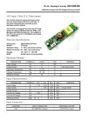
SPECIFICATION FOR APPROVAL - Adm Electronic
SPECIFICATION FOR APPROVAL - Adm Electronic
SPECIFICATION FOR APPROVAL - Adm Electronic

Create successful ePaper yourself
Turn your PDF publications into a flip-book with our unique Google optimized e-Paper software.
(<br />
)<br />
( V )<br />
Preliminary Specification<br />
Final Specification<br />
BUYER<br />
MODEL<br />
Title<br />
SIGNATURE<br />
/<br />
/<br />
/<br />
Product Specification<br />
<strong>SPECIFICATION</strong><br />
DATE<br />
Please return 1 copy for your confirmation with<br />
your signature and comments.<br />
<strong>FOR</strong><br />
<strong>APPROVAL</strong><br />
Ver. 1.1 Oct. 10, 2003<br />
10.4” VGA TFT LCD<br />
SUPPLIER<br />
*MODEL<br />
Suffix<br />
LB104V03<br />
Liquid Crystal Display<br />
LG.Philips LCD Co., Ltd.<br />
LB104V03<br />
A1<br />
*When you obtain standard approval,<br />
please use the above model name without suffix<br />
SIGNATURE<br />
S.H. Kang / G.Manager<br />
REVIEWED BY<br />
K. K. Jang / G. Manager<br />
S. C. Won / G. Manager<br />
PREPARED BY<br />
S. D. Cho/ Engineer<br />
S. H. Park / Engineer<br />
Products Engineering Dept.<br />
LG. Philips LCD Co., Ltd<br />
DATE<br />
1 / 24
No<br />
1<br />
2<br />
3<br />
4<br />
5<br />
6<br />
7<br />
8<br />
9<br />
3-1<br />
3-2<br />
3-3<br />
3-4<br />
3-5<br />
3-6<br />
7-1<br />
7-2<br />
8-1<br />
8-2<br />
A<br />
COVER<br />
CONTENTS<br />
RECORD OF REVISIONS<br />
GENERAL DESCRIPTION<br />
ABSOLUTE MAXIMUM RATINGS<br />
ELECTRICAL <strong>SPECIFICATION</strong>S<br />
ELECTRICAL CHARACTREISTICS<br />
INTERFACE CONNECTIONS<br />
SIGNAL TIMING <strong>SPECIFICATION</strong>S<br />
SIGNAL TIMING WAVE<strong>FOR</strong>MS<br />
COLOR INPUT DATA REFERNECE<br />
POWER SEQUENCE<br />
OPTICAL SFECIFICATIONS<br />
MECHANICAL CHARACTERISTICS<br />
RELIABLITY<br />
INTERNATIONAL STANDARDS<br />
SAFETY<br />
EMC<br />
PACKING<br />
DESIGNATION OF LOT MARK<br />
PACKING <strong>FOR</strong>M<br />
PRECAUTIONS<br />
Product Specification<br />
Contents<br />
ITEM<br />
APPENDIX. INCOMING INSPECTION STANDARD<br />
Ver. 1.1 Oct. 10, 2003<br />
LB104V03<br />
Liquid Crystal Display<br />
Page<br />
1<br />
2<br />
3<br />
4<br />
5<br />
6<br />
7<br />
9<br />
9<br />
10<br />
11<br />
12<br />
16<br />
20<br />
21<br />
21<br />
22<br />
22<br />
23<br />
25<br />
2 / 24
Revision No<br />
0.1<br />
0.2<br />
0.3<br />
1.0<br />
1.1<br />
Revision Date<br />
Mar. 14. 2003<br />
Jul. 22. 2003<br />
Aug. 19. 2003<br />
Sep. 01. 2003<br />
Oct. 10. 2003<br />
Page<br />
Product Specification<br />
RECORD OF REVISIONS<br />
Change Vibration test condition<br />
Ver. 1.1 Oct. 10, 2003<br />
-<br />
4<br />
13<br />
17<br />
18<br />
19<br />
20<br />
4<br />
6<br />
7<br />
7<br />
13<br />
17<br />
19<br />
-<br />
21<br />
First Draft (Preliminary)<br />
weight 480g � 500g(Max)<br />
Changing Color coordinates<br />
weight 480g � 500g<br />
Changing Mechanical drawing<br />
Changing Mechanical drawing<br />
Half sine wave, 100G �120G, 6ms �2ms<br />
weight 500g � 490g(Max)<br />
Insert Min value of Operating Voltage (455Vrms,7.0mArms)<br />
Insert Note 7 item (.. external inverter for 2 CCFLs.)<br />
Changing Connector marker<br />
Hirose or equivalent -> Hirose,LG Cable or equivalent<br />
insert Min value of Surface Luminance, white (320)<br />
weight 500 � 490g<br />
Changing Mechanical drawing<br />
Version 1.0(Final specification)<br />
Description<br />
LB104V03<br />
Liquid Crystal Display<br />
Note<br />
3 / 24
1. General Description<br />
General Features<br />
Active Screen Size<br />
Outline Dimension<br />
Pixel Pitch<br />
Pixel Format<br />
Color Depth<br />
Luminance, White<br />
Power Consumption<br />
Weight<br />
Display Operating Mode<br />
Surface Treatment<br />
Product Specification<br />
10.4 inches(26.42cm) diagonal<br />
236(H) × 180(V) × 10(D) mm<br />
0.33 mm × 0.33 mm<br />
640 horiz. By 480 vert. Pixels RGB strip arrangement<br />
6-bit, 262,144 colors<br />
400 cd/m 2 (Typ.) Lamp Ass’y replaceable<br />
6.3 Watt(Typ.)<br />
490g (Max.)<br />
Transmissive mode, normally white<br />
Ver. 1.1 Oct. 10, 2003<br />
Hard coating(3H) Anti-glare treatment of the front polarizer<br />
LB104V03<br />
Liquid Crystal Display<br />
The LB104V03-A1 is a Color Active Matrix Liquid Crystal Display with an integral Cold Cathode Fluorescent<br />
Lamp (CCFL) backlight system. The matrix employs a-Si Thin Film Transistor as the active element. It is a<br />
transmissive type display operating in the normally white mode. This TFT-LCD has 10.4 inches diagonally<br />
measured active display area with VGA resolution(480 vertical by 640 horizontal pixel array). Each pixel is<br />
divided into Red, Green and Blue sub-pixels or dots which are arranged in vertical stripes. Gray scale or the<br />
brightness of the sub-pixel color is determined with a 6-bit gray scale signal for each dot, thus, presenting a<br />
palette of more than 262,144 colors.<br />
The LB104V03-A1 is intended to support applications where thin thickness, low power are critical factors<br />
and graphic displays are important. In combination with the vertical arrangement of the sub-pixels, the<br />
LB104V03-A1 characteristics provide an excellent flat display for office automation products such as<br />
Notebook PC.<br />
POWER<br />
(VDD,GND)<br />
DISPLAY DATA &<br />
TIMING SIGNAL<br />
CN1<br />
GND<br />
INPUT CONNECTOR<br />
VBL CN2<br />
VBL<br />
GND<br />
CN3<br />
POWER SUPPLY<br />
TIMING<br />
CONTROLLER<br />
LAMP1<br />
G1<br />
G2<br />
GATE<br />
DRIVE<br />
CIRCUIT<br />
LAMP2<br />
G479<br />
G480<br />
SOURCE DRIVE CIRCUIT<br />
D1 D2 D1919D1920<br />
TFT-LCD<br />
(640 X 3 X 480)<br />
4 / 24
2. Absolute Maximum Ratings<br />
Product Specification<br />
Ver. 1.1 Oct. 10, 2003<br />
LB104V03<br />
Liquid Crystal Display<br />
The following are maximum values which, if exceeded, may cause faulty operation or damage to the unit.<br />
Power Input Voltage<br />
-20<br />
0<br />
Table 1. ABSOLUTE MAXIMUM RATINGS<br />
Values<br />
Parameter Symbol<br />
Units<br />
Notes<br />
Min Max<br />
Operating Temperature<br />
Storage Temperature<br />
Operating Ambient Humidity<br />
Storage Humidity<br />
Wet Bulb<br />
Temperature [ C]<br />
0<br />
10<br />
20<br />
30<br />
VCC<br />
TOP<br />
TST<br />
HOP<br />
HST<br />
40<br />
50<br />
10 20 30 40 50 60 70 80<br />
Dry Bulb Temperature [? ]<br />
0<br />
-20<br />
10<br />
10<br />
60<br />
90% 80%<br />
50<br />
60<br />
90<br />
90<br />
60%<br />
40%<br />
20%<br />
10%<br />
Humidity[(%)RH]<br />
°C<br />
°C<br />
%RH<br />
%RH<br />
Note : 1. Temperature and relative humidity range are shown in the figure below.<br />
Wet bulb temperature should be 39°C Max, and no condensation of water.<br />
-0.3<br />
4.0<br />
Vdc<br />
Storage<br />
Operation<br />
at 25 ± 5°C<br />
1<br />
1<br />
1<br />
1<br />
5 / 24
3. Electrical Specifications<br />
3-1. Electrical Characteristics<br />
Product Specification<br />
Ver. 1.1 Oct. 10, 2003<br />
LB104V03<br />
Liquid Crystal Display<br />
The LB104V03-A1 requires two power inputs. One is employed to power the LCD electronics and to drive<br />
the TFT array and liquid crystal. The second input which powers the CCFL, is typically generated by an<br />
inverter. The inverter is an external unit to the LCD.<br />
MODULE :<br />
Power Supply Input Voltage<br />
Power Supply Input Current<br />
Power Consumption<br />
LAMP :<br />
Operating Voltage<br />
Operating Current<br />
Established Starting Voltage<br />
Operating Frequency<br />
Discharge Stabilization Time<br />
Power Consumption<br />
Life Time<br />
Table 2. ELECTRICAL CHARACTERISTICS<br />
Parameter Symbol<br />
at 25 °C<br />
at 0 °C<br />
VCC<br />
I CC<br />
Pc<br />
V BL<br />
I BL<br />
Vs<br />
f BL<br />
Ts<br />
P BL<br />
Min<br />
3.0<br />
-<br />
-<br />
455<br />
(7.0mArms)<br />
2.0<br />
-<br />
-<br />
40<br />
-<br />
-<br />
40,000<br />
Values<br />
0.58<br />
485<br />
(6.0mArms)<br />
6.0<br />
-<br />
-<br />
55<br />
-<br />
5.8<br />
0.66<br />
625<br />
(2.0mArms)<br />
7.0<br />
750<br />
940<br />
80<br />
3<br />
6.4<br />
Watt<br />
V RMS<br />
mA RMS<br />
Note)<br />
The design of the inverter must have specifications for the lamp in LCD Assembly. The performance<br />
of the Lamp in LCM, for example life time or brightness, is extremely influenced by the characteristics of the<br />
DC-AC inverter. So all the parameters of an inverter should be carefully designed so as not to produce too<br />
much leakage current from high-voltage output of the inverter. When you design or order the inverter, please<br />
make sure unwanted lighting caused by the mismatch of the lamp and the inverter(no lighting, flicker, etc)<br />
never occurs. When you confirm it, the LCD Assembly should be operated in the same condition as installed<br />
in your instrument.<br />
1. VCC=3.3V, 25°C, f V (frame frequency) = 60Hz condition, whereas full black pattern is displayed.<br />
2. The variance of the voltage is ± 10%.<br />
3. The typical operating current is for the typical surface luminance (L WH ) in optical characteristics.<br />
4. The voltage above VS should be applied to the lamps for more than 1 second for start-up. Otherwise, the<br />
lamps may not be turned on. The used lamp current is the lamp typical current.<br />
Typ<br />
3.3<br />
175<br />
-<br />
Max<br />
3.6<br />
200<br />
-<br />
Unit<br />
Vdc<br />
mA<br />
V RMS<br />
V RMS<br />
kHz<br />
Min<br />
Watt<br />
Hrs<br />
Notes<br />
1<br />
1<br />
2<br />
3<br />
4<br />
5<br />
6<br />
7<br />
8<br />
6 / 24
Product Specification<br />
LB104V03<br />
Liquid Crystal Display<br />
5. The output of the inverter must have symmetrical(negative and positive) voltage waveform and<br />
symmetrical current waveform.(Unsymmetrical ratio is less than 10%) Please do not use the inverter<br />
which has unsymmetrical voltage and unsymmetrical current and spike wave.<br />
Lamp frequency may produce interference with horizontal synchronous frequency and as a result this<br />
may cause beat on the display. Therefore lamp frequency shall be as away possible from the horizontal<br />
synchronous frequency and from its harmonics in order to prevent interference.<br />
6. Let’s define the brightness of the lamp after being lighted for 5 minutes as 100%.<br />
T S is the time required for the brightness of the center of the lamp to be not less than 95%.<br />
7. The lamp power consumption shown above does not include loss of external inverter for 2 CCFLs.<br />
The used lamp current is the lamp typical current.<br />
8. The life time is determined as the time at which brightness of the lamp is 50% compared to that of initial<br />
value at the typical lamp current on condition of continuous operating at 25 ± 2°C.<br />
∗ Requirements for a system inverter design, which is intended to have a better display performance, a<br />
better power efficiency and a more reliable lamp, are following. It shall help increase the lamp lifetime and<br />
reduce leakage current.<br />
a. The asymmetry rate of the inverter waveform should be less than 10%.<br />
b. The distortion rate of the waveform should be within √2 ± 10%.<br />
* Inverter output waveform had better be more similar to ideal sine wave.<br />
I p<br />
I -p<br />
∗ Do not attach a conducting tape to lamp connecting wire.<br />
If the lamp wire attach to a conducting tape, TFT-LCD Module has a low luminance and the inverter<br />
has abnormal action. Because leakage current is occurred between lamp wire and conducting tape.<br />
3-2. Interface Connections<br />
Ver. 1.1 Oct. 10, 2003<br />
* Asymmetry rate:<br />
| I p – I –p | / I rms * 100%<br />
* Distortion rate<br />
I p (or I –p ) / I rms<br />
This LCD employs Three interface connections, a 30 pin connector is used for the module electronics interface<br />
and the other connectors are used for the integral backlight system.<br />
The electronics interface connector is a model KN10G-30S-1H manufactured by Hirose,<br />
GT101-30S-H16 manufactured by LG Cable or equivalent.<br />
(Mating connector: FI-X30M manufactured by JAE)<br />
Table 3. MODULE CONNECTOR PIN CONFIGURATION (CN1)<br />
7 / 24
Pin<br />
1<br />
2<br />
3<br />
4<br />
5<br />
6<br />
7<br />
8<br />
9<br />
10<br />
11<br />
12<br />
13<br />
14<br />
15<br />
16<br />
17<br />
18<br />
19<br />
20<br />
21<br />
22<br />
23<br />
24<br />
25<br />
26<br />
27<br />
28<br />
29<br />
30<br />
Symbol<br />
VCC<br />
VCC<br />
GND<br />
DCLK<br />
DTMG<br />
VSYNC<br />
HSYNC<br />
GND<br />
R0<br />
R1<br />
R2<br />
R3<br />
R4<br />
R5<br />
GND<br />
G0<br />
G1<br />
G2<br />
G3<br />
G4<br />
G5<br />
GND<br />
B0<br />
B1<br />
B2<br />
B3<br />
B4<br />
B5<br />
GND<br />
Description<br />
GND Ground<br />
Power (3.3V)<br />
Power (3.3V)<br />
Ground<br />
Data Clock<br />
Data Enable<br />
Vertical sync<br />
Horizontal sync<br />
Ground<br />
Red Data<br />
Red Data<br />
Red Data<br />
Red Data<br />
Red Data<br />
Red Data<br />
Ground<br />
Green Data<br />
Green Data<br />
Green Data<br />
Green Data<br />
Green Data<br />
Green Data<br />
Ground<br />
Blue Data<br />
Blue Data<br />
Blue Data<br />
Blue Data<br />
Blue Data<br />
Blue Data<br />
Ground<br />
Product Specification<br />
Ver. 1.1 Oct. 10, 2003<br />
LB104V03<br />
Liquid Crystal Display<br />
Notes<br />
[ I/F PIN ARRANGEMENT ]<br />
PWB<br />
Rear View<br />
Red data least significant bit (LSB)<br />
Red data most significant bit (MSB)<br />
Green data least significant bit (LSB)<br />
Green data most significant bit (MSB)<br />
Blue data least significant bit (LSB)<br />
Blue data most significant bit (MSB)<br />
The backlight interface connector is a model BHSR-02VS-1, manufactured by JST. The mating connector<br />
part number is SM02B-BHSS-1 or equivalent.<br />
Pin<br />
1<br />
Symbol Description<br />
Notes<br />
HV<br />
2 LV<br />
High Voltage (Pink color)<br />
Low Voltage (white color)<br />
30<br />
Pleas refer to page 19, for detail<br />
1<br />
-<br />
-<br />
8 / 24
3-3. Signal Timing Specifications<br />
DCLK<br />
Hsync<br />
Vsync<br />
DE<br />
DATA<br />
ITEM<br />
Frequency<br />
Width_Low<br />
Width_High<br />
Rise Time<br />
Fall Time<br />
Setup Time<br />
Hold Time<br />
Period<br />
Width_Active<br />
Rise/Fall Time<br />
Setup Time<br />
Hold Time<br />
Period<br />
Width_Active<br />
Rise/Fall Time<br />
Setup Time<br />
Hold Time<br />
Rise/Fall Time<br />
Horizontal<br />
Back Porch<br />
Horizontal<br />
Front Porch<br />
Vertical<br />
Back Porch<br />
Vertical<br />
Front Porch<br />
Hold Time<br />
Rise/Fall Time<br />
Symbol<br />
f CLK<br />
t WCL<br />
t WCH<br />
t rCLK<br />
t fCLK<br />
t SH<br />
t HH<br />
t HP<br />
t WH<br />
t Hr , t Hf<br />
Product Specification<br />
Table 5. TIMING TABLE<br />
515<br />
Ver. 1.1 Oct. 10, 2003<br />
t SV<br />
t HV<br />
t VP<br />
t WV<br />
t Vr , t Vf<br />
t SI<br />
t HI<br />
t Ir , t If<br />
t HBP<br />
t HFP<br />
t VBP<br />
t VFP<br />
Setup Time t SD<br />
t HD<br />
t Dr , t Df<br />
MIN.<br />
21<br />
8<br />
5<br />
-<br />
-<br />
3<br />
8<br />
770<br />
12<br />
-<br />
0<br />
2<br />
2<br />
-<br />
6<br />
1<br />
-<br />
12<br />
12<br />
5<br />
1<br />
6<br />
3<br />
-<br />
TYP.<br />
25.1<br />
-<br />
-<br />
-<br />
-<br />
-<br />
-<br />
800<br />
-<br />
-<br />
-<br />
-<br />
525<br />
-<br />
-<br />
-<br />
-<br />
-<br />
-<br />
-<br />
-<br />
-<br />
-<br />
-<br />
-<br />
MAX.<br />
28<br />
-<br />
-<br />
25<br />
25<br />
-<br />
-<br />
900<br />
120<br />
30<br />
-<br />
-<br />
560<br />
24<br />
50<br />
-<br />
-<br />
30<br />
-<br />
-<br />
-<br />
-<br />
-<br />
-<br />
25<br />
UNIT<br />
MHz<br />
ns<br />
ns<br />
t CLK<br />
ns<br />
ns<br />
t Hp<br />
ns<br />
ns<br />
ns<br />
t CLK<br />
t Hp<br />
ns<br />
ns<br />
LB104V03<br />
Liquid Crystal Display<br />
NOTE<br />
For Dclk<br />
For Hsync<br />
For Dclk<br />
For Dclk<br />
9 / 24
3-4. Signal Timing Waveforms<br />
DCLK, Hsync, Vsync, DE, DATA<br />
DCLK<br />
DATA<br />
DE<br />
DCLK<br />
Hsync<br />
Vsync<br />
Hsync<br />
DE<br />
Vsync<br />
DE<br />
t CLKL<br />
t WH<br />
t WV<br />
t CLK<br />
0.5V CC<br />
Invalid Data<br />
t HH<br />
t SV<br />
t HD<br />
Product Specification<br />
t SD<br />
Ver. 1.1 Oct. 10, 2003<br />
t HI<br />
t HBP<br />
t VBP<br />
t SH<br />
t SI<br />
t Hr ,t Vr<br />
t Ir ,t D ,t SD<br />
0.7V CC<br />
0.3V CC<br />
t WCH t WCL t fCLK t rCL<br />
K<br />
t HP<br />
t VP<br />
LB104V03<br />
Liquid Crystal Display<br />
t HFP<br />
tVFP<br />
t Hf ,t Vf<br />
t If ,t Df ,t HD<br />
Invalid Data<br />
t HV<br />
10 / 24
3-5. Color Input Data Reference<br />
Product Specification<br />
Ver. 1.1 Oct. 10, 2003<br />
LB104V03<br />
Liquid Crystal Display<br />
The brightness of each primary color (red,green and blue) is based on the 6-bit gray scale data input for the<br />
color ; the higher the binary input, the brighter the color. The table below provides a reference for color<br />
versus data input.<br />
Basic<br />
Color<br />
RED<br />
GREEN<br />
BLUE<br />
Color<br />
Red<br />
Green<br />
Blue<br />
Cyan<br />
Magenta<br />
Yellow<br />
White<br />
RED (00)<br />
RED (01)<br />
…<br />
RED (62)<br />
RED (63)<br />
GREEN (00)<br />
GREEN (01)<br />
...<br />
GREEN (62)<br />
GREEN (63)<br />
BLUE (00)<br />
BLUE (01)<br />
…<br />
BLUE (62)<br />
BLUE (63)<br />
Table 6. COLOR DATA REFERENCE<br />
RED<br />
MSB LSB<br />
R5 R4 R3 R2 R1 R0<br />
Black 0 0 0 0 0 0 0 0 0 0 0 0 0 0 0 0 0 0<br />
1 1 1 1 1 1<br />
0 0 0 0 0 0<br />
0 0 0 0 0 0<br />
0 0 0 0 0 0<br />
1 1 1 1 1 1<br />
1 1 1 1 1 1<br />
1 1 1 1 1 1<br />
0 0 0 0 0 0<br />
0 0 0 0 0 1<br />
…<br />
1 1 1 1 1 0<br />
1 1 1 1 1 1<br />
0 0 0 0 0 0<br />
0 0 0 0 0 0<br />
…<br />
0 0 0 0 0 0<br />
0 0 0 0 0 0<br />
0 0 0 0 0 0<br />
0 0 0 0 0 0<br />
…<br />
0 0 0 0 0 0<br />
0 0 0 0 0 0<br />
Input Color Data<br />
GREEN<br />
MSB LSB<br />
G5 G4 G3 G2 G1 G0<br />
0 0 0 0 0 0<br />
1 1 1 1 1 1<br />
0 0 0 0 0 0<br />
1 1 1 1 1 1<br />
0 0 0 0 0 0<br />
1 1 1 1 1 1<br />
1 1 1 1 1 1<br />
0 0 0 0 0 0<br />
0 0 0 0 0 0<br />
…<br />
0 0 0 0 0 0<br />
0 0 0 0 0 0<br />
0 0 0 0 0 0<br />
0 0 0 0 0 1<br />
…<br />
1 1 1 1 1 0<br />
1 1 1 1 1 1<br />
0 0 0 0 0 0<br />
0 0 0 0 0 0<br />
…<br />
0 0 0 0 0 0<br />
0 0 0 0 0 0<br />
BLUE<br />
MSB LSB<br />
B5 B4 B3 B2 B1 B0<br />
0 0 0 0 0 0<br />
0 0 0 0 0 0<br />
1 1 1 1 1 1<br />
1 1 1 1 1 1<br />
1 1 1 1 1 1<br />
0 0 0 0 0 0<br />
1 1 1 1 1 1<br />
0 0 0 0 0 0<br />
0 0 0 0 0 0<br />
…<br />
0 0 0 0 0 0<br />
0 0 0 0 0 0<br />
0 0 0 0 0 0<br />
0 0 0 0 0 0<br />
…<br />
0 0 0 0 0 0<br />
0 0 0 0 0 0<br />
0 0 0 0 0 0<br />
0 0 0 0 0 1<br />
…<br />
1 1 1 1 1 0<br />
1 1 1 1 1 1<br />
11 / 24
3-6. Power Sequence<br />
Power supply for LCD ( VCC)<br />
Interface Signal (Tx)<br />
Power for Lamp<br />
Parameter<br />
T 1<br />
T 2<br />
T 3<br />
T 4<br />
T 5<br />
T 6<br />
T 7<br />
Min.<br />
400<br />
Product Specification<br />
Ver. 1.1 Oct. 10, 2003<br />
-<br />
0<br />
200<br />
200<br />
0<br />
-<br />
10% 10%<br />
0V<br />
0V<br />
90% 90%<br />
LB104V03<br />
Liquid Crystal Display<br />
Note)<br />
1. Please avoid floating state of interface signal at invalid period.<br />
2. When the interface signal is invalid, be sure to pull down the power supply for LCD VCC to 0V.<br />
3. Lamp power must be turn on after power supply for LCD and interface signal are valid.<br />
T1<br />
Value<br />
Typ.<br />
-<br />
-<br />
-<br />
-<br />
-<br />
-<br />
-<br />
T2<br />
Valid data<br />
10% 10%<br />
T3 T4<br />
Table 7. POWER SEQUENCE TABLE<br />
Max.<br />
10<br />
50<br />
-<br />
-<br />
50<br />
10<br />
-<br />
T5<br />
T6<br />
OFF ON<br />
OFF<br />
Units<br />
(ms)<br />
(ms)<br />
(ms)<br />
(ms)<br />
(ms)<br />
(ms)<br />
(ms)<br />
T7<br />
12 / 24
4. Optical Specification<br />
Response Time<br />
Color Coordinates<br />
Viewing Angle<br />
Product Specification<br />
FIG. 1 Optical Characteristic Measurement Equipment and Method<br />
WHITE<br />
x axis, left (Φ=180°)<br />
y axis, up (Φ=90°)<br />
y axis, down (Φ=270°)<br />
Table 8. OPTICAL CHARACTERISTICS<br />
Ver. 1.1 Oct. 10, 2003<br />
BY<br />
WX<br />
LB104V03<br />
Liquid Crystal Display<br />
Optical characteristics are determined after the unit has been ‘ON’ and stable for approximately 30 minutes in<br />
a dark environment at 25°C. The values specified are at an approximate distance 50cm from the LCD surface<br />
at a viewing angle of Φ and Θ equal to 0°.<br />
FIG. 1 presents additional information concerning the measurement equipment and method.<br />
Optical Stage(x,y)<br />
Contrast Ratio<br />
Luminance Variation<br />
Ta=25°C, VCC=3.3V, fV=60Hz, Dclk= 25.1MHz, V IN=3.3V, I L=6.0mA<br />
Values<br />
Parameter Symbol Units Notes<br />
Min Typ MAx<br />
Surface Luminance, white<br />
Rise Time<br />
Decay Time<br />
RED<br />
GREEN<br />
BLUE<br />
LCD Module<br />
CR<br />
L WH<br />
δ WHITE<br />
Tr R<br />
Tr D<br />
RX<br />
RY<br />
GX<br />
GY<br />
BX<br />
WY<br />
0.087<br />
0.275<br />
0.107<br />
0.295<br />
0.127<br />
0.315<br />
x axis, right(Φ=0°) Θr 50 60 - degree<br />
Θl<br />
Θu<br />
Θd<br />
50cm<br />
-<br />
320<br />
-<br />
-<br />
-<br />
0.614<br />
0.331<br />
0.275<br />
0.547<br />
0.126<br />
0.305<br />
50<br />
35<br />
45<br />
300<br />
400<br />
1.25<br />
5<br />
20<br />
0.634<br />
0.351<br />
0.295<br />
0.567<br />
0.146<br />
0.325<br />
60<br />
40<br />
50<br />
-<br />
-<br />
1.45<br />
8<br />
25<br />
0.654<br />
0.371<br />
0.315<br />
0.587<br />
0.166<br />
0.345<br />
-<br />
-<br />
-<br />
Pritchard 880 or<br />
equivalent<br />
cd/m 2<br />
ms<br />
ms<br />
degree<br />
degree<br />
degree<br />
1<br />
2<br />
3<br />
4<br />
5<br />
13 / 24
Product Specification<br />
Note)<br />
1. Contrast Ratio(CR) is defined mathematically as<br />
Surface Luminance with all white pixels<br />
Contrast Ratio =<br />
Surface Luminance with all black pixels<br />
Ver. 1.1 Oct. 10, 2003<br />
LB104V03<br />
Liquid Crystal Display<br />
2. Surface luminance is the center point across the LCD surface 50cm from the surface with all pixels<br />
displaying white. For more information see FIG 1.<br />
3. The variation in surface luminance , The Panel total variation (δ WHITE) is determined by measuring L N<br />
at each test position 1 through 5, and then dividing the maximum L N of 5 points luminance by<br />
minimum L N of 5 points luminance. For more information see FIG 2.<br />
δ WHITE = Maximum(L 1 ,L 2 , … L 5 ) / Minimum(L 1 ,L 2 , … L 5 )<br />
4. Response time is the time required for the display to transition from white to black (rise time, Tr R ) and<br />
from black to white(Decay Time, Tr D ). For additional information see FIG 3.<br />
5. Viewing angle is the angle at which the contrast ratio is greater than 10. The angles are determined<br />
for the horizontal or x axis and the vertical or y axis with respect to the z axis which is normal to the<br />
LCD surface. For more information see FIG 4.<br />
6. Gray scale specification * f V =60Hz<br />
Gray Level<br />
L0<br />
L7<br />
L15<br />
L23<br />
L31<br />
L39<br />
L47<br />
L55<br />
L63<br />
Luminance [%] (Typ)<br />
0.2<br />
0.8<br />
4.5<br />
11.0<br />
22.0<br />
35.5<br />
52.5<br />
74.0<br />
100<br />
14 / 24
FIG. 2 Luminance<br />
Product Specification<br />
<br />
V<br />
FIG. 3 Response Time<br />
Ver. 1.1 Oct. 10, 2003<br />
LB104V03<br />
Liquid Crystal Display<br />
The response time is defined as the following figure and shall be measured by switching the input signal<br />
for “black” and “white”.<br />
Optical<br />
V/2<br />
Response<br />
V/4<br />
100<br />
90<br />
10<br />
0<br />
%<br />
H/4<br />
white<br />
H/2<br />
Tr R<br />
H<br />
L2 L3<br />
L1<br />
Center Point<br />
L4 L5<br />
black<br />
Tr D<br />
H,V : ACTIVE AREA<br />
white<br />
15 / 24
FIG. 4 Viewing angle<br />
φ = 180°<br />
,<br />
Left<br />
φ = 270°<br />
,<br />
Down<br />
Product Specification<br />
<br />
Normal<br />
Ver. 1.1 Oct. 10, 2003<br />
θ<br />
φ<br />
Eye<br />
Y<br />
φ = 90°, Up<br />
φ = 0°<br />
,<br />
Right<br />
LB104V03<br />
Liquid Crystal Display<br />
16 / 24
5. Mechanical Characteristics<br />
Product Specification<br />
Ver. 1.1 Oct. 10, 2003<br />
LB104V03<br />
Liquid Crystal Display<br />
The contents provide general mechanical characteristics for the model LB104V03-A1. In addition the figures<br />
in the next page are detailed mechanical drawing of the LCD.<br />
Outline Dimension<br />
Bezel Area<br />
Active Display Area<br />
Weight<br />
Surface Treatment<br />
Horizontal<br />
Vertical<br />
Depth<br />
Horizontal<br />
Vertical<br />
Horizontal<br />
Vertical<br />
490(Max.)<br />
163 ± 0.5mm<br />
158.4 mm<br />
Hard coating(3H)<br />
Anti-glare treatment of the front polarizer<br />
236.0 ± 0.5mm<br />
180.0 ± 0.5mm<br />
Max. 10.5mm<br />
215.6 ± 0.5mm<br />
211.2mm<br />
17 / 24
Product Specification<br />
LB104V03<br />
Liquid Crystal Display<br />
Note) Unit:[mm], General tolerance: ± 0.5mm<br />
Ver. 1.1 Oct. 10, 2003<br />
18 / 24
Product Specification<br />
LB104V03<br />
Liquid Crystal Display<br />
Note) Unit:[mm], General tolerance: ± 0.5mm<br />
Ver. 1.1 Oct. 10, 2003<br />
19 / 24
7. International Standards<br />
7-1. Safety<br />
Product Specification<br />
Ver. 1.1 Oct. 10, 2003<br />
LB104V03<br />
Liquid Crystal Display<br />
a) UL 60950, Third Edition, Underwriters Laboratories, Inc., Dated Dec. 11, 2000.<br />
Standard for Safety of Information Technology Equipment, Including Electrical Business Equipment.<br />
b) CAN/CSA C22.2, No. 60950, Third Edition, Canadian Standards Association, Dec. 1, 2000.<br />
Standard for Safety of Information Technology Equipment, Including Electrical Business Equipment.<br />
c) EN 60950 : 2000, Third Edition<br />
IEC 60950 : 1999, Third Edition<br />
European Committee for Electrotechnical Standardization(CENELEC)<br />
EUROPEAN STANDARD for Safety of Information Technology Equipment Including Electrical Business<br />
Equipment.<br />
7-2. EMC<br />
a) ANSI C63.4 “Methods of Measurement of Radio-Noise Emissions from Low-Voltage Electrical and<br />
Electrical Equipment in the Range of 9kHZ to 40GHz. “American National Standards Institute(ANSI),<br />
1992<br />
b) C.I.S.P.R “Limits and Methods of Measurement of Radio Interface Characteristics of Information<br />
Technology Equipment.“ International Special Committee on Radio Interference.<br />
c) EN 55022 “Limits and Methods of Measurement of Radio Interface Characteristics of Information<br />
Technology Equipment.“ European Committee for Electrotechnical Standardization.(CENELEC), 1998<br />
( Including A1: 2000 )<br />
20 / 24
6. Reliability<br />
Environment test condition<br />
No.<br />
1<br />
2<br />
3<br />
4<br />
5<br />
6<br />
7<br />
Test Item<br />
High temperature storage test<br />
Low temperature storage test<br />
High temperature operation test<br />
Low temperature operation test<br />
Vibration test (non-operating)<br />
Shock test (non-operating)<br />
Altitude operating<br />
storage / shipment<br />
Product Specification<br />
Ver. 1.1 Oct. 10, 2003<br />
Ta= 60°C, 240h<br />
Ta= -20°C, 240h<br />
Ta= 50°C, 50%RH, 240h<br />
Ta= 0°C, 240h<br />
Conditions<br />
Random 1.0Grms 3axis(X,Y,Z ), 1hrs/axis<br />
Bandwidth : 10~500Hz<br />
Half sine wave, 120G, 2ms<br />
one shock of each six faces<br />
0 ~ 10,000 feet (3,048m) 24Hr<br />
0 ~ 40,000 feet (12,192m) 24Hr<br />
LB104V03<br />
Liquid Crystal Display<br />
{ Result Evaluation Criteria }<br />
There should be no change which might affect the practical display function when the display quality<br />
test is conducted under normal operating condition.<br />
21 / 24
8. Packing<br />
8-1. Designation of Lot Mark<br />
a) Lot Mark<br />
Product Specification<br />
A B C D E F G H I J K L M<br />
A,B,C : Inch<br />
D : Year<br />
E : Month<br />
F : Panel Code<br />
G : Factory Code<br />
H : Assembly Code<br />
I,J,K,L,M : Serial No<br />
Note<br />
1. Year<br />
Year<br />
Mark<br />
2. Month<br />
Month<br />
Mark<br />
3. Panel Code<br />
Panel Code<br />
Mark<br />
4. Factory Code<br />
Factory Code<br />
Mark<br />
5. Serial No<br />
Serial No.<br />
Mark<br />
Serial NO. is printed on the label. The label is attached to the backside of the LCD module.<br />
This is subject to change without prior notice.<br />
8-2. Packing Form<br />
97<br />
7<br />
Jan<br />
1<br />
a) Package quantity in one box : 10 pcs<br />
2000<br />
b) Box Size :L323mm X W270mm X H262mm<br />
Ver. 1.1 Oct. 10, 2003<br />
98<br />
8<br />
Feb<br />
2<br />
P1 Factory<br />
1<br />
LPL Gumi<br />
K<br />
99<br />
9<br />
Mar<br />
4<br />
1 ~ 99,999<br />
00001 ~ 99999<br />
0<br />
Apr<br />
4<br />
P2 Factory<br />
2<br />
LPL Nanjing<br />
C<br />
2001<br />
1<br />
May<br />
5<br />
2002<br />
2<br />
Jun<br />
6<br />
P3 Factory<br />
3<br />
100,000 ~<br />
2003<br />
3<br />
Jul<br />
7<br />
2004<br />
4<br />
Aug<br />
A0001 ~ A9999, - - - - , Z9999<br />
8<br />
P4 Factory<br />
4<br />
2005<br />
5<br />
Sep<br />
9<br />
LB104V03<br />
Liquid Crystal Display<br />
P5 Factory<br />
5<br />
2006<br />
6<br />
Oct<br />
A<br />
2007<br />
7<br />
Nov<br />
B<br />
H<br />
Dec<br />
C<br />
Hydis Panel<br />
22 / 24
9. PRECAUTIONS<br />
Product Specification<br />
Please pay attention to the followings when you use this TFT LCD module.<br />
9-1. MOUNTING PRECAUTIONS<br />
Ver. 1.1 Oct. 10, 2003<br />
LB104V03<br />
Liquid Crystal Display<br />
(1) You must mount a module using holes arranged in four corners or four sides.<br />
(2) You should consider the mounting structure so that uneven force (ex. Twisted stress) is not applied to the<br />
module. And the case on which a module is mounted should have sufficient strength so that external<br />
force is not transmitted directly to the module.<br />
(3) Please attach the surface transparent protective plate to the surface in order to protect the polarizer.<br />
Transparent protective plate should have sufficient strength in order to the resist external force.<br />
(4) You should adopt radiation structure to satisfy the temperature specification.<br />
(5) Acetic acid type and chlorine type materials for the cover case are not desirable because the former<br />
generates corrosive gas of attacking the polarizer at high temperature and the latter causes circuit break<br />
by electro-chemical reaction.<br />
(6) Do not touch, push or rub the exposed polarizers with glass, tweezers or anything harder than HB<br />
pencil lead. And please do not rub with dust clothes with chemical treatment.<br />
Do not touch the surface of polarizer for bare hand or greasy cloth.(Some cosmetics are detrimental<br />
to the polarizer.)<br />
(7) When the surface becomes dusty, please wipe gently with absorbent cotton or other soft materials like<br />
chamois soaks with petroleum benzene. Normal-hexane is recommended for cleaning the adhesives<br />
used to attach front / rear polarizers. Do not use acetone, toluene and alcohol because they cause<br />
chemical damage to the polarizer.<br />
(8) Wipe off saliva or water drops as soon as possible. Their long time contact with polarizer causes<br />
deformations and color fading.<br />
(9) Do not open the case because inside circuits do not have sufficient strength.<br />
9-2. OPERATING PRECAUTIONS<br />
(1) The spike noise causes the mis-operation of circuits. It should be lower than following voltage :<br />
V=± 200mV(Over and under shoot voltage)<br />
(2) Response time depends on the temperature.(In lower temperature, it becomes longer.)<br />
(3) Brightness depends on the temperature. (In lower temperature, it becomes lower.)<br />
And in lower temperature, response time(required time that brightness is stable after turned on) becomes<br />
longer.<br />
(4) Be careful for condensation at sudden temperature change. Condensation makes damage to polarizer or<br />
electrical contacted parts. And after fading condensation, smear or spot will occur.<br />
(5) When fixed patterns are displayed for a long time, remnant image is likely to occur.<br />
(6) Module has high frequency circuits. Sufficient suppression to the electromagnetic interference shall be<br />
done by system manufacturers. Grounding and shielding methods may be important to minimized the<br />
interference.<br />
23 / 24
Product Specification<br />
9-3. ELECTROSTATIC DISCHARGE CONTROL<br />
Ver. 1.1 Oct. 10, 2003<br />
LB104V03<br />
Liquid Crystal Display<br />
Since a module is composed of electronic circuits, it is not strong to electrostatic discharge. Make certain that<br />
treatment persons are connected to ground through wrist band etc. And don’t touch interface pin directly.<br />
9-4. PRECAUTIONS <strong>FOR</strong> STRONG LIGHT EXPOSURE<br />
Strong light exposure causes degradation of polarizer and color filter.<br />
9-5. STORAGE<br />
When storing modules as spares for a long time, the following precautions are necessary.<br />
(1) Store them in a dark place. Do not expose the module to sunlight or fluorescent light. Keep the<br />
temperature between 5°C and 35°C at normal humidity.<br />
(2) The polarizer surface should not come in contact with any other object.<br />
It is recommended that they be stored in the container in which they were shipped.<br />
9-6. HANDLING PRECAUTIONS <strong>FOR</strong> PROTECTION FILM<br />
(1) The protection film is attached to the bezel with a small masking tape.<br />
When the protection film is peeled off, static electricity is generated between the film and polarizer.<br />
This should be peeled off slowly and carefully by people who are electrically grounded and with well<br />
ion-blown equipment or in such a condition, etc.<br />
(2) When the module with protection film attached is stored for a long time, sometimes there remains a<br />
very small amount of glue still on the bezel after the protection film is peeled off.<br />
(3) You can remove the glue easily. When the glue remains on the bezel surface or its vestige is<br />
recognized, please wipe them off with absorbent cotton waste or other soft material like chamois<br />
soaked with normal-hexane.<br />
24 / 24