Download FT245R datasheet - DigChip
Download FT245R datasheet - DigChip
Download FT245R datasheet - DigChip

You also want an ePaper? Increase the reach of your titles
YUMPU automatically turns print PDFs into web optimized ePapers that Google loves.
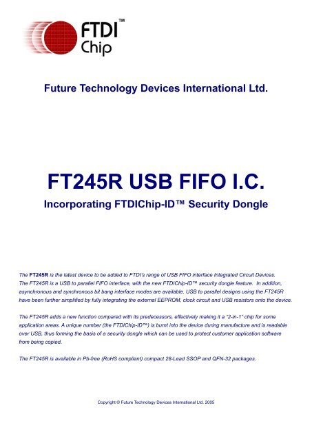
Future Technology Devices International Ltd.<br />
<strong>FT245R</strong> USB FIFO I.C.<br />
Incorporating FTDIChip-ID Security Dongle<br />
The <strong>FT245R</strong> is the latest device to be added to FTDI’s range of USB FIFO interface Integrated Circuit Devices.<br />
The <strong>FT245R</strong> is a USB to parallel FIFO interface, with the new FTDIChip-ID security dongle feature. In addition,<br />
asynchronous and synchronous bit bang interface modes are available. USB to parallel designs using the <strong>FT245R</strong><br />
have been further simplified by fully integrating the external EEPROM, clock circuit and USB resistors onto the device.<br />
The <strong>FT245R</strong> adds a new function compared with its predecessors, effectively making it a “2-in-1” chip for some<br />
application areas. A unique number (the FTDIChip-ID) is burnt into the device during manufacture and is readable<br />
over USB, thus forming the basis of a security dongle which can be used to protect customer application software<br />
from being copied.<br />
The <strong>FT245R</strong> is available in Pb-free (RoHS compliant) compact 28-Lead SSOP and QFN-32 packages.<br />
Copyright © Future Technology Devices International Ltd. 2005
1. Features<br />
Page 2<br />
1.1 Hardware Features<br />
• Single chip USB to parallel FIFO bidirectional data<br />
transfer interface.<br />
• Entire USB protocol handled on the chip - No<br />
USB-specific firmware programming required.<br />
• Simple interface to MCU / PLD / FPGA logic with<br />
simple 4-wire handshake interface.<br />
• Data transfer rate to 1 Megabyte / second - D2XX<br />
Direct Drivers.<br />
• Data transfer rate to 300 kilobyte / second - VCP<br />
Drivers.<br />
• FTDI’s royalty-free VCP and D2XX drivers<br />
eliminate the requirement for USB driver<br />
development in most cases.<br />
• New USB FTDIChip-ID feature.<br />
• FIFO receive and transmit buffers for high data<br />
throughput.<br />
• Adjustable receive buffer timeout.<br />
• Synchronous and asynchronous bit bang mode<br />
interface options with RD# and WR# strobes allow<br />
the data bus to be used as a general purpose I/O<br />
port.<br />
• Integrated 1024 Bit internal EEPROM for storing<br />
USB VID, PID, serial number and product<br />
description strings.<br />
• Device supplied preprogrammed with unique USB<br />
serial number.<br />
• Support for USB suspend / resume through<br />
PWREN# pin and Wake Up pin function.<br />
• In-built support for event characters.<br />
• Support for bus powered, self powered, and highpower<br />
bus powered USB configurations.<br />
• Integrated 3.3V level converter for USB I/O .<br />
• Integrated level converter on FIFO interface and<br />
control pins for interfacing to 5V - 1.8V Logic.<br />
• True 5V / 3.3V / 2.8V / 1.8V CMOS drive output<br />
and TTL input.<br />
• High I/O pin output drive option.<br />
• Integrated USB resistors.<br />
• Integrated power-on-reset circuit.<br />
• Fully integrated clock - no external crystal,<br />
oscillator, or resonator required.<br />
• Fully integrated AVCC supply filtering - No separate<br />
AVCC pin and no external R-C filter required.<br />
• USB bulk transfer mode.<br />
• 3.3V to 5.25V Single Supply Operation.<br />
• Low operating and USB suspend current.<br />
• Low USB bandwidth consumption.<br />
• UHCI / OHCI / EHCI host controller compatible<br />
• USB 2.0 Full Speed compatible.<br />
• -40°C to 85°C extended operating temperature<br />
range.<br />
• Available in compact Pb-free 28 Pin SSOP and<br />
QFN-32 packages (both RoHS compliant).<br />
1.2 Driver Support<br />
Royalty-Free VIRTUAL COM PORT<br />
(VCP) DRIVERS for...<br />
• Windows 98, 98SE, ME, 2000, Server 2003, XP.<br />
• Windows Vista / Longhorn*<br />
• Windows XP 64-bit.*<br />
• Windows XP Embedded.<br />
• Windows CE.NET 4.2 & 5.0<br />
• MAC OS 8 / 9, OS-X<br />
• Linux 2.4 and greater<br />
Royalty-Free D2XX Direct Drivers<br />
(USB Drivers + DLL S/W Interface)<br />
• Windows 98, 98SE, ME, 2000, Server 2003, XP.<br />
• Windows Vista / Longhorn*<br />
• Windows XP 64-bit.*<br />
• Windows XP Embedded.<br />
• Windows CE.NET 4.2 & 5.0<br />
• Linux 2.4 and greater<br />
The drivers listed above are all available to download for free from the FTDI website. Various 3rd Party Drivers are<br />
also available for various other operating systems - see the FTDI website for details.<br />
* Currently Under Development. Contact FTDI for availability.<br />
1.3 Typical Applications<br />
• Upgrading Legacy Peripherals to USB<br />
• Cellular and Cordless Phone USB data transfer<br />
cables and interfaces<br />
• Interfacing MCU / PLD / FPGA based designs to<br />
USB<br />
• USB Audio and Low Bandwidth Video data transfer<br />
• PDA to USB data transfer<br />
• USB Smart Card Readers<br />
• USB Instrumentation<br />
• USB Industrial Control<br />
• USB MP3 Player Interface<br />
• USB FLASH Card Reader / Writers<br />
• Set Top Box PC - USB interface<br />
• USB Digital Camera Interface<br />
• USB Hardware Modems<br />
• USB Wireless Modems<br />
• USB Bar Code Readers<br />
• USB Software / Hardware Encryption Dongles<br />
<strong>FT245R</strong> USB UART I.C. Datasheet Version 1.02 © Future Technology Devices International Ltd. 2005
2. Enhancements<br />
Page 3<br />
2.1 Device Enhancements and Key Features<br />
This section summarises the enhancements and the key features of the <strong>FT245R</strong> device. For further details, consult<br />
the device pin-out description and functional description sections.<br />
Integrated Clock Circuit - Previous generations of FTDI’s USB to parallel FIFO interface devices required an external<br />
crystal or ceramic resonator. The clock circuit has now been integrated onto the device meaning that no crystal or<br />
ceramic resonator is required. However, if required, an external 12MHz crystal can be used as the clock source.<br />
Integrated EEPROM - Previous generations of FTDI’s USB to parallel FIFO interface devices required an external<br />
EEPROM if the device were to use USB Vendor ID (VID), Product ID (PID), serial number and product description<br />
strings other than the default values in the device itself. This external EEPROM has now been integrated onto the<br />
<strong>FT245R</strong> chip meaning that all designs have the option to change the product description strings. A user area of the<br />
internal EEPROM is available for storing additional data. The internal EEPROM is programmable in circuit, over USB<br />
without any additional voltage requirement.<br />
Preprogrammed EEPROM - The <strong>FT245R</strong> is supplied with its internal EEPROM preprogrammed with a serial number<br />
which is unique to each individual device. This, in most cases, will remove the need to program the device EEPROM.<br />
Integrated USB Resistors - Previous generations of FTDI’s USB to parallel FIFO interface devices required two<br />
external series resistors on the USBDP and USBDM lines, and a 1.5 kΩ pull up resistor on USBDP. These three<br />
resistors have now been integrated onto the device.<br />
Integrated AVCC Filtering - Previous generations of FTDI’s USB to parallel FIFO interface devices had a separate<br />
AVCC pin - the supply to the internal PLL. This pin required an external R-C filter. The separate AVCC pin is now<br />
connected internally to VCC, and the filter has now been integrated onto the chip.<br />
Less External Components - Integration of the crystal, EEPROM, USB resistors, and AVCC filter will substantially<br />
reduce the bill of materials cost for USB interface designs using the <strong>FT245R</strong> compared to its FT245BM predecessor.<br />
Enhanced Asynchronous Bit Bang Mode with RD# and WR# Strobes - The <strong>FT245R</strong> supports FTDI’s BM chip bit<br />
bang mode. In bit bang mode, the eight parallel FIFO data bus lines can be switched from the regular interface mode<br />
to an 8-bit general purpose I/O port. Data packets can be sent to the device and they will be sequentially sent to the<br />
interface at a rate controlled by an internal timer (equivalent to the baud rate prescaler). With the <strong>FT245R</strong> device this<br />
mode has been enhanced so that the internal RD# and WR# strobes are now brought out of the device which can be<br />
used to allow external logic to be clocked by accesses to the bit bang I/O bus. This option will be described more fully<br />
in a separate application note<br />
Synchronous Bit Bang Mode - Synchronous bit bang mode differs from asynchronous bit bang mode in that the<br />
interface pins are only read when the device is written to. Thus making it easier for the controlling program to measure<br />
the response to an output stimulus as the data returned is synchronous to the output data. The feature was previously<br />
seen in FTDI’s FT2232C device. This option will be described more fully in a separate application note.<br />
Lower Supply Voltage - Previous generations of the chip required 5V supply on the VCC pin. The <strong>FT245R</strong> will work<br />
with a Vcc supply in the range 3.3V - 5V. Bus powered designs would still take their supply from the 5V on the USB<br />
bus, but for self powered designs where only 3.3V is available, and there is no 5V supply, there is no longer any need<br />
for an additional external regulator.<br />
Integrated Level Converter on FIFO Interface and Control Signals - VCCIO pin supply can be from 1.8V to 5V.<br />
Connecting the VCCIO pin to 1.8V, 2.8V, or 3.3V allows the device to directly interface to 1.8V, 2.8V or 3.3V and other<br />
logic families without the need for external level converter I.C.s<br />
5V / 3.3V / 2.8V / 1.8V Logic Interface - The <strong>FT245R</strong> provides true CMOS Drive Outputs and TTL level Inputs.<br />
Integrated Power-On-Reset (POR) Circuit- The device incorporates an internal POR function. A RESET# pin is<br />
available in order to allow external logic to reset the <strong>FT245R</strong> where required. However, for many applications the<br />
RESET# pin can be left unconnected, or pulled up to VCCIO.<br />
<strong>FT245R</strong> USB UART I.C. Datasheet Version 1.02 © Future Technology Devices International Ltd. 2005
Page 4<br />
Wake Up Function - If USB is in suspend mode, and remote wake up has been enabled in the internal EEPROM (it is<br />
enabled by default), the RXF# pin becomes an input. Strobing this pin low will cause the <strong>FT245R</strong> to request a resume<br />
from suspend on the USB bus. Normally this can be used to wake up the host PC from suspend<br />
Lower Operating and Suspend Current - The device operating supply current has been further reduced to 15mA,<br />
and the suspend current has been reduced to around 70μA. This allows a greater margin for peripherals to meet the<br />
USB suspend current limit of 500μA.<br />
Low USB Bandwidth Consumption - The operation of the USB interface to the <strong>FT245R</strong> has been designed to use<br />
as little as possible of the total USB bandwidth available from the USB host controller.<br />
High Output Drive Option - The parallel FIFO interface and the four FIFO handshake pins can be made to drive<br />
out at three times the standard signal drive level thus allowing multiple devices to be driven, or devices that require a<br />
greater signal drive strength to be interfaced to the <strong>FT245R</strong>. This option is configured in the internal EEPROM.<br />
Power Management Control for USB Bus Powered, High Current Designs- The PWREN# signal can be used to<br />
directly drive a transistor or P-Channel MOSFET in applications where power switching of external circuitry is required.<br />
An option in the internal EEPROM makes the device gently pull down on its FIFO interface lines when the power<br />
is shut off (PWREN# is high). In this mode any residual voltage on external circuitry is bled to GND when power is<br />
removed, thus ensuring that external circuitry controlled by PWREN# resets reliably when power is restored.<br />
FTDIChip-ID - Each <strong>FT245R</strong> is assigned a unique number which is burnt into the device at manufacture. This ID<br />
number cannot be reprogrammed by product manufacturers or end-users. This allows the possibility of using <strong>FT245R</strong><br />
based dongles for software licensing. Further to this, a renewable license scheme can be implemented based on the<br />
FTDIChip-ID number when encrypted with other information. This encrypted number can be stored in the user area<br />
of the <strong>FT245R</strong> internal EEPROM, and can be decrypted, then compared with the protected FTDIChip-ID to verify<br />
that a license is valid. Web based applications can be used to maintain product licensing this way. An application note<br />
describing this feature is available separately from the FTDI website.<br />
Improved EMI Performance - The reduced operating current and improved on-chip VCC decoupling significantly<br />
improves the ease of PCB design requirements in order to meet FCC, CE and other EMI related specifications.<br />
Programmable FIFO TX Buffer Timeout - The FIFO TX buffer timeout is used to flush remaining data from the<br />
receive buffer. This timeout defaults to 16ms, but is programmable over USB in 1ms increments from 1ms to 255ms,<br />
thus allowing the device to be optimised for protocols that require fast response times from short data packets.<br />
Extended Operating Temperature Range - The FT232R operates over an extended temperature range of -40º to<br />
+85º C thus allowing the device to be used in automotive and industrial applications.<br />
New Package Options - The <strong>FT245R</strong> is available in two packages - a compact 28 pin SSOP ( <strong>FT245R</strong>L) and an<br />
ultra-compact 5mm x 5mm pinless QFN-32 package ( <strong>FT245R</strong>Q). Both packages are lead ( Pb ) free, and use a<br />
‘green’ compound. Both packages are fully compliant with European Union directive 2002/95/EC.<br />
<strong>FT245R</strong> USB UART I.C. Datasheet Version 1.02 © Future Technology Devices International Ltd. 2005
3. Block Diagram<br />
Page 5<br />
3.1 Block Diagram (Simplified)<br />
VCC<br />
PWREN#<br />
3V3OUT<br />
USBDP<br />
USBDM<br />
3.3 Volt<br />
LDO<br />
Regulator<br />
USB<br />
Transceiver<br />
with<br />
Integrated<br />
Series<br />
Resistors<br />
and 1.5K<br />
Pull-up<br />
Serial Interface<br />
Engine<br />
( SIE )<br />
To USB<br />
Transceiver<br />
Cell<br />
FIFO TX Buffer<br />
USB<br />
Protocol Engine<br />
Internal<br />
EEPROM<br />
VCCIO<br />
FIFO Controller<br />
with<br />
Programmable<br />
High Drive<br />
D0<br />
D1<br />
D2<br />
D3<br />
D4<br />
D5<br />
D6<br />
D7<br />
RD#<br />
WR<br />
RXF#<br />
TXE#<br />
USB DPLL<br />
3V3OUT<br />
OSCO<br />
(optional)<br />
OCSI<br />
(optional)<br />
Internal<br />
12MHz<br />
Oscillator<br />
Clock<br />
Multiplier<br />
48MHz<br />
FIFO RX Buffer<br />
RESET#<br />
To USB Transceiver Cell<br />
RESET<br />
GENERATOR<br />
TEST<br />
GND<br />
Figure 1 - <strong>FT245R</strong> Block Diagram<br />
3.2 Functional Block Descriptions<br />
3.3V LDO Regulator - The 3.3V LDO Regulator generates the 3.3V reference voltage for driving the USB transceiver<br />
cell output buffers. It requires an external decoupling capacitor to be attached to the 3V3OUT regulator output pin. It<br />
also provides 3.3V power to the 1.5kΩ internal pull up resistor on USBDP. The main function of this block is to power<br />
the USB Transceiver and the Reset Generator Cells, rather than to power external logic. However, external circuitry<br />
requiring 3.3V nominal at a current of around 50mA could also draw its power from the 3V3OUT pin if required.<br />
USB Transceiver - The USB Transceiver Cell provides the USB 1.1 / USB 2.0 full-speed physical interface to the USB<br />
cable. The output drivers provide 3.3V level slew rate control signalling, whilst a differential receiver and two single<br />
ended receivers provide USB data in, SEO and USB Reset condition detection. This Cell also incorporates internal<br />
USB series resistors on the USB data lines, and a 1.5kΩ pull up resistor on USBDP.<br />
USB DPLL - The USB DPLL cell locks on to the incoming NRZI USB data and provides separate recovered clock and<br />
data signals to the SIE block.<br />
Internal 12MHz Oscillator - The Internal 12MHz Oscillator cell generates a 12MHz reference clock input to the x4<br />
Clock multiplier. The 12MHz Oscillator is also used as the reference clock for the SIE, USB Protocol Engine and FIFO<br />
controller blocks<br />
Clock Multiplier - The Clock Multiplier takes the 12MHz input from the Oscillator Cell and generates the 48MHz clock<br />
reference used for the USB DPLL block.<br />
Serial Interface Engine (SIE) - The Serial Interface Engine (SIE) block performs the Parallel to Serial and Serial to<br />
Parallel conversion of the USB data. In accordance to the USB 2.0 specification, it performs bit stuffing / un-stuffing<br />
and CRC5 / CRC16 generation / checking on the USB data stream.<br />
<strong>FT245R</strong> USB UART I.C. Datasheet Version 1.02 © Future Technology Devices International Ltd. 2005
Page 6<br />
USB Protocol Engine - The USB Protocol Engine manages the data stream from the device USB control endpoint. It<br />
handles the low level USB protocol (Chapter 9) requests generated by the USB host controller and the commands for<br />
controlling the functional parameters of the FIFO.<br />
FIFO TX Buffer - Data written into the FIFO using the WR pin is stored in the FIFO TX (transmit) Buffer. The USB host<br />
controller removes data from the FIFO TX Buffer by sending a USB request for data from the device data In endpoint.<br />
FIFO RX Buffer - Data sent from the USB host controller to the FIFO via the USB data Out endpoint is stored in the<br />
FIFO RX (receive) buffer and is removed from the buffer by reading the contents of the FIFO using the RD# pin.<br />
FIFO Controller - The FIFO controller handles the transfer of data between the external FIFO interface pins (D0 - D7)<br />
and the FIFO transmit and receive buffers. A new feature, which is enabled in the internal EEPROM allows high signal<br />
drive strength on the FIFO parallel data bus and handshake control pins.<br />
RESET Generator - The integrated Reset Generator Cell provides a reliable power-on reset to the device internal<br />
circuitry on power up. A RESET# input is provided to allow other devices to reset the <strong>FT245R</strong>. RESET# can be tied<br />
to VCCIO or left unconnected, unless there is a requirement to reset the <strong>FT245R</strong> device from external logic or an<br />
external reset generator I.C.<br />
Internal EEPROM - The internal EEPROM in the <strong>FT245R</strong> can be used to store USB Vendor ID (VID), Product ID<br />
(PID), device serial number, product description string, and various other USB configuration descriptors. The device is<br />
supplied with the internal EEPROM settings preprogrammed as described in Section 10.<br />
<strong>FT245R</strong> USB UART I.C. Datasheet Version 1.02 © Future Technology Devices International Ltd. 2005
4. Device Pin Out and Signal Descriptions<br />
4.1 28-LD SSOP Package<br />
Page 7<br />
D0<br />
1<br />
28<br />
OSCO<br />
D4<br />
OSCI<br />
D2<br />
TEST<br />
VCCIO<br />
D1<br />
D7<br />
GND<br />
NC<br />
D5<br />
D6<br />
D3<br />
PWREN#<br />
RD#<br />
YYXX-A<br />
<strong>FT245R</strong>L<br />
FTDI<br />
AGND<br />
NC<br />
RXF#<br />
TXE#<br />
GND<br />
VCC<br />
RESET#<br />
GND<br />
3V3OUT<br />
USBDM<br />
WR<br />
14 15<br />
USBDP<br />
Figure 2 - 28 Pin SSOP Package Pin Out<br />
4<br />
20<br />
16<br />
15<br />
VCCIO<br />
VCC<br />
USBDM<br />
USBDP<br />
D0<br />
D1<br />
D2<br />
D3<br />
1<br />
5<br />
3<br />
11<br />
8<br />
19<br />
24<br />
27<br />
28<br />
NC<br />
RESET#<br />
NC<br />
OSCI<br />
OSCO<br />
<strong>FT245R</strong>L<br />
D4<br />
D5<br />
D6<br />
D7<br />
2<br />
9<br />
10<br />
6<br />
RXF#<br />
23<br />
17<br />
3V3OUT<br />
A<br />
G<br />
N<br />
D<br />
G<br />
N<br />
D<br />
G<br />
N<br />
D<br />
G<br />
N<br />
D<br />
25 7 18 21 26<br />
T<br />
E<br />
S<br />
T<br />
TXE#<br />
RD#<br />
WR<br />
PWREN#<br />
22<br />
13<br />
14<br />
12<br />
Figure 3 - 28 Pin SSOP Package Pin Out (Schematic Symbol)<br />
<strong>FT245R</strong> USB UART I.C. Datasheet Version 1.02 © Future Technology Devices International Ltd. 2005
4.2 SSOP-28 Package Signal Descriptions<br />
Page 8<br />
Table 1 - SSOP Package Pin Out Description<br />
Pin No. Name Type Description<br />
USB Interface Group<br />
15 USBDP I/O USB Data Signal Plus, incorporating internal series resistor and 1.5kΩ pull up resistor to 3.3V<br />
16 USBDM I/O USB Data Signal Minus, incorporating internal series resistor.<br />
Power and Ground Group<br />
4 VCCIO PWR +1.8V to +5.25V supply to the FIFO Interface and Control group pins (1...3, 5, 6, 9...14, 22, 23). In USB bus<br />
powered designs connect to 3V3OUT to drive out at 3.3V levels, or connect to VCC to drive out at 5V CMOS<br />
level. This pin can also be supplied with an external 1.8V - 2.8V supply in order to drive out at lower levels. It<br />
should be noted that in this case this supply should originate from the same source as the supply to Vcc. This<br />
means that in bus powered designs a regulator which is supplied by the 5V on the USB bus should be used.<br />
7, 18, 21 GND PWR Device ground supply pins<br />
17 3V3OUT Output 3.3V output from integrated L.D.O. regulator. This pin should be decoupled to ground using a 100nF capacitor.<br />
The prime purpose of this pin is to provide the internal 3.3V supply to the USB transceiver cell and the internal<br />
1.5kΩ pull up resistor on USBDP. Up to 50mA can be drawn from this pin to power external logic if required.<br />
This pin can also be used to supply the <strong>FT245R</strong>’s VCCIO pin.<br />
20 VCC PWR 3.3V to 5.25V supply to the device core.<br />
25 AGND PWR Device analog ground supply for internal clock multiplier<br />
Miscellaneous Signal Group<br />
8, 24 NC NC No internal connection.<br />
19 RESET# Input Can be used by an external device to reset the <strong>FT245R</strong>. If not required can be left unconnected or pulled up<br />
to VCCIO.<br />
26 TEST Input Puts the device into I.C. test mode. Must be grounded for normal operation.<br />
27 OSCI Input Input to 12MHz Oscillator Cell. Optional - Can be left unconnected for normal operation. *<br />
28 OSCO Output Output from 12MHz Oscillator Cell. Optional - Can be left unconnected for normal operation if internal oscillator<br />
is used.*<br />
FIFO Interface and Control Group<br />
1 D0 I/O FIFO Data Bus Bit 0**<br />
2 D4 I/O FIFO Data Bus Bit 4**<br />
3 D2 I/O FIFO Data Bus Bit 2**<br />
5 D1 I/O FIFO Data Bus Bit 1**<br />
6 D7 I/O FIFO Data Bus Bit 7**<br />
9 D5 I/O FIFO Data Bus Bit 5**<br />
10 D6 I/O FIFO Data Bus Bit 6**<br />
11 D3 I/O FIFO Data Bus Bit 3**<br />
12 PWREN# Output Goes low after the device is configured by USB, then high during USB suspend. Can be used to control power<br />
to external logic P-Channel logic level MOSFET switch. Enable the interface pull-down option when using the<br />
PWREN# pin in this way.<br />
13 RD# Input Enables the current FIFO data byte on D0...D7 when low. Fetched the next FIFO data byte (if available) from<br />
the receive FIFO buffer when RD# goes from high to low. See Section 4.5 for timing diagram. **<br />
14 WR Input Writes the data byte on the D0...D7 pins into the transmit FIFO buffer when WR goes from high to low. See<br />
Section 4.5 for timing diagram. **<br />
22 TXE# Output When high, do not write data into the FIFO. When low, data can be written into the FIFO by strobing WR high,<br />
then low. During reset this signal pin is tri-state, but pulled up to VCCIO via an internal 200kΩ resistor. See<br />
Section 4.5 for timing diagram.<br />
23 RXF# Output When high, do not read data from the FIFO. When low, there is data available in the FIFO which can be read<br />
by strobing RD# low, then high again. During reset this signal pin is tri-state, but pulled up to VCCIO via an<br />
internal 200kΩ resistor. See Section 4.5 for timing diagram.<br />
If the Remote Wakeup option is enabled in the internal EEPROM, during USB suspend mode (PWREN# = 1)<br />
RXF# becomes an input which can be used to wake up the USB host from suspend mode. Strobing the pin<br />
low will cause the device to request a resume on the USB bus.<br />
*Contact FTDI Support for details of how to use an external crystal, ceramic resonator, or oscillator with the <strong>FT245R</strong>.<br />
** When used in Input Mode, these pins are pulled to VCCIO via internal 200kΩ resistors. These can be programmed<br />
to gently pull low during USB suspend ( PWREN# = “1” ) by setting this option in the internal EEPROM.<br />
<strong>FT245R</strong> USB UART I.C. Datasheet Version 1.02 © Future Technology Devices International Ltd. 2005
4.3 QFN-32 Package<br />
TOP<br />
32 25<br />
Page 9<br />
1<br />
8<br />
FTDI<br />
YYXX-A<br />
<strong>FT245R</strong>Q<br />
24<br />
17<br />
9<br />
16<br />
BOTTOM<br />
NC<br />
OSCO<br />
OSCI<br />
TEST<br />
NC<br />
D2<br />
D4<br />
D0<br />
25 26 27 28 29 30 31 32<br />
AGND 24<br />
NC 23<br />
RXF# 22<br />
TXE# 21<br />
GND 20<br />
VCC 19<br />
RESET# 18<br />
GND 17<br />
1 VCCIO<br />
2 D1<br />
3 D7<br />
4 GND<br />
5 NC<br />
6 D5<br />
7 D6<br />
8 D3<br />
16<br />
15<br />
14<br />
13<br />
12<br />
11<br />
10<br />
9<br />
Figure 4 - QFN-32 Package Pin Out<br />
3V3OUT<br />
USBDM<br />
USBDP<br />
NC<br />
NC<br />
WR<br />
RD#<br />
PWREN#<br />
1<br />
19<br />
15<br />
14<br />
5<br />
12<br />
13<br />
25<br />
29<br />
VCCIO<br />
VCC<br />
USBDM<br />
USBDP<br />
NC<br />
NC<br />
NC<br />
NC<br />
NC<br />
<strong>FT245R</strong>Q<br />
D0<br />
D1<br />
D2<br />
D3<br />
D4<br />
D5<br />
D6<br />
30<br />
2<br />
32<br />
8<br />
31<br />
6<br />
7<br />
18<br />
23<br />
27<br />
28<br />
16<br />
RESET#<br />
NC<br />
OSCI<br />
OSCO<br />
3V3OUT<br />
A<br />
G<br />
N<br />
D<br />
G<br />
N<br />
D<br />
G<br />
N<br />
D<br />
G<br />
N<br />
D<br />
24 4 17 20 26<br />
T<br />
E<br />
S<br />
T<br />
D6<br />
RXF#<br />
TXE#<br />
RD#<br />
WR<br />
PWREN#<br />
3<br />
22<br />
21<br />
10<br />
11<br />
9<br />
Figure 5 - QFN-32 Package Pin Out (Schematic Symbol)<br />
<strong>FT245R</strong> USB UART I.C. Datasheet Version 1.02 © Future Technology Devices International Ltd. 2005
4.4 QFN-32 Package Signal Descriptions<br />
Page 10<br />
Table 2 - QFN Package Pin Out Description<br />
Pin No. Name Type Description<br />
USB Interface Group<br />
14 USBDP I/O USB Data Signal Plus, incorporating internal series resistor and 1.5kΩ pull up resistor to 3.3V<br />
15 USBDM I/O USB Data Signal Minus, incorporating internal series resistor.<br />
Power and Ground Group<br />
1 VCCIO PWR +1.8V to +5.25V supply to FIFO Interface and Control group pins (2,3, 6, ...,11, 21, 22, 30,..32). In USB bus<br />
powered designs connect to 3V3OUT to drive out at 3.3V levels, or connect to VCC to drive out at 5V CMOS<br />
level. This pin can also be supplied with an external 1.8V - 2.8V supply in order to drive out at lower levels. It<br />
should be noted that in this case this supply should originate from the same source as the supply to Vcc. This<br />
means that in bus powered designs a regulator which is supplied by the 5V on the USB bus should be used.<br />
4, 17, 20 GND PWR Device ground supply pins<br />
16 3V3OUT Output 3.3V output from integrated L.D.O. regulator. This pin should be decoupled to ground using a 100nF capacitor.<br />
The prime purpose of this pin is to provide the internal 3.3V supply to the USB transceiver cell and the internal<br />
1.5kΩ pull up resistor on USBDP. Up to 50mA can be drawn from this pin to power external logic if required.<br />
This pin can also be used to supply the <strong>FT245R</strong>’s VCCIO pin.<br />
19 VCC PWR 3.3V to 5.25V supply to the device core.<br />
24 AGND PWR Device analog ground supply for internal clock multiplier<br />
Miscellaneous Signal Group<br />
5, 12, 13,<br />
23, 25, 29<br />
NC NC No internal connection.<br />
18 RESET# Input Can be used by an external device to reset the <strong>FT245R</strong>. If not required can be left unconnected or pulled up<br />
to VCCIO.<br />
26 TEST Input Puts the device into I.C. test mode. Must be grounded for normal operation.<br />
27 OSCI Input Input to 12MHz Oscillator Cell. Optional - Can be left unconnected for normal operation. *<br />
28 OSCO Output Output from 12MHz Oscillator Cell. Optional - Can be left unconnected for normal operation if internal oscillator<br />
is used. *<br />
FIFO Interface and Control Group<br />
30 D0 I/O FIFO Data Bus Bit 0**<br />
31 D4 I/O FIFO Data Bus Bit 4**<br />
32 D2 I/O FIFO Data Bus Bit 2**<br />
2 D1 I/O FIFO Data Bus Bit 1**<br />
3 D7 I/O FIFO Data Bus Bit 7**<br />
6 D5 I/O FIFO Data Bus Bit 5**<br />
7 D6 I/O FIFO Data Bus Bit 6**<br />
8 D3 I/O FIFO Data Bus Bit 3**<br />
9 PWREN# Output Goes low after the device is configured by USB, then high during USB suspend. Can be used to control power<br />
to external logic P-Channel logic level MOSFET switch. Enable the interface pull-down option when using the<br />
PWREN# pin in this way.<br />
10 RD# Input Enables the current FIFO data byte on D0...D7 when low. Fetched the next FIFO data byte (if available) from<br />
the receive FIFO buffer when RD# goes from high to low. See Section 4.5 for timing diagram. **<br />
11 WR Input Writes the data byte on the D0...D7 pins into the transmit FIFO buffer when WR goes from high to low. See<br />
Section 4.5 for timing diagram. **<br />
21 TXE# Output When high, do not write data into the FIFO. When low, data can be written into the FIFO by strobing WR high,<br />
then low. During reset this signal pin is tri-state, but pulled up to VCCIO via an internal 200kΩ resistor. See<br />
Section 4.5 for timing diagram.<br />
22 RXF# Output When high, do not read data from the FIFO. When low, there is data available in the FIFO which can be read<br />
by strobing RD# low, then high again. During reset this signal pin is tri-state, but pulled up to VCCIO via an<br />
internal 200kΩ resistor. See Section 4.5 for timing diagram.<br />
If the Remote Wakeup option is enabled in the internal EEPROM, during USB suspend mode (PWREN# = 1)<br />
RXF# becomes an input which can be used to wake up the host from suspend mode. Strobing the pin low will<br />
cause the device to request a resume on the USB bus.<br />
*Contact FTDI Support for details of how to use an external crystal, ceramic resonator, or oscillator with the <strong>FT245R</strong>.<br />
** When used in Input Mode, these pins are pulled to VCCIO via internal 200kΩ resistors. These can be programmed<br />
to gently pull low during USB suspend ( PWREN# = “1” ) by setting this option in the internal EEPROM.<br />
<strong>FT245R</strong> USB UART I.C. Datasheet Version 1.02 © Future Technology Devices International Ltd. 2005
Page 11<br />
4.5 <strong>FT245R</strong> FIFO Timing Diagrams<br />
Figure 6 - FIFO Read Cycle<br />
RXF#<br />
T5<br />
T6<br />
RD#<br />
T1<br />
T2<br />
D[7...0]<br />
T3<br />
Valid Data<br />
T4<br />
Table 3 - FIFO Read Cycle Timings<br />
Time Description Min Max Unit<br />
T1 RD Active Pulse Width 50 ns<br />
T2 RD to RD Pre-Charge Time 50 + T6 ns<br />
T3 RD Active to Valid Data* 20 50 ns<br />
T4 Valid Data Hold Time from RD Inactive* 0 ns<br />
T5 RD Inactive to RXF# 0 25 ns<br />
T6 RXF Inactive After RD Cycle 80 ns<br />
* Load = 30pF<br />
Figure 7 - FIFO Write Cycle<br />
T11<br />
T12<br />
TXE#<br />
T7<br />
T8<br />
WR<br />
T9<br />
T10<br />
D[7...0]<br />
Valid Data<br />
Table 4 - FIFO Write Cycle Timings<br />
Time Description Min Max Unit<br />
T7 WR Active Pulse Width 50 ns<br />
T8 WR to RD Pre-Charge Time 50 ns<br />
T9 Data Setup Time before WR Inactive 20 ns<br />
T10 Data Hold Time from WR Inactive 0 ns<br />
T11 WR Inactive to TXE# 5 25 ns<br />
T12 TXE Inactive After WR Cycle 80 ns<br />
<strong>FT245R</strong> USB UART I.C. Datasheet Version 1.02 © Future Technology Devices International Ltd. 2005
5. Package Parameters<br />
Page 12<br />
The <strong>FT245R</strong> is supplied in two different packages. The <strong>FT245R</strong>L is the SSOP-28 option and the <strong>FT245R</strong>Q is the<br />
QFN-32 package option. The solder reflow profile for both packages is described in Section 5.3.<br />
5.1 SSOP-28 Package Dimensions<br />
7.80 +/-0.40<br />
5.30 +/-0.30<br />
0.30 +/-0.012<br />
1<br />
1.02 Typ.<br />
28<br />
0.05 Min<br />
1.75<br />
+/- 0.10<br />
2.00 Max<br />
0.65 +/-0.026<br />
YYXX-A<br />
<strong>FT245R</strong>L<br />
FTDI<br />
10.20 +/-0.30<br />
0.09<br />
0.75 +/-0.20<br />
12° Typ<br />
1.25 +/-0.12<br />
0° - 8°<br />
0.25<br />
14 15<br />
Figure 8 - SSOP-28 Package Dimensions<br />
The <strong>FT245R</strong>L is supplied in a RoHS compliant 28 pin SSOP package. The package is lead ( Pb ) free and uses a<br />
‘green’ compound. The package is fully compliant with European Union directive 2002/95/EC.<br />
This package has a 5.30mm x 10.20mm body ( 7.80mm x 10.20mm including pins ). The pins are on a 0.65 mm pitch.<br />
The above mechanical drawing shows the SSOP-28 package – all dimensions are in millimetres.<br />
The date code format is YYXX where XX = 2 digit week number, YY = 2 digit year number.<br />
<strong>FT245R</strong> USB UART I.C. Datasheet Version 1.02 © Future Technology Devices International Ltd. 2005
Page 13<br />
5.2 QFN-32 Package Dimensions<br />
TOP<br />
32 25<br />
Indicates Pin #1<br />
(Laser Marked)<br />
1<br />
8<br />
FTDI<br />
YYXX-A<br />
<strong>FT245R</strong>Q<br />
24<br />
17<br />
5.000<br />
9<br />
16<br />
5.000<br />
BOTTOM<br />
0.500<br />
24<br />
23<br />
25 26 27 28 29 30 31 32<br />
1<br />
2<br />
0.150 Max<br />
Pin #1 ID<br />
0.250<br />
+/-0.050<br />
22<br />
21<br />
20<br />
19<br />
18<br />
3<br />
4<br />
5<br />
6<br />
7<br />
3.200 +/-0.100<br />
17<br />
8<br />
0.200 Min<br />
16<br />
15<br />
14<br />
13<br />
12<br />
11<br />
10<br />
9<br />
0.500<br />
+/-0.050<br />
3.200 +/-0.100<br />
SIDE<br />
0.800<br />
+/-0.050<br />
0.200<br />
0.050<br />
Figure 9 - QFN-32 Package Dimensions<br />
0.900<br />
+/-0.100<br />
The <strong>FT245R</strong>Q is supplied in a RoHS compliant leadless QFN-32 package. The package is lead ( Pb ) free, and uses<br />
a ‘green’ compound. The package is fully compliant with European Union directive 2002/95/EC.<br />
This package has a compact 5.00mm x 5.00mm body. The solder pads are on a 0.50mm pitch. The above mechanical<br />
drawing shows the QFN-32 package – all dimensions are in millimetres.<br />
The centre pad on the base of the <strong>FT245R</strong>Q is not internally connected, and can be left unconnected, or connected to<br />
ground (recommended).<br />
The date code format is YYXX where XX = 2 digit week number, YY = 2 digit year number.<br />
<strong>FT245R</strong> USB UART I.C. Datasheet Version 1.02 © Future Technology Devices International Ltd. 2005
Page 14<br />
5.3 Solder Reflow Profile<br />
The <strong>FT245R</strong> is supplied in Pb free 28 LD SSOP and QFN-32 packages. The recommended solder reflow profile for<br />
both package options is shown in Figure 10.<br />
t p<br />
Temperature, T (Degrees C)<br />
T p<br />
T L<br />
T Max S<br />
T Min S<br />
tS<br />
Preheat<br />
Ramp Up<br />
t L<br />
Critical Zone: when<br />
T is in the range<br />
T to Tp<br />
Ramp<br />
Down<br />
L<br />
25<br />
Figure 10 - <strong>FT245R</strong> Solder Reflow Profile<br />
T = 25º C to T P<br />
Time, t (seconds)<br />
The recommended values for the solder reflow profile are detailed in Table 5. Values are shown for both a completely<br />
Pb free solder process (i.e. the <strong>FT245R</strong> is used with Pb free solder), and for a non-Pb free solder process (i.e. the<br />
<strong>FT245R</strong> is used with non-Pb free solder).<br />
Table 5 - Reflow Profile Parameter Values<br />
Profile Feature Pb Free Solder Process Non-Pb Free Solder Process<br />
Average Ramp Up Rate (T s<br />
to T p<br />
) 3°C / second Max. 3°C / Second Max.<br />
Preheat<br />
- Temperature Min (T S<br />
Min.)<br />
- Temperature Max (T S<br />
Max.)<br />
- Time (t S<br />
Min to t S<br />
Max)<br />
Time Maintained Above Critical Temperature T L<br />
:<br />
- Temperature (T L<br />
)<br />
- Time (t L<br />
)<br />
150°C<br />
200°C<br />
60 to 120 seconds<br />
217°C<br />
60 to 150 seconds<br />
100°C<br />
150°C<br />
60 to 120 seconds<br />
183°C<br />
60 to 150 seconds<br />
Peak Temperature (T P<br />
) 260°C 240°C<br />
Time within 5°C of actual Peak Temperature (t P<br />
) 20 to 40 seconds 20 to 40 seconds<br />
Ramp Down Rate 6°C / second Max. 6°C / second Max.<br />
Time for T= 25°C to Peak Temperature, T p<br />
8 minutes Max. 6 minutes Max.<br />
<strong>FT245R</strong> USB UART I.C. Datasheet Version 1.02 © Future Technology Devices International Ltd. 2005
6. Device Characteristics and Ratings<br />
Page 15<br />
6.1 Absolute Maximum Ratings<br />
The absolute maximum ratings for the <strong>FT245R</strong> devices are as follows. These are in accordance with the Absolute<br />
Maximum Rating System (IEC 60134). Exceeding these may cause permanent damage to the device.<br />
Table 6 - Absolute Maximum Ratings<br />
Parameter Value Unit<br />
Storage Temperature -65°C to 150°C Degrees C<br />
Floor Life (Out of Bag) At Factory Ambient<br />
( 30°C / 60% Relative Humidity)<br />
168 Hours<br />
(IPC/JEDEC J-STD-033A MSL<br />
Level 3 Compliant)*<br />
Ambient Temperature (Power Applied) -40°C to 85°C Degrees C.<br />
Vcc Supply Voltage -0.5 to +6.00 V<br />
D.C. Input Voltage - USBDP and USBDM -0.5 to +3.8 V<br />
D.C. Input Voltage - High Impedance Bidirectionals -0.5 to +(Vcc +0.5) V<br />
D.C. Input Voltage - All other Inputs -0.5 to +(Vcc +0.5) V<br />
D.C. Output Current - Outputs 24 mA<br />
DC Output Current - Low Impedance Bidirectionals 24 mA<br />
Power Dissipation (Vcc = 5.25V) 500 mW<br />
* If devices are stored out of the packaging beyond this time limit the devices should be baked before use. The<br />
devices should be ramped up to a temperature of 125°C and baked for up to 17 hours.<br />
6.2 DC Characteristics<br />
DC Characteristics ( Ambient Temperature = -40 o C to +85 o C )<br />
Table 7 - Operating Voltage and Current<br />
Parameter Description Min Typ Max Units Conditions<br />
Vcc1 VCC Operating Supply Voltage 3.3 - 5.25 V<br />
Vcc2 VCCIO Operating Supply Voltage 1.8 - 5.25 V<br />
Icc1 Operating Supply Current - 15 - mA Normal Operation<br />
Icc2 Operating Supply Current 50 70 100 μA USB Suspend<br />
Hours<br />
Table 8 - FIFO Interface and Control Bus Pin Characteristics (VCCIO = 5.0V, Standard Drive Level)<br />
Parameter Description Min Typ Max Units Conditions<br />
Voh Output Voltage High 3.2 4.1 4.9 V I source = 2mA<br />
Vol Output Voltage Low 0.3 0.4 0.6 V I sink = 2mA<br />
Vin Input Switching Threshold 1.3 1.6 1.9 V **<br />
VHys Input Switching Hysteresis 50 55 60 mV **<br />
Table 9 - FIFO Interface and Control Bus Pin Characteristics (VCCIO = 3.3V, Standard Drive Level)<br />
Parameter Description Min Typ Max Units Conditions<br />
Voh Output Voltage High 2.2 2.7 3.2 V I source = 1mA<br />
Vol Output Voltage Low 0.3 0.4 0.5 V I sink = 2mA<br />
Vin Input Switching Threshold 1.0 1.2 1.5 V **<br />
VHys Input Switching Hysteresis 20 25 30 mV **<br />
<strong>FT245R</strong> USB UART I.C. Datasheet Version 1.02 © Future Technology Devices International Ltd. 2005
Table 10 - FIFO Interface and Control Bus Pin Characteristics (VCCIO = 2.8V, Standard Drive Level)<br />
Parameter Description Min Typ Max Units Conditions<br />
Voh Output Voltage High 2.1 2.6 3.1 V I source = 1mA<br />
Page 16<br />
Vol Output Voltage Low 0.3 0.4 0.5 V I sink = 2 mA<br />
Vin Input Switching Threshold 1.0 1.2 1.5 V **<br />
VHys Input Switching Hysteresis 20 25 30 mV **<br />
Table 11 - FIFO Interface and Control Bus Pin Characteristics (VCCIO = 5.0V, High Drive Level)<br />
Parameter Description Min Typ Max Units Conditions<br />
Voh Output Voltage High 3.2 4.1 4.9 V I source = 6mA<br />
Vol Output Voltage Low 0.3 0.4 0.6 V I sink = 6mA<br />
Vin Input Switching Threshold 1.3 1.6 1.9 V **<br />
VHys Input Switching Hysteresis 50 55 60 mV **<br />
Table 12 - FIFO Interface and Control Bus Pin Characteristics (VCCIO = 3.3V, High Drive Level)<br />
Parameter Description Min Typ Max Units Conditions<br />
Voh Output Voltage High 2.2 2.8 3.2 V I source = 3mA<br />
Vol Output Voltage Low 0.3 0.4 0.6 V I sink = 8mA<br />
Vin Input Switching Threshold 1.0 1.2 1.5 V **<br />
VHys Input Switching Hysteresis 20 25 30 mV **<br />
Table 13 - FIFO Interface and Control Bus Pin Characteristics (VCCIO = 2.8V, High Drive Level)<br />
Parameter Description Min Typ Max Units Conditions<br />
Voh Output Voltage High 2.1 2.8 3.2 V I source = 3mA<br />
Vol Output Voltage Low 0.3 0.4 0.6 V I sink = 8mA<br />
Vin Input Switching Threshold 1.0 1.2 1.5 V **<br />
VHys Input Switching Hysteresis 20 25 30 mV **<br />
**Inputs have an internal 200kΩ pull-up resistor to VCCIO.<br />
Table 14 - RESET#, TEST Pin Characteristics<br />
Parameter Description Min Typ Max Units Conditions<br />
Vin Input Switching Threshold 1.3 1.6 1.9 V<br />
VHys Input Switching Hysteresis 50 55 60 mV<br />
Table 15 - USB I/O Pin (USBDP, USBDM) Characteristics<br />
Parameter Description Min Typ Max Units Conditions<br />
UVoh I/O Pins Static Output ( High) 2.8 3.6 V RI = 1.5kΩ to 3V3OUT ( D+ )<br />
RI = 15kΩ to GND ( D- )<br />
UVol I/O Pins Static Output ( Low ) 0 0.3 V RI = 1.5kΩ to 3V3OUT ( D+ )<br />
RI = 15kΩ to GND ( D- )<br />
UVse Single Ended Rx Threshold 0.8 2.0 V<br />
UCom Differential Common Mode 0.8 2.5 V<br />
UVDif Differential Input Sensitivity 0.2 V<br />
UDrvZ Driver Output Impedance 26 29 44 Ohms ***<br />
***Driver Output Impedance includes the internal USB series resistors on USBDP and USBDM pins.<br />
<strong>FT245R</strong> USB UART I.C. Datasheet Version 1.02 © Future Technology Devices International Ltd. 2005
6.3 EEPROM Reliability Characteristics<br />
Page 17<br />
The internal 1024 Bit EEPROM has the following reliability characteristics-<br />
Table 16 - EEPROM Characteristics<br />
Parameter Description Value Unit<br />
Data Retention 15 Years<br />
Read / Write Cycles 100,000 Cycles<br />
6.4 Internal Clock Characteristics<br />
The internal Clock Oscillator has the following characteristics.<br />
Table 17 - Internal Clock Characteristics<br />
Parameter Value Unit<br />
Min Typical Max<br />
Frequency of Operation 11.98 12.00 12.02 MHz<br />
Clock Period 83.19 83.33 83.47 ns<br />
Duty Cycle 45 50 55 %<br />
Table 18 - OSCI, OSCO Pin Characteristics (Optional - Only applies if external Oscillator is used***)<br />
Parameter Description Min Typ Max Units Conditions<br />
Voh Output Voltage High 2.8 - 3.6 V Fosc = 12MHz<br />
Vol Output Voltage Low 0.1 - 1.0 V Fosc = 12MHz<br />
Vin Input Switching Threshold 1.8 2.5 3.2 V<br />
***When supplied the device is configured to use its internal clock oscillator. Users who wish to use an external<br />
oscillator or crystal should contact FTDI technical support.<br />
<strong>FT245R</strong> USB UART I.C. Datasheet Version 1.02 © Future Technology Devices International Ltd. 2005
7. Device Configurations<br />
Page 18<br />
Please note that pin numbers on the <strong>FT245R</strong> chip in this section have deliberately been left out as they vary between<br />
the <strong>FT245R</strong>L and <strong>FT245R</strong>Q versions of the device. All of these configurations apply to both package options for the<br />
<strong>FT245R</strong> device. Please refer to Section 4 for the package option pin-out and signal descriptions.<br />
7.1 Bus Powered Configuration<br />
5<br />
SHIELD<br />
1<br />
2<br />
3<br />
4<br />
10nF<br />
+<br />
GND<br />
Ferrite<br />
Bead<br />
Vcc<br />
VCC<br />
USBDM<br />
USBDP<br />
VCCIO<br />
NC<br />
RESET#<br />
NC<br />
OSCI<br />
OSCO<br />
<strong>FT245R</strong><br />
D0<br />
D1<br />
D2<br />
D3<br />
D4<br />
D5<br />
D6<br />
D7<br />
Vcc<br />
RXF#<br />
TXE#<br />
100nF<br />
4.7uF<br />
+<br />
100nF<br />
3V3OUT<br />
A<br />
G<br />
N<br />
D<br />
G<br />
N<br />
D<br />
G<br />
N<br />
D<br />
G<br />
N<br />
D<br />
T<br />
E<br />
S<br />
T<br />
RD#<br />
WR#<br />
PWREN#<br />
GND<br />
GND<br />
Figure 11 - Bus Powered Configuration<br />
GND<br />
Figure 11 illustrates the <strong>FT245R</strong> in a typical USB bus powered design configuration. A USB Bus Powered device gets<br />
its power from the USB bus. Basic rules for USB Bus power devices are as follows –<br />
i) On plug-in to USB, the device must draw no more than 100mA.<br />
ii) On USB Suspend the device must draw no more than 500μA.<br />
iii) A Bus Powered High Power USB Device (one that draws more than 100mA) should use the PWREN# pin to keep<br />
the current below 100mA on plug-in and 500μA on USB suspend.<br />
iv) A device that consumes more than 100mA can not be plugged into a USB Bus Powered Hub<br />
v) No device can draw more that 500mA from the USB Bus.<br />
The power descriptor in the internal EEPROM should be programmed to match the current draw of the device.<br />
A Ferrite Bead is connected in series with USB power to prevent noise from the device and associated circuitry (EMI)<br />
being radiated down the USB cable to the Host. The value of the Ferrite Bead depends on the total current required by<br />
the circuit – a suitable range of Ferrite Beads is available from Steward (www.steward.com) for example Steward Part<br />
# MI0805K400R-00.<br />
<strong>FT245R</strong> USB UART I.C. Datasheet Version 1.02 © Future Technology Devices International Ltd. 2005
7.2 Self Powered Configuration<br />
Page 19<br />
5<br />
SHIELD<br />
1<br />
2<br />
3<br />
4<br />
GND<br />
VCC = 3.3V - 5V<br />
4k7<br />
10k<br />
VCC<br />
USBDM<br />
USBDP<br />
VCCIO<br />
NC<br />
RESET#<br />
NC<br />
OSCI<br />
OSCO<br />
<strong>FT245R</strong><br />
D0<br />
D1<br />
D2<br />
D3<br />
D4<br />
D5<br />
D6<br />
D7<br />
GND<br />
RXF#<br />
VCC<br />
TXE#<br />
100nF<br />
100nF<br />
4.7uF<br />
+<br />
100nF<br />
3V3OUT<br />
A<br />
G<br />
N<br />
D<br />
G<br />
N<br />
D<br />
G<br />
N<br />
D<br />
G<br />
N<br />
D<br />
T<br />
E<br />
S<br />
T<br />
RD#<br />
WR#<br />
PWREN#<br />
GND<br />
GND<br />
Figure 12 Self Powered Configuration<br />
GND<br />
Figure 12 illustrates the <strong>FT245R</strong> in a typical USB self powered configuration. A USB Self Powered device gets its<br />
power from its own power supply and does not draw current from the USB bus. The basic rules for USB Self power<br />
devices are as follows –<br />
i) A Self Powered device should not force current down the USB bus when the USB Host or Hub Controller is<br />
powered down.<br />
ii) A Self Powered Device can use as much current as it likes during normal operation and USB suspend as it has its<br />
own power supply.<br />
iii) A Self Powered Device can be used with any USB Host and both Bus and Self Powered USB Hubs<br />
The power descriptor in the internal EEPROM should be programmed to a value of zero (self powered).<br />
In order to meet requirement (i) the USB Bus Power is used to control the RESET# Pin of the <strong>FT245R</strong> device. When<br />
the USB Host or Hub is powered up the internal 1.5kΩ resistor on USBDP is pulled up to 3.3V, thus identifying the<br />
device as a full speed device to USB. When the USB Host or Hub power is off, RESET# will go low and the device will<br />
be held in reset. As RESET# is low, the internal 1.5kΩ resistor will not be pulled up to 3.3V, so no current will be forced<br />
down USBDP via the 1.5kΩ pull-up resistor when the host or hub is powered down. Failure to do this may cause some<br />
USB host or hub controllers to power up erratically.<br />
Figure 10 illustrates a self powered design which has a 3.3V - 5V supply. A design which is interfacing to 2.8V - 1.8V<br />
logic would have a 2.8V - 1.8V supply to VCCIO, and a 3.3V - 5V supply to VCC<br />
Note : When the <strong>FT245R</strong> is in reset, the FIFO interface and control pins all go tri-state. These pins have internal<br />
200kΩ pull-up resistors to VCCIO, so they will gently pull high unless driven by some external logic.<br />
<strong>FT245R</strong> USB UART I.C. Datasheet Version 1.02 © Future Technology Devices International Ltd. 2005
7.3 USB Bus Powered with Power Switching Configuration<br />
P-Channel Power<br />
MOSFET<br />
s d<br />
Switched 5V Power<br />
to External Logic<br />
Page 20<br />
g<br />
0.1uF<br />
0.1uF<br />
Soft Start<br />
Circuit<br />
5<br />
SHIELD<br />
1<br />
2<br />
3<br />
4<br />
10nF<br />
+<br />
GND<br />
Ferrite<br />
Bead<br />
5V VCC<br />
1k<br />
VCC<br />
USBDM<br />
USBDP<br />
VCCIO<br />
NC<br />
RESET#<br />
NC<br />
OSCI<br />
OSCO<br />
<strong>FT245R</strong><br />
D0<br />
D1<br />
D2<br />
D3<br />
D4<br />
D5<br />
D6<br />
D7<br />
5V VCC<br />
TXE#<br />
RXF#<br />
100nF<br />
4.7uF<br />
+<br />
100nF<br />
3V3OUT<br />
A<br />
G<br />
N<br />
D<br />
G<br />
N<br />
D<br />
G<br />
N<br />
D<br />
G<br />
N<br />
D<br />
T RD#<br />
E<br />
S WR#<br />
T<br />
PWREN#<br />
GND<br />
GND<br />
Figure 13 - Bus Powered with Power Switching Configuration<br />
GND<br />
USB Bus powered circuits need to be able to power down in USB suspend mode in order to meet the
Page 21<br />
7.4 USB Bus Powered with 3.3V / 5V Supply and Logic Drive / IO Supply Voltage<br />
3.3V or 5V Supply<br />
to External Logic<br />
Vcc<br />
100nF<br />
5<br />
SHIELD<br />
1<br />
2<br />
3<br />
4<br />
10nF +<br />
GND<br />
Ferrite<br />
Bead<br />
1<br />
2<br />
3<br />
Jumper<br />
Vcc<br />
VCC<br />
USBDM<br />
USBDP<br />
VCCIO<br />
NC<br />
RESET#<br />
NC<br />
OSCI<br />
OSCO<br />
<strong>FT245R</strong><br />
D0<br />
D1<br />
D2<br />
D3<br />
D4<br />
D5<br />
D6<br />
D7<br />
TXE#<br />
100nF<br />
4.7uF<br />
GND<br />
+<br />
100nF<br />
GND<br />
3V3OUT<br />
A<br />
G<br />
N<br />
D<br />
G<br />
N<br />
D<br />
G<br />
N<br />
D<br />
G<br />
N<br />
D<br />
T<br />
E<br />
S<br />
T<br />
RXF#<br />
RD#<br />
WR#<br />
PWREN#<br />
Figure 14 - Bus Powered with 3.3V / 5V Supply and Logic Drive<br />
GND<br />
Figure 14 shows a configuration where a jumper switch is used to allow the <strong>FT245R</strong> to be interfaced with a 3.3V or<br />
5V logic devices. The VCCIO pin is either supplied with 5V from the USB bus, or with 3.3V from the 3V3OUT pin. The<br />
supply to VCCIO is also used to supply external logic.<br />
Please note the following in relation to bus powered designs of this type -<br />
i) The PWREN# signal should be used to power down external logic during USB suspend mode, in order to comply<br />
with the limit of 500μA. If this is not possible, use the configuration shown in Section 7.3.<br />
ii) The maximum current source from USB Bus during normal operation should not exceed 100mA, otherwise a bus<br />
powered design with power switching (Section 7.3) should be used.<br />
Another possible configuration would be to use a discrete low dropout regulator which is supplied by the 5V on the<br />
USB bus to supply 2.8V - 1.8V to the VCCIO pin and to the external logic. VCC would be supplied with the 5V from<br />
the USB bus. With VCCIO connected to the output of the low dropout regulator, would in turn will cause the <strong>FT245R</strong><br />
I/O pins to drive out at 2.8V - 1.8V logic levels.<br />
For USB bus powered circuits some considerations have to be taken into account when selecting the regulator –<br />
iii) The regulator must be capable of sustaining its output voltage with an input voltage of 4.35V. A Low Drop Out<br />
(L.D.O.) regulator must be selected.<br />
iv) The quiescent current of the regulator must be low in order to meet the USB suspend total current requirement of<br />
8. Example Interface Configurations<br />
Page 22<br />
8.1 USB to MCU FIFO Interface Example<br />
Vcc<br />
Vcc<br />
5<br />
Vcc<br />
1<br />
2<br />
3<br />
4<br />
+<br />
GND<br />
Ferrite<br />
Bead<br />
10nF<br />
VCC<br />
USBDM<br />
USBDP<br />
VCCIO<br />
NC<br />
RESET#<br />
NC<br />
OSCI<br />
OSCO<br />
<strong>FT245R</strong><br />
D0<br />
D1<br />
D2<br />
D3<br />
D4<br />
D5<br />
D6<br />
D7<br />
I/O10<br />
I/O11<br />
I/O12<br />
I/O13<br />
I/O14<br />
I/O15<br />
I/O16<br />
I/O17<br />
Microcontroller<br />
100nF<br />
4.7uF<br />
+<br />
RXF#<br />
I/O20<br />
TXE#<br />
I/O21<br />
GND<br />
100nF<br />
3V3OUT<br />
A<br />
G<br />
N<br />
D<br />
G<br />
N<br />
D<br />
G<br />
N<br />
D<br />
G<br />
N<br />
D<br />
T<br />
E<br />
S<br />
T<br />
RD#<br />
WR#<br />
PWREN#<br />
I/O22<br />
I/O23<br />
I/O24<br />
GND<br />
GND<br />
Figure 15 -Example USB to MCU FIFO Interface<br />
Figure 15 illustrates a typical interfacing between the <strong>FT245R</strong> and a Microcontroller (MCU) FIFO interface. This<br />
example uses two I/O ports: one port (8 bits) to transfer data, and the other port (4 or 5 bits) to monitor the TXE# and<br />
RXF# status bits and generate the RD# and WR strobes to the <strong>FT245R</strong>, as required. Using PWREN# for this function<br />
is optional.<br />
If the Remote Wakeup option is enabled in the internal EEPROM, during USB suspend mode RXF# becomes an input<br />
which can be used to wake up the USB host controller by strobing the pin low.<br />
<strong>FT245R</strong> USB UART I.C. Datasheet Version 1.02 © Future Technology Devices International Ltd. 2005
10. Internal EEPROM Configuration<br />
Page 23<br />
Following a power-on reset or a USB reset the <strong>FT245R</strong> will scan its internal EEPROM and read the USB configuration<br />
descriptors stored there. The default values programmed into the internal EEPROM in a brand new device are defined<br />
in Table 19.<br />
Table 19 - Default Internal EEPROM Configuration<br />
Parameter Value Notes<br />
USB Vendor ID (VID) 0403h FTDI default VID (hex)<br />
USB Product ID (PID) 6001h FTDI default PID (hex)<br />
Serial Number Enabled?<br />
Yes<br />
Serial Number See Note A unique serial number is generated and programmed into the EEPROM<br />
during device final test.<br />
Pull Down I/O Pins in USB Suspend Disabled Enabling this option will make the device pull down on the FIFO interface<br />
lines when the power is shut off (PWREN# is high)<br />
Manufacturer Name<br />
FTDI<br />
Product Description<br />
Max Bus Power Current<br />
Power Source<br />
Device Type<br />
<strong>FT245R</strong> USB FIFO<br />
90mA<br />
Bus Powered<br />
<strong>FT245R</strong><br />
USB Version 0200 Returns USB 2.0 device descriptor to the host. Note: The device is be<br />
a USB 2.0 Full Speed device (12Mb/s) as opposed to a USB 2.0 High<br />
Speed device (480Mb/s).<br />
Remote Wake up Enabled Taking RXF# low will wake up the USB host controller from suspend.<br />
High Current I/Os Disabled Enables the high drive level on the FIFO data bus and control I/O pins<br />
Load VCP Driver Enabled Makes the device load the VCP driver interface for the device.<br />
The internal EEPROM in the <strong>FT245R</strong> can be programmed over USB using the utility program MPROG. MPROG can<br />
be downloaded from the FTDI website. Version 2.8a or later is required for the <strong>FT245R</strong> chip. Users who do not have<br />
their own USB Vendor ID but who would like to use a unique Product ID in their design can apply to FTDI for a free<br />
block of unique PIDs. Contact FTDI support for this service.<br />
<strong>FT245R</strong> USB UART I.C. Datasheet Version 1.02 © Future Technology Devices International Ltd. 2005
Disclaimer<br />
Page 24<br />
Copyright © Future Technology Devices International Limited , 2005.<br />
Version 0.90 - Initial Datasheet Created August 2005<br />
Version 0.94 - Revised Pre-release <strong>datasheet</strong> October 2005<br />
Version 1.00 - Full <strong>datasheet</strong> released December 2005<br />
Version 1.02 - Minor revisions to <strong>datasheet</strong> released 7th December 2005<br />
Neither the whole nor any part of the information contained in, or the product described in this manual, may be<br />
adapted or reproduced in any material or electronic form without the prior written consent of the copyright holder.<br />
This product and its documentation are supplied on an as-is basis and no warranty as to their suitability for any<br />
particular purpose is either made or implied.<br />
Future Technology Devices International Ltd. will not accept any claim for damages howsoever arising as a result of<br />
use or failure of this product. Your statutory rights are not affected.<br />
This product or any variant of it is not intended for use in any medical appliance, device or system in which the failure<br />
of the product might reasonably be expected to result in personal injury.<br />
This document provides preliminary information that may be subject to change without notice.<br />
Contact FTDI<br />
Head Office -<br />
Future Technology Devices International Ltd.<br />
373 Scotland Street,<br />
Glasgow G5 8QB,<br />
United Kingdom<br />
Tel. : +(44) 141 429 2777<br />
Fax. : +(44) 141 429 2758<br />
E-Mail (Sales) : sales1@ftdichip.com<br />
E-Mail (Support) : support1@ftdichip.com<br />
E-Mail (General Enquiries) : admin1@ftdichip.com<br />
Regional Sales Offices -<br />
Future Technology Devices International Ltd.<br />
(Taiwan)<br />
4F, No 16-1,<br />
Sec. 6 Mincyuan East Road,<br />
Neihu District,<br />
Taipei 114,<br />
Taiwan, R.o.C.<br />
Tel.: +886 2 8791 3570<br />
Fax: +886 2 8791 3576<br />
E-Mail (Sales): tw.sales@ftdichip.com<br />
E-Mail (Support): tw.support@ftdichip.com<br />
E-Mail (General Enquiries): tw.admin@ftdichip.com<br />
Future Technology Devices International Ltd.<br />
(USA)<br />
5285 NE Elam Young<br />
Parkway, Suite B800<br />
Hillsboro,<br />
OR 97124-6499<br />
USA<br />
Tel.: +1 (503) 547-0988<br />
Fax: +1 (503) 547-0987<br />
E-Mail (Sales): us.sales@ftdichip.com<br />
E-Mail (Support): us.support@ftdichip.com<br />
E-Mail (General Enquiries): us.admin@ftdichip.com<br />
Website URL : http://www.ftdichip.com<br />
<strong>FT245R</strong> USB UART I.C. Datasheet Version 1.02 © Future Technology Devices International Ltd. 2005