UHF ASK/FSK Transmitter T5754
UHF ASK/FSK Transmitter T5754
UHF ASK/FSK Transmitter T5754

You also want an ePaper? Increase the reach of your titles
YUMPU automatically turns print PDFs into web optimized ePapers that Google loves.
Features<br />
• Integrated PLL Loop Filter<br />
• ESD Protection also at ANT1/ANT2<br />
(4 kV HBM/200V MM; Except Pin 2: 4 kV HBM/100V MM)<br />
• High Output Power (7.5 dBm) with Low Supply Current (9.0 mA)<br />
• Modulation Scheme <strong>ASK</strong>/ <strong>FSK</strong><br />
– <strong>FSK</strong> Modulation is Achieved by Connecting an Additional Capacitor Between the<br />
XTAL Load Capacitor and the Open Drain Output of the Modulating Microcontroller<br />
• Easy to Design-in Due to Excellent Isolation of the PLL from the PA and Power Supply<br />
• Single Li-cell for Power Supply<br />
• Supply Voltage 2.0V to 4.0V in the Temperature Range of –40°C to 85°C/125°C<br />
• Package TSSOP8L<br />
• Single-ended Antenna Output with High Efficient Power Amplifier<br />
• CLK Output for Clocking the Microcontroller<br />
• One-chip Solution with Minimum External Circuitry<br />
• 125° C Operation for Tire Pressure Systems<br />
<strong>UHF</strong> <strong>ASK</strong>/<strong>FSK</strong><br />
<strong>Transmitter</strong><br />
<strong>T5754</strong><br />
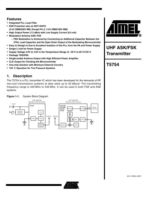
1. Description<br />
The <strong>T5754</strong> is a PLL transmitter IC which has been developed for the demands of RF<br />
low-cost transmission systems at data rates up to 32 kBaud. The transmitting<br />
frequency range is 429 MHz to 439 MHz. It can be used in both <strong>FSK</strong> and <strong>ASK</strong><br />
systems.<br />
Figure 1-1.<br />
System Block Diagram<br />
1 Li cell<br />
Keys<br />
Encoder<br />
ATARx9x<br />
<strong>UHF</strong> <strong>ASK</strong>/<strong>FSK</strong><br />
Remote control transmitter<br />
<strong>T5754</strong><br />
PLL<br />
U3741B/<br />
U3745B/<br />
T5743/<br />
T5744<br />
<strong>UHF</strong> <strong>ASK</strong>/<strong>FSK</strong><br />
Remote control receiver<br />
Demod<br />
Control<br />
1 to 3<br />
Microcontroller<br />
Antenna<br />
Antenna<br />
XTO<br />
VCO<br />
PLL<br />
XTO<br />
Power<br />
amp.<br />
LNA<br />
VCO<br />
4511I–RKE–02/07
2. Pin Configuration<br />
Figure 2-1.<br />
Pinning TSSOP8L<br />
CLK<br />
PA_ENABLE<br />
ANT2<br />
ANT1<br />
1<br />
2<br />
3<br />
4<br />
8<br />
7<br />
6<br />
5<br />
ENABLE<br />
GND<br />
VS<br />
XTAL<br />
Table 2-1.<br />
Pin Description<br />
Pin Symbol Function Configuration<br />
VS<br />
1 CLK<br />
Clock output signal for micro con roller<br />
The clock output frequency is set by the<br />
crystal to f XTAL /4<br />
100Ω<br />
CLK<br />
100Ω<br />
2 PA_ENABLE<br />
Switches on power amplifier, used for<br />
<strong>ASK</strong> modulation<br />
PA_ENABLE<br />
50 kΩ<br />
U REF = 1.1V<br />
20 µA<br />
ANT1<br />
3<br />
ANT2<br />
Emitter of antenna output stage<br />
4<br />
ANT1<br />
Open collector antenna output<br />
ANT2<br />
2<br />
<strong>T5754</strong><br />
4511I–RKE–02/07
<strong>T5754</strong><br />
Table 2-1.<br />
Pin Description (Continued)<br />
Pin Symbol Function Configuration<br />
VS<br />
VS<br />
1.5 kΩ 1.2 kΩ<br />
5 XTAL Connection for crystal<br />
XTAL<br />
182 µA<br />
6 VS Supply voltage See ESD protection circuitry (see Figure 4-5 on page 9)<br />
7 GND Ground See ESD protection circuitry (see Figure 4-5 on page 9)<br />
8 ENABLE Enable input<br />
ENABLE<br />
200 kΩ<br />
Figure 2-2.<br />
Block Diagram<br />
<strong>T5754</strong><br />
Power up/down<br />
CLK<br />
1<br />
f<br />
4<br />
8<br />
ENABLE<br />
f<br />
32<br />
PA_ENABLE<br />
2<br />
PDF<br />
7<br />
GND<br />
CP<br />
ANT2<br />
3<br />
6<br />
VS<br />
LF<br />
ANT1<br />
4<br />
PA<br />
PLL<br />
VCO<br />
XTO<br />
5<br />
XTAL<br />
3<br />
4511I–RKE–02/07
3. General Description<br />
4. Functional Description<br />
This fully integrated PLL transmitter allows particularly simple, low-cost RF miniature transmitters<br />
to be assembled. The VCO is locked to 32 f XTAL hence a 13.56 MHz crystal is needed for a<br />
433.92 MHz transmitter. All other PLL and VCO peripheral elements are integrated.<br />
The XTO is a series resonance oscillator so that only one capacitor together with a crystal connected<br />
in series to GND are needed as external elements.<br />
The crystal oscillator together with the PLL needs typically < 1 ms until the PLL is locked and the<br />
CLK output is stable. There is a wait time of ≥ 1 ms until the CLK is used for the microcontroller<br />
and the PA is switched on.<br />
The power amplifier is an open-collector output delivering a current pulse which is nearly independent<br />
from the load impedance. The delivered output power is hence controllable via the<br />
connected load impedance.<br />
This output configuration enables a simple matching to any kind of antenna or to 50Ω. A high<br />
power efficiency of η= P out /(I S,PA V S ) of 36% for the power amplifier results when an optimized<br />
load impedance of Z Load = (166 + j223)Ω is used at 3V supply voltage.<br />
If ENABLE = L and the PA_ENABLE = L, the circuit is in standby mode consuming only a very<br />
small amount of current so that a lithium cell used as power supply can work for several years.<br />
With ENABLE = H the XTO, PLL and the CLK driver are switched on. If PA_ENABLE remains L<br />
only the PLL and the XTO is running and the CLK signal is delivered to the microcontroller. The<br />
VCO locks to 32 times the XTO frequency.<br />
With ENABLE = H and PA_ENABLE = H the PLL, XTO, CLK driver and the power amplifier are<br />
on. With PA_ENABLE the power amplifier can be switched on and off, which is used to perform<br />
the <strong>ASK</strong> modulation.<br />
4.1 <strong>ASK</strong> Transmission<br />
The <strong>T5754</strong> is activated by ENABLE = H. PA_ENABLE must remain L for t ≥1 ms, then the CLK<br />
signal can be taken to clock the microcontroller and the output power can be modulated by<br />
means of pin PA_ENABLE. After transmission PA_ENABLE is switched to L and the microcontroller<br />
switches back to internal clocking. The <strong>T5754</strong> is switched back to standby mode with<br />
ENABLE = L.<br />
4.2 <strong>FSK</strong> Transmission<br />
The <strong>T5754</strong> is activated by ENABLE = H. PA_ENABLE must remain L for t ≥1 ms, then the CLK<br />
signal can be taken to clock the microcontroller and the power amplifier is switched on with<br />
PA_ENABLE = H. The chip is then ready for <strong>FSK</strong> modulation. The microcontroller starts to<br />
switch on and off the capacitor between the XTAL load capacitor and GND with an open-drain<br />
output port, thus changing the reference frequency of the PLL. If the switch is closed, the output<br />
frequency is lower than if the switch is open. After transmission PA_ENABLE is switched to L<br />
and the microcontroller switches back to internal clocking. The <strong>T5754</strong> is switched back to<br />
standby mode with ENABLE = L.<br />
The accuracy of the frequency deviation with XTAL pulling method is about ±25% when the following<br />
tolerances are considered.<br />
4<br />
<strong>T5754</strong><br />
4511I–RKE–02/07
<strong>T5754</strong><br />
Figure 4-1.<br />
Tolerances of Frequency Modulation<br />
V S<br />
XTAL<br />
C Stray1<br />
C M<br />
C Stray2<br />
L M C 4<br />
R S<br />
C 0 C 5<br />
C Switch<br />
Crystal equivalent circuit<br />
Using C 4 =9.2pF±2%, C 5 = 6.8 pF ±5%, a switch port with C Switch = 3 pF ±10%, stray capacitances<br />
on each side of the crystal of C Stray1 =C Stray2 = 1 pF ±10%, a parallel capacitance of the<br />
crystal of C 0 = 3.2 pF ±10% and a crystal with C M = 13 fF ±10%, an <strong>FSK</strong> deviation of ±21 kHz<br />
typical with worst case tolerances of ±16.3 kHz to ±28.8 kHz results.<br />
4.3 CLK Output<br />
An output CLK signal is provided for a connected microcontroller, the delivered signal is CMOS<br />
compatible if the load capacitance is lower than 10 pF.<br />
4.3.1 Clock Pulse Take-over<br />
The clock of the crystal oscillator can be used for clocking the microcontroller. Atmel ® ’s<br />
ATARx9x has the special feature of starting with an integrated RC-oscillator to switch on the<br />
<strong>T5754</strong> with ENABLE = H, and after 1 ms to assume the clock signal of the transmission IC, so<br />
that the message can be sent with crystal accuracy.<br />
4.3.2 Output Matching and Power Setting<br />
The output power is set by the load impedance of the antenna. The maximum output power is<br />
achieved with a load impedance of Z Load,opt = (166 + j223)Ω. There must be a low resistive path<br />
to V S to deliver the DC current.<br />
The delivered current pulse of the power amplifier is 9 mA and the maximum output power is<br />
delivered to a resistive load of 465Ω if the 1.0 pF output capacitance of the power amplifier is<br />
compensated by the load impedance.<br />
An optimum load impedance of:<br />
Z Load =465Ω || j/(2 ×π1.0pF)=(166+j223)Ω thus results for the maximum output power of<br />
7.5 dBm.<br />
The load impedance is defined as the impedance seen from the <strong>T5754</strong>’s ANT1, ANT2 into the<br />
matching network. Do not confuse this large signal load impedance with a small signal input<br />
impedance delivered as input characteristic of RF amplifiers and measured from the application<br />
into the IC instead of from the IC into the application for a power amplifier.<br />
Less output power is achieved by lowering the real parallel part of 465Ω where the parallel imaginary<br />
part should be kept constant.<br />
Output power measurement can be done with the circuit of Figure 4-2 on page 6. Note that the<br />
component values must be changed to compensate the individual board parasitics until the<br />
<strong>T5754</strong> has the right load impedance Z Load,opt = (166 + j223)Ω. Also the damping of the cable<br />
used to measure the output power must be calibrated out.<br />
4511I–RKE–02/07<br />
5
Figure 4-2.<br />
Output Power Measurement<br />
V S<br />
C 1<br />
1 nF<br />
ANT1<br />
L 1<br />
Z Lopt<br />
33 nH<br />
C 2<br />
2.2 pF<br />
Z = 50Ω<br />
Power<br />
meter<br />
R in<br />
50Ω<br />
ANT2<br />
4.4 Application Circuit<br />
For the supply-voltage blocking capacitor C 3 a value of 68 nF/X7R is recommended (see Figure<br />
4-3 on page 7 and Figure 4-4 on page 8). C 1 and C 2 are used to match the loop antenna to the<br />
power amplifier where C 1 typically is 8.2 pF/NP0 and C 2 is 6 pF/NP0 (10 pF + 15 pF in series);<br />
for C 2 two capacitors in series should be used to achieve a better tolerance value and to have<br />
the possibility to realize the Z Load,opt by using standard valued capacitors.<br />
C 1 forms together with the pins of <strong>T5754</strong> and the PCB board wires a series resonance loop that<br />
suppresses the 1 st harmonic, hence the position of C 1 on the PCB is important. Normally the<br />
best suppression is achieved when C 1 is placed as close as possible to the pins ANT1 and<br />
ANT2.<br />
The loop antenna should not exceed a width of 1.5 mm, otherwise the Q-factor of the loop<br />
antenna is too high.<br />
L 1 ([50 nH to 100 nH) can be printed on PCB. C 4 should be selected that the XTO runs on the<br />
load resonance frequency of the crystal. Normally, a value of 12 pF results for a 15 pF<br />
load-capacitance crystal.<br />
6<br />
<strong>T5754</strong><br />
4511I–RKE–02/07
7<br />
4511I–RKE–02/07<br />
<strong>T5754</strong><br />
Figure 4-3.<br />
<strong>ASK</strong> Application Circuit<br />
ATARx9x<br />
<strong>T5754</strong><br />
CP<br />
Power up/down<br />
PDF<br />
32<br />
5<br />
6<br />
7<br />
1<br />
VDD<br />
BPXY<br />
20<br />
VSS<br />
VS<br />
8<br />
4<br />
3<br />
2<br />
XTAL<br />
XTAL<br />
VS<br />
VS<br />
VS<br />
GND<br />
ENABLE<br />
ANT1<br />
L1<br />
C1<br />
C4<br />
C3<br />
Loop<br />
Antenna<br />
C2<br />
ANT2<br />
PA_ENABLE<br />
OSC1<br />
BPXY<br />
BPXY<br />
BPXY<br />
S1<br />
S2<br />
7<br />
CLK<br />
1<br />
f<br />
LF<br />
PA<br />
VCO<br />
PLL<br />
XTO<br />
4<br />
f
8<br />
4511I–RKE–02/07<br />
<strong>T5754</strong><br />
Figure 4-4.<br />
<strong>FSK</strong> Application Circuit<br />
ATARx9x<br />
<strong>T5754</strong><br />
CP<br />
Power up/down<br />
PDF<br />
32<br />
5<br />
6<br />
7<br />
1<br />
VDD<br />
BPXY<br />
20<br />
VSS<br />
VS<br />
8<br />
4<br />
3<br />
2<br />
XTAL<br />
XTAL<br />
VS<br />
VS<br />
VS<br />
GND<br />
ENABLE<br />
ANT1<br />
L1<br />
C1<br />
C5<br />
C4<br />
C3<br />
Loop<br />
Antenna<br />
C2<br />
ANT2<br />
PA_ENABLE<br />
OSC1<br />
BPXY<br />
BPXY<br />
BPXY<br />
S1<br />
S2<br />
7<br />
CLK<br />
1<br />
f<br />
LF<br />
PA<br />
VCO<br />
PLL<br />
XTO<br />
4<br />
f<br />
18<br />
BP42/T2O
<strong>T5754</strong><br />
Figure 4-5.<br />
ESD Protection Circuit<br />
VS<br />
ANT1<br />
CLK<br />
PA_ENABLE<br />
ANT2<br />
XTAL<br />
ENABLE<br />
GND<br />
5. Absolute Maximum Ratings<br />
Stresses beyond those listed under “Absolute Maximum Ratings” may cause permanent damage to the device. This is a stress rating<br />
only and functional operation of the device at these or any other conditions beyond those indicated in the operational sections of this<br />
specification is not implied. Exposure to absolute maximum rating conditions for extended periods may affect device reliability.<br />
Parameters Symbol Minimum Maximum Unit<br />
Supply voltage V S 5 V<br />
Power dissipation P tot 100 mW<br />
Junction temperature T j 150 °C<br />
Storage temperature T stg –55 125 °C<br />
Ambient temperature T amb –55 125 °C<br />
Input voltage V maxPA_ENABLE –0.3 (V S + 0.3) (1) V<br />
Note: 1. If V S + 0.3 is higher than 3.7V, the maximum voltage will be reduced to 3.7V.<br />
6. Thermal Resistance<br />
Parameters Symbol Value Unit<br />
Junction ambient R thJA 170 K/W<br />
7. Electrical Characteristics<br />
V S = 2.0V to 4.0V, T amb = –40°C to 125°C unless otherwise specified.<br />
Typical values are given at V S = 3.0 V and T amb = 25°C. All parameters are referred to GND (pin 7).<br />
Parameters Test Conditions Symbol Min. Typ. Max. Unit<br />
Supply current<br />
Supply current<br />
Supply current<br />
Power down<br />
V ENABLE < 0.25V, –40°C to 85°C<br />
V PA-ENABLE < 0.25V, –40°C to +125°C<br />
V PA-ENABLE < 0.25V, 25°C<br />
(100% correlation tested)<br />
Power up, PA off, V S = 3V,<br />
V ENABLE >1.7V, V PA-ENABLE < 0.25V<br />
Power up, V S = 3.0V,<br />
V ENABLE >1.7V, V PA-ENABLE >1.7V<br />
I S_Off<br />
< 10<br />
350<br />
7<br />
nA<br />
µA<br />
nA<br />
I S 3.7 4.8 mA<br />
I S_Transmit 9 11.6 mA<br />
V<br />
Output power<br />
S = 3.0V, T amb =25°C,<br />
P<br />
f = 433.92 MHz, Z Load = (166 + j233)Ω<br />
Ref 5.5 7.5 10 dBm<br />
Note: 1. If V S is higher than 3.6V, the maximum voltage will be reduced to 3.6V.<br />
4511I–RKE–02/07<br />
9
7. Electrical Characteristics (Continued)<br />
V S = 2.0V to 4.0V, T amb = –40°C to 125°C unless otherwise specified.<br />
Typical values are given at V S = 3.0 V and T amb = 25°C. All parameters are referred to GND (pin 7).<br />
Parameters Test Conditions Symbol Min. Typ. Max. Unit<br />
Output power variation for the full<br />
temperature range<br />
Output power variation for the full<br />
temperature range<br />
T amb = –40°C to +85°C,<br />
V S = 3.0V<br />
V S = 2.0V<br />
T amb = –40°C to +125°C,<br />
V S = 3.0V<br />
V S = 2.0V<br />
P Out = P Ref + ∆P Ref<br />
∆P Ref<br />
∆P Ref<br />
–1.5<br />
–4.0<br />
∆P Ref<br />
–2.0<br />
∆P Ref –4.5<br />
Achievable output-power range Selectable by load impedance P Out_typ 0 7.5 dBm<br />
Spurious emission<br />
Oscillator frequency XTO<br />
(= phase comparator frequency)<br />
f CLK = f 0 /128<br />
Load capacitance at pin CLK = 10 pF<br />
f O ±1 × f CLK<br />
f O ±4 × f CLK<br />
other spurious are lower<br />
f XTO = f 0 /32<br />
f XTAL = resonant frequency of the XTAL,<br />
C M ≤ 10 fF, load capacitance selected<br />
accordingly<br />
T amb = –40°C to +85°C<br />
T amb = –40°C to +125°C<br />
f XTO<br />
–30<br />
–40<br />
–55<br />
–52<br />
f XTAL +30<br />
+40<br />
PLL loop bandwidth 250 kHz<br />
Phase noise of phase comparator<br />
Referred to f PC = f XT0,<br />
25 kHz distance to carrier<br />
–116 –110 dBc/Hz<br />
In loop phase noise PLL 25 kHz distance to carrier –86 –80 dBc/Hz<br />
Phase noise VCO<br />
at 1 MHz<br />
at 36 MHz<br />
–94<br />
–125<br />
–90<br />
–121<br />
dB<br />
dB<br />
dB<br />
dB<br />
dBc<br />
dBc<br />
ppm<br />
ppm<br />
dBc/Hz<br />
dBc/Hz<br />
Frequency range of VCO f VCO 429 439 MHz<br />
Clock output frequency (CMOS<br />
f<br />
microcontroller compatible)<br />
0 /128<br />
MHz<br />
Voltage swing at pin CLK C Load ≤10 pF<br />
V 0h V S × 0.8<br />
V<br />
V 0l V S × 0.2 V<br />
Series resonance R of the crystal Rs 110 Ω<br />
Capacitive load at pin XT0 7 pF<br />
<strong>FSK</strong> modulation frequency rate Duty cycle of the modulation signal = 50% 0 32 kHz<br />
<strong>ASK</strong> modulation frequency rate Duty cycle of the modulation signal = 50% 0 32 kHz<br />
ENABLE input<br />
PA_ENABLE input<br />
Low level input voltage<br />
High level input voltage<br />
Input current high<br />
Low level input voltage<br />
High level input voltage<br />
Input current high<br />
Note: 1. If V S is higher than 3.6V, the maximum voltage will be reduced to 3.6V.<br />
V Il<br />
V Ih<br />
I In<br />
1.7<br />
V Il<br />
V Ih<br />
I In<br />
1.7<br />
0.25<br />
20<br />
0.25<br />
V S<br />
(1)<br />
5<br />
V<br />
V<br />
µA<br />
V<br />
V<br />
µA<br />
10<br />
<strong>T5754</strong><br />
4511I–RKE–02/07
<strong>T5754</strong><br />
8. Ordering Information<br />
Extended Type Number Package Remarks<br />
<strong>T5754</strong>-6AQJ TSSOP8L Taped and reeled, Marking: T574, Pb-free<br />
<strong>T5754</strong>-6APJ TSSOP8L Taped and reeled, Marking: T574, small reel, Pb-free<br />
9. Package Information<br />
Package: TSSOP 8L<br />
Dimensions in mm<br />
+0.05<br />
1-0.15<br />
0.85±0.05<br />
3±0.1<br />
3±0.1<br />
+0.06<br />
0.31-0.07<br />
0.65 nom.<br />
0.1±0.05<br />
3.8±0.3<br />
4.9±0.1<br />
+0.05<br />
0.15-0.02<br />
3 x 0.65 = 1.95 nom.<br />
8 5<br />
technical drawings<br />
according to DIN<br />
specifications<br />
Drawing-No.: 6.543-5083.01-4<br />
Issue: 2; 15.03.04<br />
1 4<br />
4511I–RKE–02/07<br />
11
10. Revision History<br />
Please note that the following page numbers referred to in this section refer to the specific revision<br />
mentioned, not to this document.<br />
Revision No. History<br />
4711I-RKE-02/07<br />
4711H-RKE-09/05<br />
4711G-RKE-05/05<br />
4711F-RKE-07/04<br />
• Put datasheet in a new template<br />
• Pb-free logo on page 1 deleted<br />
• Pb-free logo on page 1 added<br />
• Ordering Information on page 11 changed<br />
• Put datasheet in a new template<br />
• Package Information (page 11): Replace old package drawing through current<br />
version<br />
• Abs. Max. Ratings table (page 9): row “Input voltage” added<br />
• Abs. Max. Ratings table (page 9): table note 1 added<br />
• El. Char. table (pages 9 to 10): row “PA_ENABLE input“ changed<br />
• El. Char. table (pages 9 to 10): table note 1 added<br />
• Ordering Information table (page 11): Remarks changed<br />
12<br />
<strong>T5754</strong><br />
4511I–RKE–02/07
Atmel Corporation<br />
2325 Orchard Parkway<br />
San Jose, CA 95131, USA<br />
Tel: 1(408) 441-0311<br />
Fax: 1(408) 487-2600<br />
Regional Headquarters<br />
Europe<br />
Atmel Sarl<br />
Route des Arsenaux 41<br />
Case Postale 80<br />
CH-1705 Fribourg<br />
Switzerland<br />
Tel: (41) 26-426-5555<br />
Fax: (41) 26-426-5500<br />
Asia<br />
Room 1219<br />
Chinachem Golden Plaza<br />
77 Mody Road Tsimshatsui<br />
East Kowloon<br />
Hong Kong<br />
Tel: (852) 2721-9778<br />
Fax: (852) 2722-1369<br />
Japan<br />
9F, Tonetsu Shinkawa Bldg.<br />
1-24-8 Shinkawa<br />
Chuo-ku, Tokyo 104-0033<br />
Japan<br />
Tel: (81) 3-3523-3551<br />
Fax: (81) 3-3523-7581<br />
Atmel Operations<br />
Memory<br />
2325 Orchard Parkway<br />
San Jose, CA 95131, USA<br />
Tel: 1(408) 441-0311<br />
Fax: 1(408) 436-4314<br />
Microcontrollers<br />
2325 Orchard Parkway<br />
San Jose, CA 95131, USA<br />
Tel: 1(408) 441-0311<br />
Fax: 1(408) 436-4314<br />
La Chantrerie<br />
BP 70602<br />
44306 Nantes Cedex 3, France<br />
Tel: (33) 2-40-18-18-18<br />
Fax: (33) 2-40-18-19-60<br />
ASIC/ASSP/Smart Cards<br />
Zone Industrielle<br />
13106 Rousset Cedex, France<br />
Tel: (33) 4-42-53-60-00<br />
Fax: (33) 4-42-53-60-01<br />
1150 East Cheyenne Mtn. Blvd.<br />
Colorado Springs, CO 80906, USA<br />
Tel: 1(719) 576-3300<br />
Fax: 1(719) 540-1759<br />
Scottish Enterprise Technology Park<br />
Maxwell Building<br />
East Kilbride G75 0QR, Scotland<br />
Tel: (44) 1355-803-000<br />
Fax: (44) 1355-242-743<br />
RF/Automotive<br />
Theresienstrasse 2<br />
Postfach 3535<br />
74025 Heilbronn, Germany<br />
Tel: (49) 71-31-67-0<br />
Fax: (49) 71-31-67-2340<br />
1150 East Cheyenne Mtn. Blvd.<br />
Colorado Springs, CO 80906, USA<br />
Tel: 1(719) 576-3300<br />
Fax: 1(719) 540-1759<br />
Biometrics<br />
Avenue de Rochepleine<br />
BP 123<br />
38521 Saint-Egreve Cedex, France<br />
Tel: (33) 4-76-58-47-50<br />
Fax: (33) 4-76-58-47-60<br />
Literature Requests<br />
www.atmel.com/literature<br />
Disclaimer: The information in this document is provided in connection with Atmel products. No license, express or implied, by estoppel or otherwise, to any<br />
intellectual property right is granted by this document or in connection with the sale of Atmel products. EXCEPT AS SET FORTH IN ATMEL’S TERMS AND CONDI-<br />
TIONS OF SALE LOCATED ON ATMEL’S WEB SITE, ATMEL ASSUMES NO LIABILITY WHATSOEVER AND DISCLAIMS ANY EXPRESS, IMPLIED OR STATUTORY<br />
WARRANTY RELATING TO ITS PRODUCTS INCLUDING, BUT NOT LIMITED TO, THE IMPLIED WARRANTY OF MERCHANTABILITY, FITNESS FOR A PARTICULAR<br />
PURPOSE, OR NON-INFRINGEMENT. IN NO EVENT SHALL ATMEL BE LIABLE FOR ANY DIRECT, INDIRECT, CONSEQUENTIAL, PUNITIVE, SPECIAL OR INCIDEN-<br />
TAL DAMAGES (INCLUDING, WITHOUT LIMITATION, DAMAGES FOR LOSS OF PROFITS, BUSINESS INTERRUPTION, OR LOSS OF INFORMATION) ARISING OUT<br />
OF THE USE OR INABILITY TO USE THIS DOCUMENT, EVEN IF ATMEL HAS BEEN ADVISED OF THE POSSIBILITY OF SUCH DAMAGES. Atmel makes no<br />
representations or warranties with respect to the accuracy or completeness of the contents of this document and reserves the right to make changes to specifications<br />
and product descriptions at any time without notice. Atmel does not make any commitment to update the information contained herein. Unless specifically provided<br />
otherwise, Atmel products are not suitable for, and shall not be used in, automotive applications. Atmel’s products are not intended, authorized, or warranted for use<br />
as components in applications intended to support or sustain life.<br />
© 2007 Atmel Corporation. All rights reserved. Atmel ® , logo and combinations thereof, Everywhere You Are ® and others are registered trademarks<br />
or trademarks of Atmel Corporation or its subsidiaries. Other terms and product names may be trademarks of others.<br />
4511I–RKE–02/07