
You also want an ePaper? Increase the reach of your titles
YUMPU automatically turns print PDFs into web optimized ePapers that Google loves.
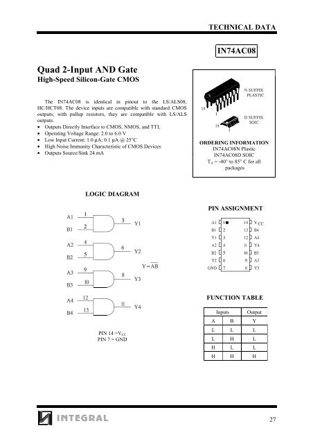
TECHNICAL DATA<br />
<strong>IN74AC08</strong><br />
Quad 2-Input AND Gate<br />
High-Speed Silicon-Gate CMOS<br />
The <strong>IN74AC08</strong> is identical in pinout to the LS/ALS08,<br />
HC/HCT08. The device inputs are compatible with standard CMOS<br />
outputs; with pullup resistors, they are compatible with LS/ALS<br />
outputs.<br />
• Outputs Directly Interface to CMOS, NMOS, and TTL<br />
• Operating Voltage Range: 2.0 to 6.0 V<br />
• Low Input Current: 1.0 µA; 0.1 µA @ 25°C<br />
• High Noise Immunity Characteristic of CMOS Devices<br />
• Outputs Source/Sink 24 mA<br />
ORDERING INFORMATION<br />
<strong>IN74AC08</strong>N Plastic<br />
<strong>IN74AC08</strong>D SOIC<br />
T A = -40° to 85° C for all<br />
packages<br />
LOGIC DIAGRAM<br />
PIN ASSIGNMENT<br />
FUNCTION TABLE<br />
PIN 14 =V CC<br />
PIN 7 = GND<br />
Inputs Output<br />
A B Y<br />
L L L<br />
L H L<br />
H L L<br />
H H H<br />
27
<strong>IN74AC08</strong><br />
MAXIMUM RATINGS *<br />
Symbol Parameter Value Unit<br />
V CC DC Supply Voltage (Referenced to GND) -0.5 to +7.0 V<br />
V IN DC Input Voltage (Referenced to GND) -0.5 to V CC +0.5 V<br />
V OUT DC Output Voltage (Referenced to GND) -0.5 to V CC +0.5 V<br />
I IN DC Input Current, per Pin ±20 mA<br />
I OUT DC Output Sink/Source Current, per Pin ±50 mA<br />
I CC DC Supply Current, V CC and GND Pins ±50 mA<br />
P D<br />
Power Dissipation in Still Air, Plastic DIP+<br />
SOIC Package+<br />
Tstg Storage Temperature -65 to +150 °C<br />
T L<br />
Lead Temperature, 1 mm from Case for 10 Seconds<br />
(Plastic DIP or SOIC Package)<br />
750<br />
500<br />
* Maximum Ratings are those values beyond which damage to the device may occur.<br />
Functional operation should be restricted to the Recommended Operating Conditions.<br />
+Derating - Plastic DIP: - 10 mW/°C from 65° to 125°C<br />
SOIC Package: : - 7 mW/°C from 65° to 125°C<br />
mW<br />
260 °C<br />
RECOMMENDED OPERATING CONDITIONS<br />
Symbol Parameter Min Max Unit<br />
V CC DC Supply Voltage (Referenced to GND) 2.0 6.0 V<br />
V IN , V OUT DC Input Voltage, Output Voltage (Referenced to GND) 0 V CC V<br />
T J Junction Temperature (PDIP) 140 °C<br />
T A Operating Temperature, All Package Types -40 +85 °C<br />
I OH Output Current - High -24 mA<br />
I OL Output Current - Low 24 mA<br />
t r , t f Input Rise and Fall Time *<br />
(except Schmitt Inputs)<br />
*<br />
V IN from 30% to 70% V CC<br />
V CC =3.0 V<br />
V CC =4.5 V<br />
V CC =5.5 V<br />
0<br />
0<br />
0<br />
150<br />
40<br />
25<br />
ns/V<br />
This device contains protection circuitry to guard against damage due to high static voltages or electric<br />
fields. However, precautions must be taken to avoid applications of any voltage higher than maximum rated<br />
voltages to this high-impedance circuit. For proper operation, V IN and V OUT should be constrained to the range<br />
GND≤(V IN or V OUT )≤V CC .<br />
Unused inputs must always be tied to an appropriate logic voltage level (e.g., either GND or V CC ).<br />
Unused outputs must be left open.<br />
28
<strong>IN74AC08</strong><br />
DC ELECTRICAL CHARACTERISTICS(Voltages Referenced to GND)<br />
V CC Guaranteed Limits<br />
Symbol Parameter Test Conditions V 25 °C -40°C to<br />
85°C<br />
V IH<br />
Minimum High-Level<br />
Input Voltage<br />
V IL Maximum Low -<br />
Level Input Voltage<br />
V OH<br />
Minimum High-Level<br />
Output Voltage<br />
V OUT =0.1 V or V CC -0.1 V 3.0<br />
4.5<br />
5.5<br />
V OUT =0.1 V 3.0<br />
4.5<br />
5.5<br />
I OUT ≤ -50 µA 3.0<br />
4.5<br />
5.5<br />
2.1<br />
3.15<br />
3.85<br />
0.9<br />
1.35<br />
1.65<br />
2.9<br />
4.4<br />
5.4<br />
2.1<br />
3.15<br />
3.85<br />
0.9<br />
1.35<br />
1.65<br />
2.9<br />
4.4<br />
5.4<br />
Unit<br />
V<br />
V<br />
V<br />
* V IN = V IH<br />
I OH =-12 mA<br />
I OH =-24 mA<br />
I OH =-24 mA<br />
3.0<br />
4.5<br />
5.5<br />
2.56<br />
3.86<br />
4.86<br />
2.46<br />
3.76<br />
4.76<br />
V OL<br />
Maximum Low-Level<br />
Output Voltage<br />
I OUT ≤ 50 µA 3.0<br />
4.5<br />
5.5<br />
0.1<br />
0.1<br />
0.1<br />
0.1<br />
0.1<br />
0.1<br />
V<br />
I IN<br />
I OLD<br />
I OHD<br />
Maximum Input<br />
Leakage Current<br />
+Minimum Dynamic<br />
Output Current<br />
+Minimum Dynamic<br />
Output Current<br />
* V IN = V IL or V IH<br />
I OL =12 mA<br />
I OL =24 mA<br />
I OL =24 mA<br />
3.0<br />
4.5<br />
5.5<br />
0.36<br />
0.36<br />
0.36<br />
0.44<br />
0.44<br />
0.44<br />
V IN =V CC or GND 5.5 ±0.1 ±1.0 µA<br />
V OLD =1.65 V Max 5.5 75 mA<br />
V OHD =3.85 V Min 5.5 -75 mA<br />
I CC Maximum Quiescent V IN =V CC or GND 5.5 4.0 40 µA<br />
Supply Current<br />
(per Package)<br />
*<br />
All outputs loaded; thresholds on input associated with output under test.<br />
+Maximum test duration 2.0 ms, one output loaded at a time.<br />
Note: I IN and I CC @ 3.0 V are guaranteed to be less than or equal to the respective limit @ 5.5 V V CC<br />
29
<strong>IN74AC08</strong><br />
AC ELECTRICAL CHARACTERISTICS(C L =50pF,Input t r =t f =3.0 ns)<br />
V CC<br />
*<br />
Guaranteed Limits<br />
Symbol Parameter V 25 °C -40°C to<br />
85°C<br />
t PLH<br />
t PHL<br />
Propagation Delay, Input A or B to<br />
Output Y (Figure 1)<br />
Propagation Delay, Input A or B to<br />
Output Y (Figure 1)<br />
3.3<br />
5.0<br />
Min Max Min Max<br />
C IN Maximum Input Capacitance 5.0 4.5 4.5 pF<br />
3.3<br />
5.0<br />
1.5<br />
1.5<br />
1.5<br />
1.5<br />
9.5<br />
7.5<br />
8.5<br />
7.0<br />
1.0<br />
1.0<br />
1.0<br />
1.0<br />
10.0<br />
8.5<br />
9.0<br />
7.5<br />
Unit<br />
ns<br />
ns<br />
Typical @25°C,V CC =5.0 V<br />
C PD Power Dissipation Capacitance 20 pF<br />
* Voltage Range 3.3 V is 3.3 V ±0.3 V<br />
Voltage Range 5.0 V is 5.0 V ±0.5 V<br />
Figure 1. Switching Waveforms<br />
30