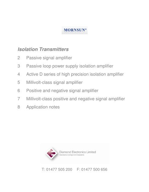
Isolation Transmitters
Isolation Transmitters
Isolation Transmitters

Create successful ePaper yourself
Turn your PDF publications into a flip-book with our unique Google optimized e-Paper software.
<strong>Isolation</strong> <strong>Transmitters</strong><br />
2 Passive signal amplifier<br />
3 Passive loop power supply isolation amplifier<br />
4 Active D series of high precision isolation amplifier<br />
5 Millivolt-class signal amplifier<br />
6 Positive and negative signal amplifier<br />
7 Millivolt-class positive and negative signal amplifier<br />
8 Application notes<br />
T: 01477 505 200 F: 01477 500 656
E: sales@diamondelec.co.uk W: www.diamondelec.co.uk
IGBT Drive Special Power<br />
<strong>Isolation</strong> Amplifier Module<br />
QA01, QA02, QA03, QA04<br />
Specially Designed For IGBT Driver<br />
DC-DC Converter<br />
QA01,QA02,QA03 ,QA04 are specially designed for the<br />
IGBT driver which needs two isolation power supply. With<br />
two independent outputs, it can be better to supply power<br />
to the ON/OFF driver. The module also provides functions<br />
of short circuit protection and self-recovery capability.<br />
FEATURES<br />
Input voltage range:As table<br />
Miniature size, Light weight<br />
3000VAC isolation(input,output;Tested for 1min/1mA)<br />
Short circuit protection<br />
SPECIFICATIONS<br />
Operating temperature.....................-40℃~+85℃(QA01,QA02,QA03)<br />
Efficiency.........................................80%<br />
-40℃~+105℃(QA04)<br />
Input voltage range...................................QA01: 14.5~15.5VDC<br />
QA02: 11.6~12.4VDC<br />
QA03: 23.3~24.7VDC<br />
QA04: 9~15VDC<br />
Line regulation(Vin change of 1%).....1.5%(max)(QA01,QA02,QA03)<br />
Size: 19.5x9.8x12.5(mm)<br />
3.20<br />
(0.126)<br />
VIN<br />
12.5<br />
(0.492)<br />
(0.161)<br />
6<br />
(0.079)<br />
19.5(0.768)<br />
C1 +<br />
0.50<br />
(0.020)<br />
(0.100) (0.020)<br />
Note:First angle projection<br />
TEST EXAMPLE<br />
Q A W X C X X D - X X<br />
100μF/35V<br />
1<br />
(0.386)<br />
QA0x<br />
Special output label<br />
Package marking<br />
Product serial number<br />
Number of output groups<br />
Representative voltage input type<br />
Dedicated power supply for IGBT Driver<br />
RECOMMENDED FOOTPRINT<br />
Top View,grid: 2.54mm(0. 1inch)<br />
1.00 [0.039]<br />
Pin Function<br />
1<br />
2<br />
5<br />
6<br />
7<br />
7<br />
C2 +<br />
100μF/35V<br />
6<br />
V<br />
A<br />
6<br />
Vin<br />
GND<br />
-Vo<br />
0V(com)<br />
+Vo<br />
Load<br />
Passive Signal Amplifier<br />
T1100 series, a standard analog amplifier, with 4-20mA current signal input<br />
and 4-20mA current signal output, is a passive signal isolation module.<br />
Adopting unique electromagnetism isolation design and high efficiency loop<br />
electric-larceny technology, independent power supply isn’t required for the<br />
module, realizing 4-20mA standard signal isolation with high accuracy and<br />
linearity. Besides, the modules have extremely low temperature drift (no<br />
more than 35ppm/℃under -25 ℃ ~ +71 ℃ ). The isolation voltage between the<br />
input and output can be up to 3KVDC.<br />
T1100N/NS PACKAGE INFORMATION AND PIN ASSIGNMENT<br />
T1100RN/N<br />
2.54<br />
[0.100]<br />
1.50<br />
(0.059)<br />
23.80[0.937]<br />
17.78<br />
[0.700]<br />
0.50<br />
[0.020]<br />
(DIP Package)<br />
8.00[0.315]<br />
0.50<br />
[0.020]<br />
13.70[0.539]<br />
Note:First angle projection<br />
1 2 9 101112<br />
32.00(1.260)<br />
0.80<br />
[0.031]<br />
T1100RNS/NS<br />
7.90<br />
(0.311)<br />
23.80[0.937]<br />
17.78<br />
[0.700]<br />
(SMD Package)<br />
8.00[0.315]<br />
0.50<br />
[0.020]<br />
18.60<br />
[0.737]<br />
PIN<br />
1(Sout-)<br />
2(Sout+)<br />
7(Sin+)<br />
8(Sin-)<br />
Others<br />
T1100L PACKAGE INFORMATION AND PIN ASSIGNMENT<br />
Signal<br />
output<br />
1 2 9 101112<br />
NC<br />
NC<br />
NC<br />
2.54<br />
NC<br />
NC<br />
2( Iin-)<br />
Sout-<br />
Sout+<br />
NC<br />
Sin+<br />
Sin-<br />
Signal<br />
input<br />
2.54<br />
NC: No Connection, otherwise the<br />
module will be damaged.<br />
Unit: mm<br />
Tolerance: 0.0±0.25,0.00±0.25<br />
PIN<br />
1( Iin+ )<br />
FUNCTION<br />
Signal Output-<br />
Signal Output+<br />
Signal Input+<br />
Signal Input-<br />
NC<br />
FUNCTION<br />
Signal Input+<br />
Signal Input-<br />
T x x x x N<br />
FEATURES<br />
High precision(0.1% F.S.)<br />
High linearity(0.1% F.S.)<br />
<strong>Isolation</strong> voltage 3KVDC/60S<br />
Low voltage drop-out(@ 20mA500,000 hours)<br />
<strong>Isolation</strong> IGBT Driver Amplifier<br />
Assistant Module Power<br />
(Vin change of 25%)...1.5%(max)(QA04)<br />
<strong>Isolation</strong> capacitor............................6.6pF(typ)(QA01,QA02,QA03)<br />
10pF(typ)(QA04)<br />
Ripple & Noise(I01=80mA)...............150mVp-p(max)(QA01)<br />
(I01=80mA)...............200mVp-p(max)(QA02)<br />
(I01=80mA)...............300mVp-p(max)(QA03)<br />
(I01=100mA).............200mVp-p(max)(QA04)<br />
Short circuit protection......................Continuous short-circuit protection for 10 minutes, self-restart<br />
Storage temperature........................-50℃~+125℃<br />
MTBF..............................................≥3,500,000 hours<br />
Certificate.......................................RoHS<br />
Series<br />
Input<br />
(VDC)<br />
Positive<br />
output(VDC)<br />
Negative<br />
output(VDC)<br />
Input Range<br />
VIN<br />
VIN<br />
C1 +<br />
100μF/35V<br />
+<br />
100μF/35V<br />
2<br />
The test of positive voltage output<br />
APPLICATION EXAMPLE<br />
Max. Output<br />
average current<br />
1<br />
2<br />
1<br />
2<br />
QA0x<br />
7<br />
6<br />
5<br />
5<br />
7<br />
6<br />
C2 +<br />
100μF/35V<br />
The test of negative voltage output<br />
QA0x<br />
5<br />
Control signal<br />
QA01 15<br />
+15 -8.7 ±3% 80mA/40mA 80% 3000 SIP<br />
QA01-17 15<br />
+17 -8.7 ±3% 80mA/40mA 80% 3000 SIP<br />
QA02 12<br />
+15 -9<br />
±3% 80mA/40mA<br />
80% 3000 SIP<br />
QA03 24<br />
+15<br />
-9<br />
±3% 80mA/40mA<br />
80% 3000 SIP<br />
QA04 12<br />
+15 -8 ±25% 100mA/80mA 80% 3000 SIP<br />
100μF/35V<br />
100μF/35V<br />
Efficiency<br />
+<br />
+<br />
V<br />
A<br />
IGBT<br />
DRIVER<br />
<strong>Isolation</strong><br />
(VAC)<br />
Load<br />
Package<br />
14.50<br />
(0.571)<br />
0.50<br />
(0.020)<br />
ELECTRICAL CHARACTERISTICS<br />
Input<br />
Parameter<br />
Output<br />
Parameter<br />
(SIP12 Package)<br />
Note:First angle projection<br />
4.1(0.161)<br />
Input Signal............4~20mA<br />
Overload ...............≤50mA<br />
Voltage Drop-out....Typ: 3V(@ input = 20mA)<br />
Output Signal........ ...4~20mA<br />
Load Regulation......< 0.05% meas.val./100Ω<br />
PRODUCT USING CONNECTION<br />
Sensor<br />
4~20mA<br />
+<br />
1<br />
2<br />
12<br />
11<br />
10<br />
9<br />
4~20mA<br />
PRODUCT PROGRAM<br />
Part<br />
Power<br />
Number<br />
Supply<br />
T1100N/NS<br />
None<br />
T1100RN/RNS None<br />
T1100L<br />
None<br />
+<br />
+<br />
-<br />
-<br />
T1100L using connection<br />
-<br />
RL<br />
9,10(Iout-)<br />
11,12(Iout+)<br />
Signal Output-<br />
Signal Output+<br />
Unit:mm<br />
Tolerance:0.0±0.25,0.00±0.25<br />
TRANSMISSION CHARACTERISTICS<br />
Zero Offset.................... 0.1%F.S.<br />
Gain Error...................... 0.1%F.S.<br />
Temperature Drift............0.0035%F.S./℃(-25℃~+71℃)<br />
ISOLATION CHARACTERISTICS<br />
Galvanic lsolation...............Two-port isolation(Between input and output)<br />
<strong>Isolation</strong> Voltage.............3KVDC (Tested for 1minute,leakage current<br />
Vin-<br />
<strong>Isolation</strong> Amplifier Module<br />
<strong>Isolation</strong> Amplifier Module<br />
<strong>Isolation</strong> Amplifier<br />
Module<br />
Passive Loop Power Supply<br />
<strong>Isolation</strong> Amplifier<br />
T1100L-F <strong>Isolation</strong> transmitter is a kind of two-wire loop powered isolation<br />
module.A isolation power is transmitted from the 4 ~20mA current loop to<br />
power the former two-wire transmitter and receive the 4~20mA current<br />
signal from the two-wire transmitter.Adopting unique electromagnetism<br />
isolation design and high efficiency loop electric-larceny technology<br />
independent power supply is not required for the module, realizing<br />
4~20mA standard signal isolation with high accuracy it match to kinds of<br />
equipment module input attachment (PLC/DCS act); Overcurrent<br />
Protection is designed to protect the isolation module and the latter circuit;<br />
Besides, the module have extremely low temperature drift(no more than<br />
35PPM/ ℃ under -25 ℃ ~+71 ℃ ).The isolation voltage between the input<br />
and output can be up to 3KVDC.<br />
T1100L-F PACKAGE INFORMATION AND PIN ASSIGNMENT<br />
1.50<br />
(0.059)<br />
14.50<br />
(0.571)<br />
0.50<br />
(0.020)<br />
1 2 9 101112<br />
ELECTRICAL CHARACTERISTICS<br />
Input<br />
Parameter<br />
Output<br />
Parameter<br />
32.00(1.260)<br />
(SIP12 Package)<br />
Note:First angle projection<br />
Two-wire<br />
System Transmitter<br />
4~20mA<br />
7.90<br />
(0.311)<br />
4.1(0.161)<br />
2.54(0.100)<br />
1 2 9101112<br />
Input Signal...........4~20mA<br />
Overload ..............≤30mA(Over-current protection)<br />
Voltage Drop-out...Typ: 5V(@ input = 20mA)<br />
Output Signal..........4~20mA<br />
2.54(0.100)<br />
1.00(0.039)<br />
Load Capacity.........RL≤(Us–5)/0.02<br />
PRODUCT USING CONNECTION<br />
PRODUCT PROGRAM<br />
+<br />
+<br />
-<br />
-<br />
12<br />
11 Input<br />
10<br />
9<br />
Output<br />
300VDC Electrical <strong>Isolation</strong><br />
PIN<br />
1( Iin+ )<br />
2( Io)<br />
9,10(Iin)<br />
11,12(Vout)<br />
Us:loop power supply voltage<br />
1<br />
2<br />
(10~<br />
30VDC)<br />
+<br />
4~20mA<br />
+<br />
- -<br />
DCS or PLC<br />
+ -<br />
10~30VDC<br />
RL<br />
FUNCTION<br />
Power input<br />
current output<br />
current input<br />
Power output<br />
Unit:mm(inch)<br />
Pin tolerances:±0.10mm(± 0.004inch)<br />
General tolerances:±0.5mm(±0.020inch)<br />
T11 0 0 L-F<br />
FEATURES<br />
Loop power supply Over-current Protection<br />
<strong>Isolation</strong> voltage(3KVDC/60s)<br />
Extremely low temperature drift(35ppm/℃)<br />
Industry standard(Operating temperature:<br />
-25℃ ~ 71℃)<br />
High reliability(MTBF>500,000 hours)<br />
TRANSMISSION CHARACTERISTICS<br />
Zero Offset.................... 0.4%F.S.<br />
Gain Error...................... 0.4%F.S.<br />
Temperature Drift............0.0035%F.S./℃(-25℃~+71℃)<br />
Loop power supply<br />
Package style<br />
<strong>Isolation</strong> power output<br />
Power supply<br />
Signal output<br />
Signal input<br />
<strong>Isolation</strong> amplifier<br />
ISOLATION CHARACTERISTICS<br />
Galvanic lsolation...............Two-port isolation(Between input and output)<br />
<strong>Isolation</strong> Voltage.............3KVDC (Tested for 1minute,leakage current<br />
500,000 hours)<br />
Temperature Drift.........0.0035%F.S./℃ (-25℃ ~ +71℃)<br />
ISOLATION CHARACTERISTICS<br />
Galvanic <strong>Isolation</strong>.......Four-port isolation (Between input, output,<br />
power supply and isolation power output)<br />
<strong>Isolation</strong> Voltage..........2.5KVDC (Tested for 1minute and leakage current
<strong>Isolation</strong> Amplifier Module<br />
<strong>Isolation</strong> Amplifier Module<br />
<strong>Isolation</strong> Amplifier<br />
Module<br />
Millivolt-class Signal Amplifier<br />
MV-level isolation amplifier can receive the mV-voltage signal input from the<br />
field, and transmit a standard output signal to the control room or DCS after<br />
isolated. With characteristics of high output accuracy, good linearity and low<br />
temperature drift, it needs an independent power supply. These modules have<br />
three-port isolation(input, output and power supply), and the isolation voltage<br />
between them is up to 2.5KVDC.<br />
PACKAGE INFORMATION AND PIN ASSIGNMENT<br />
20.30 [0.800]<br />
4.10 [0.161]<br />
15.24 [0.600]<br />
ELECTRICAL CHARACTERISTICS<br />
Power<br />
Supply<br />
Parameter<br />
Input<br />
Parameter<br />
Output<br />
Parameter<br />
31.80 [1.252]<br />
1 3 11 12<br />
24 23<br />
16 15<br />
2.54 [0.100]<br />
27.94 [1.100]<br />
0.50 [0.020]<br />
Note:First angle projection<br />
14 13<br />
9.50<br />
[0.374]<br />
15.24 [0.600]<br />
2.54 [0.100]<br />
24 23<br />
16 15 14<br />
1 2 3 11<br />
2.54 [0.100]<br />
Power Supply............(24VDC/15VDC/12VDC)±5%<br />
Power Consumption....≤2W<br />
Power Protection......Reverse protection<br />
Input Signal.............10/20/30/50/75/100mV<br />
Input Impedance......≥10MΩ<br />
Overload.................≤5V<br />
Output Signal.......... 0~5V; 0~10V<br />
Load capacity............ ≥2KΩ(@ 10V output)<br />
PRODUCT PROGRAM<br />
Part Number<br />
TM4530P<br />
TM4630P<br />
TM5530P<br />
TM5630P<br />
TM6530P<br />
TM6630P<br />
?1.00 [0.039]<br />
13<br />
12<br />
27.94 [1.100] 1.93 [0.176]<br />
Power Supply<br />
24V<br />
24V<br />
24V<br />
24V<br />
24V<br />
24V<br />
Pin<br />
1(Sout-)<br />
3(Sout+)<br />
11(Sin+)<br />
12(Sin-)<br />
23(Pin+)<br />
24(Pin-)<br />
Others<br />
Function<br />
Signal Output-<br />
Signal Output+<br />
Signal Input+<br />
Signal Input-<br />
Power supply+<br />
Power supply-<br />
NC<br />
NC: No connection, otherwise the module<br />
will be damaged.<br />
Unit: mm<br />
General tolerances: ± 0.25<br />
Note: We could also offer customer design for special input and output.<br />
TM x x x 0 P<br />
FEATURES<br />
High precision(0.1% F.S.)<br />
High linearity(0.1% F.S.)<br />
TRANSMISSION CHARACTERISTICS<br />
<strong>Isolation</strong> voltage(2.5KVDC/60S)<br />
Low temperature drift(35ppm/℃)<br />
Industry standard(Operating Temperature<br />
Range: -25℃ ~ 71℃)<br />
High reliability(MTBF>500,000 hours)<br />
Zero Offset..................0.1%F.S.<br />
Gain Error....................0.1%F.S.<br />
Temperature Drift...........0.0035%F.S./℃(-25℃~+71℃)<br />
Package style<br />
No distribution<br />
Power Supply<br />
Signal output<br />
Signal intput<br />
mV Signal input<br />
<strong>Isolation</strong> Amplifier<br />
ISOLATION CHARACTERISTICS<br />
Galvanic <strong>Isolation</strong>........Three port <strong>Isolation</strong>(input, output, power supply)<br />
<strong>Isolation</strong> Voltage..............2.5KVDC(Tested for 1minute ,leakage current 500,000 hours)<br />
ISOLATION CHARACTERISTICS<br />
Galvanic <strong>Isolation</strong>.......Four-port isolation<br />
(input, output, power supply and <strong>Isolation</strong> power output)<br />
<strong>Isolation</strong> Voltage............2.5KVDC (Tested for 1minute and leakage current
<strong>Isolation</strong> Amplifier Module<br />
<strong>Isolation</strong> Amplifier Module<br />
<strong>Isolation</strong> Amplifier<br />
Module<br />
Millivolt-class Signal Amplifier<br />
MV-level isolation amplifier can receive the mV-voltage signal input from the<br />
field, and transmit a standard output signal to the control room or DCS after<br />
isolated. With characteristics of high output accuracy, good linearity and low<br />
temperature drift, it needs an independent power supply. These modules have<br />
three-port isolation(input, output and power supply), and the isolation voltage<br />
between them is up to 2.5KVDC.<br />
PACKAGE INFORMATION AND PIN ASSIGNMENT<br />
20.30 [0.800]<br />
4.10 [0.161]<br />
15.24 [0.600]<br />
ELECTRICAL CHARACTERISTICS<br />
Power<br />
Supply<br />
Parameter<br />
Input<br />
Parameter<br />
Output<br />
Parameter<br />
31.80 [1.252]<br />
1 3 11 12<br />
24 23<br />
16 15<br />
2.54 [0.100]<br />
27.94 [1.100]<br />
0.50 [0.020]<br />
Note:First angle projection<br />
14 13<br />
9.50<br />
[0.374]<br />
15.24 [0.600]<br />
2.54 [0.100]<br />
24 23<br />
16 15 14<br />
1 2 3 11<br />
2.54 [0.100]<br />
Power Supply............(24VDC/15VDC/12VDC)±5%<br />
Power Consumption....≤2W<br />
Power Protection......Reverse protection<br />
Input Signal.............10/20/30/50/75/100mV<br />
Input Impedance......≥10MΩ<br />
Overload.................≤5V<br />
Output Signal.......... 0~5V; 0~10V<br />
Load capacity............ ≥2KΩ(@ 10V output)<br />
PRODUCT PROGRAM<br />
Part Number<br />
TM4530P<br />
TM4630P<br />
TM5530P<br />
TM5630P<br />
TM6530P<br />
TM6630P<br />
?1.00 [0.039]<br />
13<br />
12<br />
27.94 [1.100] 1.93 [0.176]<br />
Power Supply<br />
24V<br />
24V<br />
24V<br />
24V<br />
24V<br />
24V<br />
Pin<br />
1(Sout-)<br />
3(Sout+)<br />
11(Sin+)<br />
12(Sin-)<br />
23(Pin+)<br />
24(Pin-)<br />
Others<br />
Function<br />
Signal Output-<br />
Signal Output+<br />
Signal Input+<br />
Signal Input-<br />
Power supply+<br />
Power supply-<br />
NC<br />
NC: No connection, otherwise the module<br />
will be damaged.<br />
Unit: mm<br />
General tolerances: ± 0.25<br />
Note: We could also offer customer design for special input and output.<br />
TM x x x 0 P<br />
FEATURES<br />
High precision(0.1% F.S.)<br />
High linearity(0.1% F.S.)<br />
TRANSMISSION CHARACTERISTICS<br />
<strong>Isolation</strong> voltage(2.5KVDC/60S)<br />
Low temperature drift(35ppm/℃)<br />
Industry standard(Operating Temperature<br />
Range: -25℃ ~ 71℃)<br />
High reliability(MTBF>500,000 hours)<br />
Zero Offset..................0.1%F.S.<br />
Gain Error....................0.1%F.S.<br />
Temperature Drift...........0.0035%F.S./℃(-25℃~+71℃)<br />
Package style<br />
No distribution<br />
Power Supply<br />
Signal output<br />
Signal intput<br />
mV Signal input<br />
<strong>Isolation</strong> Amplifier<br />
ISOLATION CHARACTERISTICS<br />
Galvanic <strong>Isolation</strong>........Three port <strong>Isolation</strong>(input, output, power supply)<br />
<strong>Isolation</strong> Voltage..............2.5KVDC(Tested for 1minute ,leakage current 500,000 hours)<br />
ISOLATION CHARACTERISTICS<br />
Galvanic <strong>Isolation</strong>.......Four-port isolation<br />
(input, output, power supply and <strong>Isolation</strong> power output)<br />
<strong>Isolation</strong> Voltage............2.5KVDC (Tested for 1minute and leakage current
<strong>Isolation</strong> Amplifier Module<br />
Power Supply Testing<br />
<strong>Isolation</strong> Amplifier<br />
Module<br />
Millivolt-class Positive and Negative<br />
Signal Amplifier<br />
The TM_CP series isolation amplifier modules have a millivolt-class positive and<br />
negative signal input and positive and negative signal output. These modules, with<br />
a high efficiency micro-power source built-in, can provide power for signal<br />
processing circuit. In the three-wire and four-wire transmitter applications, our<br />
products make customers’ design simple and helpfully improve the room-using<br />
ratio of PCB. Adopting electromagnetism isolation technology, it is available to keep<br />
higher accuracy and extremely lower temperature drift than photocoupler isolation.<br />
These modules have three-port isolation(input, output and power supply),and the<br />
isolation voltage between them is up to 2.5KVDC.<br />
PACKAGE INFORMATION AND PIN ASSIGNMENT<br />
20.30 [0.800]<br />
4.10 [0.161]<br />
15.24 [0.600]<br />
ELECTRICAL CHARACTERISTICS<br />
Power<br />
Supply<br />
Parameter<br />
Input<br />
Parameter<br />
Output<br />
Parameter<br />
31.80 [1.252]<br />
1 3 11 12<br />
24 23<br />
16 15<br />
2.54 [0.100]<br />
27.94 [1.100]<br />
0.50 [0.020]<br />
Note:First angle projection<br />
14 13<br />
9.50<br />
[0.374]<br />
Power Supply..........(24VDC/15VDC/12VDC)±5%<br />
Power Consumption...≤1W<br />
Power Protection....Reverse protection<br />
Input Signal.......... ±10/±20/±30/±50/±75/±100mV<br />
Input Impedance....≥10MΩ(@ max input signal)<br />
Overload...............≤5V<br />
Output Signal.......... ± 5V/ ± 10V<br />
Load Capacity..........≥2K Ω(@ ±10V output)<br />
PRODUCT PROGRAM<br />
15.24 [0.600]<br />
2.54 [0.100]<br />
Part Number<br />
TM4530CP<br />
TM4630CP<br />
TM5530CP<br />
TM5630CP<br />
TM6530CP<br />
TM6630CP<br />
24 23<br />
16 15 14<br />
1 2 3 11<br />
2.54 [0.100]<br />
27.94 [1.100] 1.93 [0.176]<br />
Power Supply<br />
24V<br />
24V<br />
24V<br />
24V<br />
24V<br />
24V<br />
?1.00 [0.039]<br />
Note: We could also offer customer design for special input and output.<br />
13<br />
12<br />
Pin<br />
1(Sout-)<br />
3(Sout+)<br />
11(Sin+)<br />
12(Sin-)<br />
23(Pin+)<br />
24(Pin-)<br />
Others<br />
Function<br />
Signal output(-)<br />
Signal output(+)<br />
Signal input(+)<br />
Signal input(-)<br />
Power supply(+)<br />
Power supply(-)<br />
NC<br />
NC: No connection, otherwise the module<br />
will be damaged.<br />
Unit: mm<br />
General tolerances: ± 0.25<br />
FEATURES<br />
High precision(0.1% F.S.)<br />
High linearity(0.1% F.S.)<br />
TRANSMISSION CHARACTERISTICS<br />
<strong>Isolation</strong> voltage(2.5KVDC/60S)<br />
Low temperature drift(35ppm/℃)<br />
Industry standard(Operating temperature<br />
range: -25℃ ~ 71℃)<br />
High reliability(MTBF>500,000 hours)<br />
Zero Offset.. ..............<br />
0.1%F.S.<br />
Gain Error..................0.1%F.S.<br />
Temperature Drift.........≥50mV: 0.0035%F.S./ ℃<br />
< 50mV: 0.0050%F.S./℃(-25℃~+71℃)<br />
ISOLATION CHARACTERISTICS<br />
Galvanic <strong>Isolation</strong>.......Three-port isolation (Input, output and power supply )<br />
<strong>Isolation</strong> Voltage............2.5KVDC(Tested for 1minute ,leakage current
DC-DC Converter Application Notes<br />
<strong>Isolation</strong> Amplifier Module Application Notes<br />
9.Capacitive load<br />
To meet the requirements of capacitive loads, it is recommended<br />
for wide input series, the recommended capacitor is 100uF.<br />
10.Output low load and overload protection<br />
1) Low load prevention circuit<br />
Most isolated DC/DC converters have some minimum load required<br />
to guarantee proper operation and regulation. Typically, this<br />
is 10% (non-isolated series can stand continuous unload). The<br />
output voltage will increase above stated spec for unregulated,<br />
For example, when converter is supplying power to a relay,<br />
MOSFET or IC of low power consumption(such as 485), it is<br />
recommended to guarantee a 10% load under worst case conditions.<br />
As the figure shows:<br />
2) Overload prevention circuit<br />
Though some current can be limited by a filter, when overload<br />
and/or short circuit conditions occur, a high current can cause<br />
damage to DC/DC converters. It is recommended that one installs<br />
a slow blow type fuse of rating 3 times max input current on the<br />
input as shown. Contact factory for details.<br />
As the figure shows Simple overload protection<br />
(1) Sometimes a circuit breaker can be used.<br />
(2) Sometimes we also can avoid overload by limiting the input current<br />
as the above figure shows:<br />
A: Utilize a pre-regulator to limit the input current, but the overall efficiency<br />
will be reduced.<br />
B: A series resistor network may be placed before the converter to limit<br />
current, but in all but a few cases, this is usually impractical.<br />
C: To limit input current by setting RGND, 0.7V=RGND*ILIMIT with an<br />
op amp circuit.<br />
(3)<br />
A: An opto-isolator can be used to limit PWM duty cycle.<br />
B: A thermistor can be used to measure the current and provide<br />
feedback to the PWM.<br />
11. Special function pin explanation<br />
1) Output voltage trimming range<br />
Through adding a resistor at the TRIM terminal, the user can<br />
adjust the output voltage ±10% around its rated value. The<br />
total output power of the converter should be limited to its<br />
maximum specified output power.<br />
Figure 1 shows how to connect the external trim resistors.<br />
If only to adjust to higher (or lower) voltage, the resistor could<br />
be connected only between TRIM terminal and negative output<br />
(or positive output). The general rules are, to increase output<br />
voltage, adding resistor between TRIM terminal and negative<br />
output is all that is needed; to decrease output voltage, then<br />
adding resistor between TRIM terminal and positive output is<br />
all that is needed. If TRIM is not needed, just leave it open circuit.<br />
Figure 1: How to connect resistors for trimming<br />
2) Remote on/off control<br />
Remote ON/OFF control refers to the turning on or off the<br />
converter by external means. Remote on/off control pin is usually<br />
called CTL terminal, CNT terminal or REM terminal. There're two<br />
standard remote control models.<br />
Positive Logic:<br />
CTL terminal connected directly to -VIN, output OFF; CTL terminal<br />
open or connected to up level (TTL High) output ON.<br />
Negative Logic:<br />
CTL terminal connected directly to -VIN, output ON; CTL terminal<br />
open, output OFF.<br />
Input<br />
Control signal<br />
Figure 2: isolated control method<br />
LOAD<br />
Figure 3: general control method<br />
In some special applications, isolated control method is required,<br />
see figure 2 for the reference circuit.<br />
Input<br />
Control signal<br />
1.Functions<br />
<strong>Isolation</strong> amplifier module can change the DC voltage, current signal to<br />
different isolated DC voltage or current signal at linear proportional.<br />
1.1:<br />
On most occasions of MCU applications, transmitters are widely<br />
used to translate the signals, which can’t be measured directly by<br />
MCU, into electrical analog signal which can be processed by MCU<br />
easily. There are current transmitter, press transmitter, temperature<br />
transmitter, flow rate transmitter, etc. Typical application is as follows:<br />
Transmitter:<br />
Temperature<br />
pressure<br />
location<br />
speed<br />
flux<br />
humidity<br />
acousto-optic<br />
identification<br />
Display/Signal output<br />
DC/DC<br />
<strong>Isolation</strong> Amplifier<br />
Power<br />
Management<br />
2.The typical applications<br />
A/D<br />
D/A<br />
Processor<br />
(eg.MCU)<br />
Logic<br />
Interface<br />
1.2: In modern electric measurement and controlling, usually, we will<br />
use low-voltage instrument to measure and control high-voltage,<br />
heavy current and something like analog signals. If there is no isolation<br />
between the digital signal and those analog signals, the high-voltage,<br />
heavy current will easily merge into low-voltage instrument and cause<br />
terrible damage and even safety accidents.schematic diagram is as below:<br />
1000VDC<br />
M<br />
60mV<br />
<strong>Isolation</strong> Amplifier<br />
0V<br />
<strong>Isolation</strong> of dangerous high voltages<br />
A<br />
Shunt<br />
1000VDC<br />
0V<br />
60mV<br />
M<br />
I interfere V interfere<br />
Avoiding interference caused by<br />
differences in potential<br />
MORNSUN <strong>Isolation</strong> amplifier module pins functions as follows<br />
(Active voltage signal input models with one channel isolation<br />
power output):<br />
24 23 22 21 20 16 15 14 13<br />
MORNSUN<br />
TxxxxD<br />
CNXXX<br />
<strong>Isolation</strong> Amplifier<br />
1 2 3 4 5 9 10 11 12<br />
1 Sout-<br />
2 Iout+<br />
3 Vout+<br />
4 NC<br />
5 NC<br />
9 NC<br />
10 NC<br />
11 Vi+<br />
12 Vi-<br />
24 Vp-<br />
23 Vp+<br />
22 NC<br />
21 NC<br />
20 NC<br />
16 NC<br />
15 NC<br />
14 Viso+<br />
13 Viso-<br />
Remark:<br />
This pins functions were in available to DIP24/SMD24 general<br />
series, DIP16/SMD16 small size series is different from this. The<br />
actual functions are subject to technical manual.<br />
2.1 Power supply<br />
Vp+, Vp- are the inputs pins of power supply, Vp+ is the positive<br />
electrode, while Vp- is the negative, ±5% voltage precision, if the<br />
voltage errors is too large, the <strong>Isolation</strong> amplifier module can work<br />
normally, but can’t be assured long-term stability and normal<br />
singnal drive capacity. Please pay attention to the polar of input<br />
signal during connection; Very low supply voltage will not do any<br />
damage to equipment, but the driving capacity is not well<br />
guaranteed. The supply voltage should not exceed +15% of the<br />
nominal value, or it will do damage to the instrument. We<br />
recommend connecting a power protection circuit at the input end<br />
to protect the module.<br />
2.2 <strong>Isolation</strong> power output<br />
Viso+ & Viso- is the output pin, Viso+ is the positive output of<br />
micro isolation power output, Viso- is the negative. Our isolation<br />
power output can offer 30mA output current, suitable to the power<br />
supply of input sensor or front processing circuit. <strong>Isolation</strong> power<br />
A<br />
output can also be connected with current loop to meet the requirement<br />
of two-wire translator. The output of this isolation power output is<br />
non-regulated, if the front circuit requires regulation, then connect<br />
an external LDO or three-port regulator. If the isolation power output<br />
is not needed, then just keep it suspended. No need to connect external<br />
capacitor if there is no highly requirement of isolation power output.<br />
If want to reduce the ripple of isolation power output, the external<br />
capacitance value should be within 4.7μF, or using regulator IC to<br />
realize it. Besides, the specification of isolated output must match<br />
the power specification of instruments to avoid the damage to the field<br />
instruments.<br />
2.3 Input signal<br />
Vi+ is the positive electrode of input signal, Vi- is the negative<br />
electrode of output signal.<br />
a: Real input measurement range is the same as assigned value of<br />
input & output signal measurement range.<br />
The connection is showed as below, Sv is voltage signal source,<br />
which can access the input signal end directly.<br />
MORNSUN<br />
TxxxxD<br />
CNXXX<br />
<strong>Isolation</strong> Amplifier<br />
b: Real input measurement range is larger than the assigned signal value.<br />
The solution is as below: Sv is voltage signal source, which can<br />
access the input signal end by driver a sampling resistance, because<br />
the input independence is very high, so the connection will not effect<br />
the module’s input signal.<br />
MORNSUN<br />
TxxxxD<br />
Vi=R1/(R1+R2)*Sv<br />
CNXXX<br />
<strong>Isolation</strong> Amplifier<br />
C: Current signal input<br />
The solution is as below: Si is current signal source, according to<br />
ohm law, the current signal will be converted into voltage signal by<br />
sampling resistance Ri, then can access the input end directly. The<br />
input voltage measurement range can be got by choosing proper<br />
sampling resistance value. It will not do any effect to the input signal<br />
because of the module’s high input independence. The sampling<br />
resistance will not be needed if it’s current signal input series which<br />
can access the input end directly.<br />
MORNSUN<br />
TxxxxD<br />
Vi=Ri*Sv<br />
2.4 Output signal<br />
Sout-,Iout+,Vout+ are signal output Pins. Sout- is the negative output<br />
of signal, Iout+ is the positive output of constant current signal, Vout+ is<br />
the positive output of voltage signal.<br />
a: Current signal output<br />
The solution is as below, the current output is from PIN Iout+.<br />
Usually, Iout+ can offer a constant current signal and the load<br />
capacity is less than 500Ω, that is if the load is less than 500Ω, the<br />
correspondent output is only depend on the input signal, not the load.<br />
This characteristic determines that current signal is suitable to long<br />
distance transmission.Only connect a sampling resistance with<br />
constant current loop at the remote terminal, the voltage of the<br />
sampling resistance is linear proportional to input signal.<br />
Ā +<br />
Rs<br />
MORNSUN<br />
Vi<br />
CNXXX<br />
<strong>Isolation</strong> Amplifier<br />
TxxxxD<br />
Vi<br />
Sv<br />
- +<br />
CNXXX<br />
<strong>Isolation</strong> Amplifier<br />
lo=4~20mA<br />
Sv<br />
- +<br />
-<br />
Si<br />
+<br />
R1<br />
R2<br />
Ri<br />
67 68
<strong>Isolation</strong> Amplifier Module Application Notes<br />
Map<br />
b. Voltage signal output<br />
The solution is as below, voltage signal is output from the Vout + pin<br />
directly. For the maximum output voltage, load capacity is greater<br />
than 1KΩ.<br />
V - +<br />
Rs<br />
MORNSUN<br />
TxxxxD<br />
Vo<br />
CNXXX<br />
<strong>Isolation</strong> Amplifier<br />
3. Extended applications<br />
3.1 Protection of external port<br />
The solution is as below, on some occasions which have strong<br />
interference or high requirement on EMC, connecting a TVS can do<br />
some help on protection. If there is an instantaneous high-voltage &<br />
high-energy, TVS will clamp the voltage at once and form a loop to<br />
protect the equipment. After disappearance of the high-voltage &<br />
high-energy, TVS will go back to blocking state, and the equipment<br />
will work again. Please pay more attention on the below principles<br />
when choosing TVS.<br />
a. The protection voltage of TVS should be at least double the max<br />
operated voltage;<br />
b. The power of TVS should be higher than instantaneous power<br />
produced by the interference.<br />
Power supply<br />
-<br />
A<br />
+<br />
-<br />
A<br />
+<br />
Rli<br />
Io=0~20mA<br />
Rli<br />
MORNSUN<br />
TxxxxD<br />
MORNSUN<br />
TxxxxD<br />
MORNSUN<br />
CNXXX<br />
<strong>Isolation</strong> Amplifier<br />
<strong>Isolation</strong> power output<br />
TxxxxD<br />
CNXXX<br />
<strong>Isolation</strong> Amplifier<br />
3.2 Single input & dual outputs of voltage signal source<br />
The solution is as below, parallel connection can get dual isolated<br />
outputs signals. Multiple outputs can also be designed with the<br />
above principle.<br />
CNXXX<br />
<strong>Isolation</strong> Amplifier<br />
<strong>Isolation</strong><br />
power<br />
output<br />
Io=0~20mA<br />
3.3 Single input & dual outputs current Signal<br />
The solution as below is the typical application circuit, with standard<br />
current signal (0~20mA) input and dual voltage & current outputs.<br />
The principle is transforming the current signal into voltage signal by<br />
sampling resistance Ri, then paralleling the inputs & power supply.<br />
Multiple signal outputs application can also available in the same<br />
way. The sampling resistance Ri will not be needed and the signal<br />
can be accessed directly if using the current signal input series.<br />
-<br />
Sv<br />
+<br />
3.4 Single input & dual outputs two-wire transmitter signal source<br />
The solution is as below, 1 unit power supply offer the power for twowire<br />
translator and form a loop. Sampling resistance is connected to<br />
get sampling voltage, by sharing the power supply and sampling<br />
voltage, single input & dual outputs of two-wire transmitter signal<br />
source can be achieved. So does with one single input & multiple<br />
outputs.<br />
Power supply<br />
-<br />
A<br />
+<br />
-<br />
A<br />
+<br />
4. Connection of two-wire, three-wire & four-wire<br />
device application<br />
2-wire device typical application( T1133D)<br />
<strong>Isolation</strong> power output<br />
Power<br />
Supply<br />
Sensor<br />
or<br />
field<br />
devices<br />
3-wire device typical application( T1133D)<br />
Rli<br />
Io=0~20mA<br />
Rli<br />
Io=0~20mA<br />
MORNSUN<br />
14<br />
13<br />
12<br />
+<br />
-<br />
Iin-<br />
Iout-<br />
Signal<br />
Iout+ 2<br />
11 Iin+<br />
S:Input positive pole<br />
TxxxxD<br />
MORNSUN<br />
-<br />
+<br />
CNXXX<br />
<strong>Isolation</strong> Amplifier<br />
<strong>Isolation</strong> power output<br />
TxxxxD<br />
CNXXX<br />
<strong>Isolation</strong> Amplifier<br />
1<br />
23<br />
24<br />
Power supply<br />
-<br />
+<br />
DCS<br />
PLC<br />
Display<br />
devices<br />
Rl≤500Ω<br />
G:Output negative pole<br />
<strong>Isolation</strong> power output<br />
3.5 Dual inputs & single output (adder/ subtracter)<br />
The solution is as below, those 2 units share power supply and<br />
input signal source, and connect a diode at the signal output to<br />
prevent a loop between these two units. The load RLi is shared by<br />
the 2 units, so the current of RLi is the summation of those 2 units,<br />
which is called adder. If reverse the polar of one unit output<br />
current, then the current of RLi is the difference of those 2 units,<br />
which called subtracter. So does with the multiple inputs and<br />
single output circuit.<br />
Power supply<br />
-<br />
A<br />
+<br />
Rli<br />
Io=0~20mA<br />
Io=0~20mA<br />
MORNSUN<br />
D<br />
TxxxxD<br />
MORNSUN<br />
D<br />
CNXXX<br />
<strong>Isolation</strong> Amplifier<br />
<strong>Isolation</strong> power output<br />
TxxxxD<br />
CNXXX<br />
<strong>Isolation</strong> Amplifier<br />
-<br />
Sv<br />
+<br />
4-wire device typical application( T1133D)<br />
Ri<br />
<strong>Isolation</strong> power output<br />
-<br />
Sv<br />
+<br />
-<br />
Sv<br />
+<br />
No. 5, Kehui St. 1, Kehui development center, Science Ave.,<br />
Guangzhou Science City, Luogang district, Guangzhou<br />
Power supply<br />
Io=0~20mA<br />
MORNSUN<br />
Io<br />
RL<br />
TxxxxD<br />
CNXXX<br />
<strong>Isolation</strong> Amplifier<br />
<strong>Isolation</strong><br />
power<br />
output<br />
Ri=450Ω<br />
-<br />
Si<br />
+<br />
+<br />
+<br />
<strong>Isolation</strong> power output -<br />
14 +<br />
P +<br />
Sensor<br />
13 -<br />
or<br />
field<br />
devices -<br />
G<br />
12 Iin-<br />
S<br />
+ 11 Iin+<br />
23<br />
Power supply<br />
24<br />
DCS<br />
PLC<br />
Display<br />
devices<br />
Iout- 1 -<br />
Iout+ 2 +<br />
Rl≤500Ω<br />
<strong>Isolation</strong> power output -<br />
14<br />
P +<br />
+<br />
Sensor<br />
G1 - 13 -<br />
or<br />
field<br />
devices -<br />
G<br />
12 Iin-<br />
S<br />
+ 11 Iin+<br />
23<br />
Power supply<br />
24<br />
DCS<br />
PLC<br />
Display<br />
devices<br />
Iout- 1 -<br />
Iout+ 2 +<br />
Rl≤500Ω<br />
MORNSUN<br />
TxxxxD<br />
<strong>Isolation</strong><br />
power output<br />
CNXXX<br />
P:Input power positive pole<br />
G: Output signal ground<br />
S: Output signal positive pole<br />
P: Input power positive pole S: Output signal positive pole<br />
G1: Input power ground G: Output signal ground<br />
<strong>Isolation</strong>Amplifer<br />
Io=0~20mA<br />
Io<br />
RL<br />
69 70