16-Channel, Constant-Current LED Driver with LED Open Detection
16-Channel, Constant-Current LED Driver with LED Open Detection
16-Channel, Constant-Current LED Driver with LED Open Detection

Create successful ePaper yourself
Turn your PDF publications into a flip-book with our unique Google optimized e-Paper software.
TLC5928<br />
www.ti.com ................................................................................................................................................. SBVS120A–JULY 2008–REVISED SEPTEMBER 2008<br />
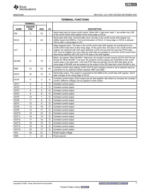
TERMINAL<br />
TERMINAL FUNCTIONS<br />
DBQ/PW/<br />
NAME PWP RGE I/O DESCRIPTION<br />
SIN 2 23 I<br />
Serial data input for driver on/off control. When SIN = high level, data '1' are written into LSB<br />
of the on/off control shift register at the rising edge of SCLK.<br />
Serial data shift clock. Schmitt buffer input. All data in the on/off control shift register are<br />
SCLK 3 24 I shifted toward the MSB by 1-bit synchronization of SCLK. A rising edge on SCLK is allowed<br />
100 ns after a rising edge of LAT.<br />
Edge triggered latch. The data in the on/off control data shift register are transferred to the<br />
on/off control data latch at this rising edge. At the same time, the data in the on/off control shift<br />
LAT 4 1 I register are replaced <strong>with</strong> <strong>LED</strong> open detection (LOD) and pre-thermal warning (PTW) data.<br />
LAT must be toggled only once after the shift data are updated to avoid the on/off control latch<br />
data being replaced <strong>with</strong> LOD and PTW data in the shift register.<br />
BLANK 21 18 I<br />
Blank, all outputs. When BLANK = high level, all constant current outputs (OUT0–OUT15) are<br />
forced off. When BLANK = low level, all constant current outputs are controlled by the on/off<br />
control data in the data latch. LOD and PTW data are latched into the SID data latch at the<br />
rising edge of BLANK and are present at the output of the SID data latch when BLANK is low.<br />
<strong>Constant</strong> current value setting, OUT0–OUT15 sink constant current is set to desired value by<br />
IREF 23 20 I/O connection to an external resistor between IREF and GND.<br />
SOUT 22 19 O<br />
OUT0 5 2 O<br />
OUT1 6 3 O <strong>Constant</strong> current output<br />
OUT2 7 4 O <strong>Constant</strong> current output<br />
OUT3 8 5 O <strong>Constant</strong> current output<br />
OUT4 9 6 O <strong>Constant</strong> current output<br />
OUT5 10 7 O <strong>Constant</strong> current output<br />
OUT6 11 8 O <strong>Constant</strong> current output<br />
OUT7 12 9 O <strong>Constant</strong> current output<br />
OUT8 13 10 O <strong>Constant</strong> current output<br />
OUT9 14 11 O <strong>Constant</strong> current output<br />
OUT10 15 12 O <strong>Constant</strong> current output<br />
OUT11 <strong>16</strong> 13 O <strong>Constant</strong> current output<br />
OUT12 17 14 O <strong>Constant</strong> current output<br />
OUT13 18 15 O <strong>Constant</strong> current output<br />
OUT14 19 <strong>16</strong> O <strong>Constant</strong> current output<br />
OUT15 20 17 O <strong>Constant</strong> current output<br />
VCC 24 21 — Power-supply voltage<br />
GND 1 22 — Power ground<br />
Serial data output. This output is connected to the MSB of the on/off data shift register. SOUT<br />
data changes at the rising edge of SCLK.<br />
<strong>Constant</strong> current output. Each output can be tied together <strong>with</strong> others to increase the constant<br />
current. Different voltages can be applied to each output.<br />
Copyright © 2008, Texas Instruments Incorporated Submit Documentation Feedback 7<br />
Product Folder Link(s): TLC5928