

lumped, inductorless oscillators - Stanford Technology CAD Home ...
lumped, inductorless oscillators - Stanford Technology CAD Home ...
lumped, inductorless oscillators - Stanford Technology CAD Home ...

You also want an ePaper? Increase the reach of your titles
YUMPU automatically turns print PDFs into web optimized ePapers that Google loves.
LUMPED, INDUCTORLESS OSCILLATORS: HOW FAR CAN THEY GO?<br />
Abstract<br />
The fundamental question of how much we can ultimately<br />
reduce the phase noise of a <strong>lumped</strong>, <strong>inductorless</strong> oscillator<br />
through careful design is addressed and it is shown that the<br />
fluctuation dissipation theorem of thermodynamics imposes<br />
a lower limit on the phase noise. An analytical formulation<br />
of this limit is presented and it is shown that the phase noise<br />
of ring <strong>oscillators</strong> with long-channel MOS devices is closer<br />
to this limit compared to that of the relaxation <strong>oscillators</strong> or<br />
ring <strong>oscillators</strong> with short channel MOS devices.<br />
Introduction<br />
Due to the increasing demand for high-level integration of<br />
electronic circuits, <strong>lumped</strong>, <strong>inductorless</strong> <strong>oscillators</strong> (LIOs)<br />
have become an extremely attractive choice for today’s IC<br />
designers. Relaxation and ring <strong>oscillators</strong> are used in several<br />
applications including clock recovery circuits for serial data<br />
communications (1) and on-chip clock distribution (2).<br />
However, applications in radio frequency (RF) circuits is<br />
quite limited mainly due to inferior phase noise behavior<br />
compared to inductor-based <strong>oscillators</strong>. Although several<br />
investigations have been performed to improve the phasenoise<br />
of LIOs (e.g. (3)), the fundamental question of whether<br />
or not there is a minimum achievable phase noise for this<br />
class of <strong>oscillators</strong> has not been addressed. This lingering<br />
question causes a great deal of uncertainty about the scalability<br />
of RFIC design without using tuned circuits.<br />
In this paper we address this question and show that one<br />
of the fundamental principles of thermodynamics sets a<br />
lower limit on the phase noise of LIOs. Using a simplified<br />
model, we then present a quantitative analysis of this minimum<br />
achievable phase noise. Finally, we present several<br />
examples from previously published results on relaxation<br />
and ring <strong>oscillators</strong> to compare the minimum achievable<br />
phase noise to the experimental results from real designs.<br />
Reza Navid, Thomas H. Lee, and Robert W. Dutton<br />
Center for Integrated Systems, <strong>Stanford</strong> University<br />
420 Via Palou, <strong>Stanford</strong>, CA 94305-4070 USA<br />
The Physical Argument for Minimum Achievable Phase<br />
Noise<br />
The phase noise of an oscillator is an indication of the fact<br />
that the oscillator is not continuously oscillating with the<br />
same frequency. To build a stable (and hence low-phasenoise)<br />
oscillator, one should be able to enforce the period of<br />
oscillation in a reliable fashion. In other words, a constant<br />
with the dimension of time is required to dictate the oscillation<br />
period. In inductor-based <strong>oscillators</strong> (like the Colpitts)<br />
this constant is LC were L is the inductor and C is the<br />
capacitor. In transmission-line-based <strong>oscillators</strong> the ratio of<br />
l ⁄ v establishes the time constant in which l is the length of<br />
the transmission line and v is the velocity of electromagnetic<br />
wave inside the transmission line. In LIOs the product of RC<br />
is usually the time constant. There is, however, a fundamental<br />
difference between this latter case and the first two ones.<br />
The fluctuation dissipation theorem of thermodynamics dictates<br />
that there exists a finite amount of thermal noise associated<br />
with any resistor. Thus, in contrast to inductor-based<br />
and transmission-line-based <strong>oscillators</strong>, the time constant of<br />
LIOs is inherently noisy because of the resistor noise. Consequently,<br />
even if the rest of the circuit is noise-free, the<br />
resistor noise imposes a lower limit on the phase noise of<br />
LIOs.<br />
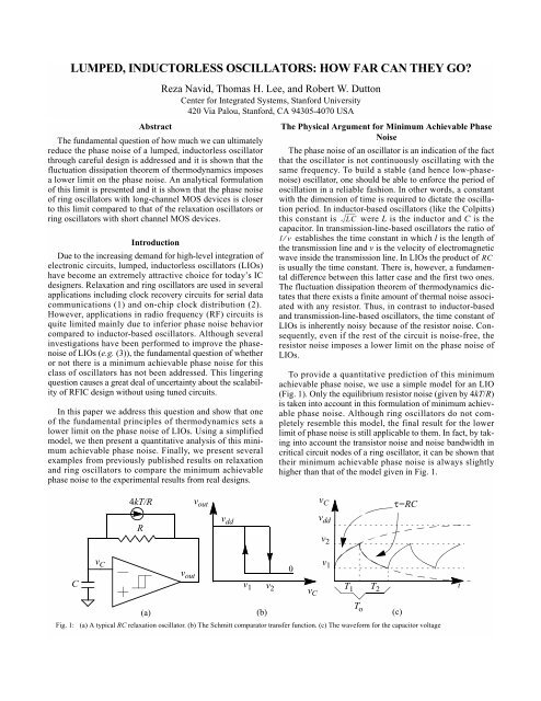
To provide a quantitative prediction of this minimum<br />
achievable phase noise, we use a simple model for an LIO<br />
(Fig. 1). Only the equilibrium resistor noise (given by 4kT/R)<br />
is taken into account in this formulation of minimum achievable<br />
phase noise. Although ring <strong>oscillators</strong> do not completely<br />
resemble this model, the final result for the lower<br />
limit of phase noise is still applicable to them. In fact, by taking<br />
into account the transistor noise and noise bandwidth in<br />
critical circuit nodes of a ring oscillator, it can be shown that<br />
their minimum achievable phase noise is always slightly<br />
higher than that of the model given in Fig. 1.<br />
Fig. 1:<br />
C<br />
4kT/R v out<br />
v C τ=RC<br />
v dd<br />
v dd<br />
R<br />
v 2<br />
v C v 1<br />
v<br />
0<br />
out<br />
v 1 v 2<br />
T 1 T 2<br />
T<br />
(a) (b) o (c)<br />
(a) A typical RC relaxation oscillator. (b) The Schmitt comparator transfer function. (c) The waveform for the capacitor voltage<br />
v C<br />
t
Analytical Formulation of Phase Noise for the RC<br />
Relaxation Oscillator<br />
Fig. 1 shows a typical RC relaxation oscillator, which will<br />
be used as a simplified model for an LIO. The oscillator is<br />
composed of a Schmitt comparator in an RC feedback loop.<br />
We first derive the basic equations governing the behavior of<br />
this oscillator and present an analysis of the jitter. In this analysis,<br />
the equilibrium resistor noise (given by 4kT/R) is taken<br />
into account while all other noise sources associated with the<br />
comparator and all non-equilibrium noise sources (like 1/f<br />
noise) are neglected. We then provide an analytical formulation<br />
of phase noise for this relaxation oscillator. The expression<br />
that we derive provides the minimum achievable phase<br />
noise dictated by the first principles of thermodynamics.<br />
C<br />
R<br />
–-------<br />
t<br />
RC<br />
e t<br />
v C<br />
() t = ----------- e<br />
C ∫0<br />
τ<br />
-------<br />
RC<br />
2 4kT∆f<br />
i n() f = ---------------<br />
R<br />
i n<br />
( τ)i n<br />
( τ' )<br />
2<br />
∆v C ( 0)<br />
= 0<br />
i n<br />
( τ) dτ<br />
2kTδ( τ–<br />
τ' )<br />
= -----------------------------<br />
R<br />
Fig. 2: The circuit model and the basic equations for calculating the variance<br />
of the capacitor voltage at any time t (v C (t)) given that its value is<br />
accurately known at time t=0.<br />
(5)<br />
i n<br />
t ∞<br />
A. Frequency and Minimum Power Dissipation<br />
The oscillator of Fig. 1 works as follows: during the first<br />
half of the period, the capacitor voltage changes exponentially<br />
from v 1 to v 2 (the two comparison levels). The duration of the<br />
first half of the period is found to be<br />
T 1<br />
v dd<br />
– v 1<br />
= RC × ln ------------------<br />
⎝<br />
⎛ v dd<br />
– v 2<br />
⎠<br />
⎞<br />
(1)<br />
Since i n is a Gaussian process with zero mean, (5) dictates<br />
that v C is also a Gaussian process with zero mean. Consequently,<br />
the fluctuations of v C will be completely described by<br />
finding its variance. Using (5) we can find the variance of v C :<br />
v C<br />
2<br />
2t<br />
–-------<br />
RC<br />
e t t<br />
() t = ----------- e<br />
C 2<br />
∫0∫<br />
τ + τ'<br />
-----------<br />
RC<br />
0<br />
i n<br />
( τ)i n<br />
τ'<br />
( ) dτdτ'<br />
(6)<br />
Similarly, the duration of the second half of the period is<br />
T 2<br />
v 2<br />
= RC × ln ----<br />
⎝<br />
⎛ ⎠<br />
⎞<br />
v 1<br />
(2)<br />
in which i n<br />
( τ)i n<br />
( τ' ) is the autocorrelation function of the noise<br />
source whose value is given in the onset of Fig. 2. Using this<br />
autocorrelation function in (6) and performing the integration,<br />
and the frequency of oscillation is given by<br />
f<br />
1<br />
osc<br />
= ----- = -----------------<br />
1<br />
=<br />
T o<br />
T 1<br />
+ T 2<br />
where T o is the period of oscillation.<br />
-------------------------------------------------------<br />
1<br />
v dd<br />
– v 1<br />
v<br />
RC ------------------ 2<br />
× ln × ----<br />
⎝<br />
⎛ v dd<br />
– v 2<br />
v 1<br />
⎠<br />
⎞<br />
(3)<br />
The absolute minimum power dissipation of this oscillator<br />
(neglecting the power consumed by the comparator) is dictated<br />
by the amount of charge transferred to the capacitor as<br />
its voltage moves between v 1 and v 2 in each cycle:<br />
P min<br />
= v dd<br />
Cv ( 2<br />
– v 1<br />
)f osc<br />
(4)<br />
B. Jitter<br />
The jitter is generated by the fluctuations of v C which are in<br />
turn caused by the resistor noise. The probability density function<br />
of the fluctuations of v C at any given time t can be found<br />
using the circuit model of Fig. 2. Assuming that the capacitor<br />
voltage is zero at t=0, this voltage as a function of the noise<br />
current, i n , is given by<br />
the variance of v C is found to be 1 2t<br />
2 kT⎛<br />
–-------<br />
RC⎞<br />
v C() t = ----- ⎜1 – e ⎟<br />
(7)<br />
C ⎝ ⎠<br />
Note that as → the variance of v C converges to kT/C<br />
and becomes independent of R. By replacing t in (7) by T 1 or<br />
T 2 , we can find the variance of the v C at the end of the first<br />
and second half-periods, respectively.<br />
As the capacitor voltage approaches the decision levels, the<br />
fluctuations of v C shifts the switching instance form its anticipated<br />
time and hence results in jitter. As far as the timing jitter<br />
for T 1 (T 2 ) is concerned, the fluctuations of v C can be interpreted<br />
as some uncertainty on the decision level v 2 (v 1 ). Using<br />
(1) and (2) the variances of T 1 and T 2 are then evaluated as:<br />
∂T 1<br />
2<br />
( ∆T 1<br />
) 2 = ( ∆v 2<br />
) 2 = ⎛------------------<br />
RC ⎞ 2 ( ∆v<br />
∂v ⎝v 2<br />
dd<br />
– v 2<br />
⎠ C<br />
) 2<br />
∂T 2<br />
2<br />
( ∆T 2<br />
) 2 = ( ∆v 1<br />
) 2 = ⎛ RC ------- ⎞ 2<br />
∂v ⎝ v 1<br />
1<br />
⎠<br />
( ∆v C<br />
) 2<br />
(8)<br />
(9)<br />
1. The presented derivation is simplified for brevity. A rigorous derivation<br />
shows that the final result is, nevertheless, correct.
where the linearization approximation is justified due to the<br />
fact that the noise level is always small. The total uncertainty<br />
in the period (cycle-to-cycle jitter) is given by:<br />
T o<br />
( ∆T o<br />
) 2 kTR 2 ⎛ 1 1 ⎞⎛<br />
–-------<br />
RC⎞<br />
= C⎜-------------------------<br />
+ ----<br />
⎝( v dd<br />
– v 2<br />
) 2 ⎟⎜<br />
1 – e ⎟<br />
2<br />
v ⎠⎝<br />
⎠<br />
1<br />
(10)<br />
We have assumed a duty cycle of 50% so that we can replace<br />
2t in (7) by T o . Note also that ∆T 1 and ∆T 2 are uncorrected<br />
variables. The switching takes place exactly when v C equals<br />
v 1 or v 2 . Consequently, at the beginning of each half cycle the<br />
value of v C is known accurately. Since the only noise source<br />
taken into account is white, the uncertainty of v C and hence<br />
T 1,2 at the end of each half cycle is completely independent of<br />
the one at the end of previous half cycle. This ensures us that<br />
∆T 1 and ∆T 2 are in fact independent.<br />
After solving (3) for R and using it in (10) we get<br />
( ∆T o<br />
) 2 kT<br />
( 1–<br />
2v<br />
------------------------<br />
1n<br />
)<br />
= ⋅ ---------------------------------------------------------------<br />
2 2<br />
2Cf osc<br />
v<br />
2 1<br />
dd v ln 1n<br />
------- – 1<br />
⎝<br />
⎛ ⎠<br />
⎞2 ( 1 – v1n ) 2<br />
(11)<br />
where v 1n<br />
= v 1<br />
⁄ v dd<br />
is the normalized decision level. We have<br />
assumed v 2 =v dd -v 1 , which ensures a duty cycle of 50%. The<br />
second part of (11), called the normalized jitter, is only a function<br />
of v 1n and can be plotted versus this parameter. Fig. 3<br />
present such a plot showing that the normalized jitter is minimized<br />
for v 1n =0.24. For constant values of temperature,<br />
capacitance, oscillation frequency and bias voltage, jitter (and<br />
hence phase noise) assumes its minimum value for v 1 =0.24v dd<br />
and v 2 =0.76v dd . Hereafter, we will use these values to find the<br />
minimum achievable phase noise. The minimum power dissipation<br />
and minimum cycle-to-cycle jitter are then found to be<br />
P min<br />
=<br />
(12)<br />
(13)<br />
C. Phase Noise<br />
The output of the relaxation oscillator of Fig. 1 is a stochastic<br />
square wave signal with mutually-independent, Gaussiandistribution<br />
cycle-to-cycle jitter. As presented in (4), the phase<br />
noise of such a signal has a close-to-Lorentzian shape around<br />
each harmonic. The phase noise around the first harmonic at<br />
an offset frequency of ∆ω = ω – 2πf osc<br />
is given by<br />
v 1n<br />
2<br />
0.52Cf osc<br />
v dd<br />
( ∆T o<br />
) 2 = 2( ∆T 1<br />
) 2 = --------------------<br />
5.9kT =<br />
PN( ∆f)<br />
2 2<br />
Cf osc<br />
v dd<br />
--------------------<br />
3.1kT<br />
P min<br />
f osc<br />
3 2<br />
f 0( ∆T)<br />
= ---------------------------------------------------------<br />
3 2<br />
( πf 0 ( ∆T)<br />
) 2 + ( f–<br />
f 0<br />
) 2<br />
(14)<br />
Normalized jitter<br />
22<br />
20<br />
18<br />
16<br />
14<br />
12<br />
10<br />
This equation predicts that the phase noise has a 1/f 2 shape<br />
for sufficiently large offset frequencies, which is consistent<br />
with the previously reported measurement results ((5) and<br />
(6)). Using (13) in (14) the phase noise at these offset frequencies<br />
is found to be<br />
PN( ∆f)<br />
0.1 0.2 0.3 0.4<br />
v 1n<br />
Fig. 3: Normalized jitter vs normalized decision level v 1n .<br />
5.9f osc<br />
kT<br />
= ------------------------ =<br />
2<br />
( ∆f) 2<br />
Cv dd<br />
3.1kT<br />
------------- ⎛ f osc<br />
-------- ⎞ 2<br />
P min<br />
⎝ ∆f ⎠<br />
(15)<br />
The phase noise is inversely proportional to the minimum<br />
power dissipation, which is in turn proportional to the capacitor<br />
value and the square of the bias voltage.<br />
Experimental Results<br />
The expression given in (15) provides the minimum<br />
achievable phase-noise for the idealized version of the relaxation<br />
oscillator shown in Fig. 1. Most practical relaxation<br />
<strong>oscillators</strong>, however, are not implemented in this fashion.<br />
Fig. 4 provides the schematic and the design parameters of a<br />
CMOS relaxation oscillator reported in (5). Although this<br />
oscillator is not exactly of the same form as the idealized<br />
relaxation oscillator given in Fig. 1, it is still considered an<br />
LIO. In the case of the oscillator of Fig. 4, the charging and<br />
discharging mechanism of the capacitor is not through a resistor<br />
but rather through the current sources and the transistors.<br />
Nevertheless, these components are noisy and thus impose a<br />
minimum achievable phase noise for this architecture.<br />
Fig. 5 compares the phase noise reported in (5) to the minimum<br />
achievable phase noise given by the second part of (15)<br />
under a constraint of constant power. To calculate P min , we<br />
have assumed v dd =3.3V which is typical for the 0.5µm technology.<br />
The minimum achievable phase noise for this power<br />
level is -122.6dBc/Hz and -136.6dBc/Hz at 1MHz and 5MHz<br />
offset frequencies, respectively. The measured values reported<br />
in (5) are -102dBc/Hz and -115dBc/Hz. Without increasing<br />
the power dissipation, around 21dB of phase noise improvement<br />
is possible before hitting the limit line of minimum<br />
achievable phase noise dictated by the first principles of thermodynamics<br />
for this class of <strong>oscillators</strong>. A similar architecture<br />
is reported in (6) as a relaxation VCO, which draws<br />
2.3mA of current from a 6V power supply at 115MHz (Fig.<br />
5.a and Fig. 7 in (6)). Under constant power-constrained
R<br />
I B<br />
v dd<br />
C<br />
R<br />
W/L=100µ/0.5µ<br />
g m =1/84<br />
R=275Ω<br />
C=0.6pF<br />
I B =3mA<br />
f osc =920MHz<br />
Fig. 4: The schematic and design parameters of the relaxation oscillator<br />
reported in (5).<br />
design, (15) predicts that the minimum achievable phase noise<br />
for this oscillator is -139dBc/Hz at an offset frequency of<br />
1MHz. This is again 21dB lower than the reported value of -<br />
118dBc/Hz given in (6). These two examples illustrate that the<br />
relaxation oscillator configuration is not an optimum choice in<br />
terms of the power-phase noise tradeoff.<br />
Experimental data on ring <strong>oscillators</strong> shows that these<br />
<strong>oscillators</strong> perform better in terms of power-phase noise<br />
tradeoff. Table I compares the measurement results reported in<br />
(3) to the theoretical prediction of the minimum achievable<br />
phase noise for the same power. The index numbers are the<br />
same as the ones assigned in (3). N is the number of stages<br />
and L min is the channel length of the smallest transistor in the<br />
circuit. The data is presented in descending order of L min . The<br />
difference between measured and predicted phase noise in this<br />
case is smaller than 9dB with most numbers around 6dB much<br />
better than the relaxation oscillator case. The difference<br />
between the minimum achievable phase noise and the measured<br />
phase noise increases with decreasing L min . This can<br />
possibly be attributed to the excess noise in short-channel<br />
MOS devices the origins of which is discussed in (7).<br />
Conclusion<br />
The lower limit of phase noise in LIOs is shown to be dictated<br />
by the fluctuation dissipation theorem of thermodynamics.<br />
Using a simplified model for this class of <strong>oscillators</strong>, a<br />
quantitative prediction of this minimum achievable phase<br />
noise is presented and the phase noise is expressed as a function<br />
of temperature, power dissipation, frequency of oscillation<br />
and the offset frequency. The phase noise of ring<br />
<strong>oscillators</strong> is generally closer to this limit compared to that of<br />
the relaxation <strong>oscillators</strong>, making a ring oscillator a more<br />
attractive choice in terms of power-phase noise tradeoff. It is<br />
shown that the phase noise improvement through careful<br />
design is fundamentally limited to 5 to 10dB for practical ring<br />
oscillator designs. The difference between the minimum<br />
achievable phase noise and the actual measured phase noise of<br />
a typical ring <strong>oscillators</strong> increases as we shrink the channel<br />
length of the MOS devices, which can be explained as due to<br />
the excess noise in short-channel MOS devices.<br />
I B<br />
Ω<br />
Phase Noise (dBc)<br />
0<br />
-20<br />
-40<br />
-60<br />
-80<br />
-100<br />
20.6dB<br />
21.6dB<br />
-120<br />
-140<br />
-5.E+06 -3.E+06 -1.E+06 1.E+06 3.E+06 5.E+06<br />
Offset Frequency (Hz)<br />
Fig. 5: Minimum achievable phase noise compared to the data reported in<br />
(5) for an oscillator with f osc =920MHz and P min =19.8mW at T=300 o K.<br />
Table I: Experimental results vs. theoretical prediction of minimum<br />
achievable phase noise at ∆f=1MHz for the ring <strong>oscillators</strong> of (3).<br />
Index<br />
N<br />
L min<br />
µm<br />
f osc<br />
MHz<br />
Power<br />
mW<br />
PN meas.<br />
dBc/Hz<br />
PN min<br />
dBc/Hz<br />
∆PN<br />
dB<br />
Current<br />
Starved<br />
1 5 2 232 1.5 -118.5 -123.4 4.6 No<br />
2 11 2 115 2.5 -126 -131.7 5.7 No<br />
4 3 0.53 751 5.85 -114 -119.1 5.1 Yes<br />
5 5 0.39 850 6.27 -112.6 -118.3 5.7 Yes<br />
6 7 0.36 931 6.22 -111.7 -117.5 5.8 Yes<br />
7 9 0.32 932 6.82 -112.5 117.9 5.4 Yes<br />
8 11 0.32 869 6.62 -112.2 118.3 6.1 Yes<br />
9 15 0.28 929 7 -112.3 118 5.7 Yes<br />
10 17 0.25 898 9.5 -112 119.6 7.6 Yes<br />
11 19 0.25 959 9.75 -110.9 119.2 8.3 Yes<br />
3 19 0.25 1330 25 -111.5 120.4 8.9 No<br />
Acknowledgments<br />
This work is supported under an SRC customized research<br />
project from Texas Instrument and MARCO MSD center.<br />
References<br />
(1) L. DeVito, J. Newton, R. Croughwell, J. Bulzacchelli, and F. Benkley,<br />
“A 52MHz and 155MHz clock-recovery PLL,” in ISSCC Dig.<br />
Tech. Papers, Feb. 1991, pp.142-143.<br />
(2) I. A. Young, J. K. Greason, and K. L. Wong, “A PLL clock generator<br />
with 5 to 110MHz of lock range for microprocessors,” IEEE J.<br />
Solid-State Circuits, vol. 27, pp. 1599-1607, Nov. 1992.<br />
(3) A. Hajimiri, S. Limotyrakis, and T. H. Lee, “Jitter and phase noise<br />
in ring <strong>oscillators</strong>,” IEEE J. Solid-State Circuits, vol. 34, pp. 790-804,<br />
June 1999.<br />
(4) R. Navid, T. H. Lee, and R. W. Dutton, “An analytical formulation<br />
of phase noise of signals with Gaussian distribution jitter,” unpublished.<br />
(5) B. Razavi, “A study of phase noise in CMOS <strong>oscillators</strong>,” IEEE J.<br />
Solid-State Circuits, vol. 31, pp. 331-343, Mar. 1996.<br />
(6) J. G. Sneep and C. J. M. Verhoeven, “A new low-noise 100-MHz<br />
balanced relaxation oscillator,” IEEE J. Solid-State Circuits, vol. 25,<br />
pp. 692-698, Jun. 1990.<br />
(7) R. Navid and R. W. Dutton, “The physical phenomena responsible<br />
for excess noise in short-channel MOS devices,” in International Conference<br />
on Simulation of Semiconductor Processes and Devices (SIS-<br />
PAD) Dig. Tech. Papers, Sep. 2002, pp. 75-78.


