IUP GEII - Abcelectronique
IUP GEII - Abcelectronique
IUP GEII - Abcelectronique

You also want an ePaper? Increase the reach of your titles
YUMPU automatically turns print PDFs into web optimized ePapers that Google loves.
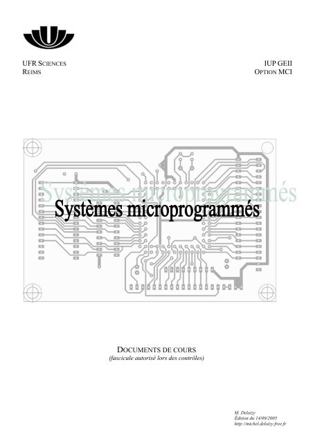
UFR SCIENCES<br />
REIMS<br />
<strong>IUP</strong> <strong>GEII</strong><br />
OPTION MCI<br />
DOCUMENTS DE COURS<br />
(fascicule autorisé lors des contrôles)<br />
M. Deloizy<br />
Édition du 14/09/2005<br />
http://michel.deloizy.free.fr
Chronogrammes du 6809 (Motorola)<br />
6809 - 2 -
Circuits périphériques - 3 -<br />
UVPROM Am27C64 (8k x 8)
HN58S65AI (EEPROM)<br />
Circuits périphériques - 4 -
HM65764 (RAM statique)<br />
Circuits périphériques - 5 -
TL16C450 (Communication série)<br />
Brochage, Chronogrammes<br />
Circuits périphériques - 6 -<br />
Description des signaux<br />
A0<br />
A1<br />
A2<br />
I<br />
Register select. A0, A1, and A2 are three inputs used during read and write operations to select the<br />
ACE register to read from or write to. Refer to Table 1 for register addresses, also refer to the<br />
address strobe ( ADS ) signal description.<br />
ADS I Address strobe. When ADS is active (low), the register select signals (A0, A1, and A2) and chip<br />
select signals (CS0, CS1, CS 2 ) drive the internal select logic directly; when high, the register select<br />
and chip select signals are held in the state they were in when the low-to-high transition of ADS<br />
occurred.<br />
BAUDOUT O Baud out. BAUDOUT is a16× clock signal for the transmitter section of the ACE. The clock rate is<br />
established by the reference oscillator frequency divided by a divisor specified by the baud generator<br />
divisor latches.<br />
BAUDOUT may also be used for the receiver section by tying this output to the RCLK input.<br />
CS0, CS1,<br />
CS 2<br />
I Chip select. When CSx is active (high, high, and low respectively), the ACE is selected. Refer to the<br />
ADS signal description.
Circuits périphériques - 7 -<br />
CSOUT O Chip select out. When CSOUT is high, it indicates that the ACE has been selected by the chip select<br />
inputs (CS0, CS1, and CS 2 ). CSOUT is low when the chip is deselected.<br />
CTS I Clear to send. CTS is a modem status signal. Its condition can be checked by reading bit 4 (CTS) of<br />
the modem status register. Bit 0 (DCTS) of the modem status register indicates that this signal has<br />
changed states since the last read from the modem status register. If the modem status interrupt is<br />
enabled when CTS changes state, an interrupt is generated.<br />
D0 – D7 I/O Data bus. D0 – D7 are 3-state data lines that provide a bidirectional path for data, control, and status<br />
information between the ACE and the CPU.<br />
DCD I Data carrier detect. DCD is a modem status signal. Its condition can be checked by reading bit 7<br />
(DCD) of the modem status register. Bit 3 (DDCD) of the modem status register indicates that this<br />
signal has changed states since the last read from the modem status register. If the modem status<br />
interrupt is enabled when the DCD changes state, an interrupt is generated.<br />
DDIS O Driver disable. DDIS is active (high) when the CPU is not reading data. When active, this output can<br />
disable an external transceiver.<br />
DISTR<br />
DIS TR<br />
I Data input strobes. When either DISTR or DIS TR is active (high or low respectively) while the ACE<br />
is selected, the CPU is allowed to read status information or data from a selected ACE register. Only<br />
one of these inputs is required for the transfer of data during a read operation. The other input should<br />
be tied in its inactive state (i.e., DISTR tied low or DIS TR tied high).<br />
DOSTR<br />
DOS TR<br />
I Data output strobes. When either DOSTR or DOS TR is active (high or low respectively), while the<br />
ACE is selected, the CPU is allowed to write control words or data into a selected ACE register.<br />
Only one of these inputs is required to transfer data during a write operation. The other input should<br />
be tied in its inactive state (i.e., DOSTR tied low or DOS TR tied high).<br />
DSR I Data set ready. DSR is a modem status signal. Its condition can be checked by reading bit 5 (DSR)<br />
of the modem status register. Bit 1 (DDSR) of the modem status register indicates that this signal<br />
has changed state since the last read from the modem status register. If the modem status interrupt is<br />
enabled when the DSR changes state, an interrupt is generated.<br />
D TR O Data terminal ready. When active (low), D TR informs a modem or data set that the ACE is ready to<br />
establish communication. DTR<br />
is placed in the active state by setting the DTR bit of the modem<br />
control register to a high level. D TR is placed in the inactive state either as a result of a master reset<br />
or during loop mode operation or clearing bit 0 (DTR) of the modem control register.<br />
INTRPT O Interrupt. When active (high), INTRPT informs the CPU that the ACE has an interrupt to be<br />
serviced. The four conditions that cause an interrupt are: a receiver error, received data is available,<br />
the transmitter holding register is empty, or an enabled modem status interrupt. The INTRPT output<br />
is reset (inactivated) either when the interrupt is serviced or as a result of a master reset.<br />
MR I Master reset. When active (high), MR clears most ACE registers and sets the state of various output<br />
signals.<br />
Refer to Table 2 for ACE reset functions.<br />
OUT 1<br />
OUT 2<br />
O Outputs 1 and 2. OUT 1 and OUT2<br />
are user-designated output terminals that are set to their active<br />
states by setting their respective modem control register bits (OUT1 and OUT2) high. OUT 1 and<br />
OUT 2 are set to their inactive (high) states as a result of master reset or during loop mode operations<br />
or by clearing bit 2 (OUT1) or bit 3 (OUT2) of the MCR.<br />
RCLK I Receiver clock. RCLK is the 16 × baud rate clock for the receiver section of the ACE.<br />
RI I Ring indicator. RI is a modem status signal. Its condition can be checked by reading bit 6 (RI) of the<br />
modem status register. Bit 2 (TERI) of the modem status register indicates that the RI input has<br />
transitioned from a low to a high state since the last read from the modem status register. If the<br />
modem status interrupt is enabled when this transition occurs, an interrupt is generated.<br />
RTS O Request to send. When active, RTS informs the modem or data set that the ACE is ready to transmit<br />
data. RTS is set to its active state by setting the RTS modem control register bit and is set to its<br />
inactive (high) state either as a result of a master reset or during loop mode operations or by clearing<br />
bit 1 (RTS) of the MCR.<br />
SIN I Serial input. SIN is the serial data input from a connected communications device.<br />
SOUT O Serial output. SOUT is the composite serial data output to a connected communication device.<br />
SOUT is set to the marking (set) state as a result of MR.<br />
V CC<br />
5-V supply voltage<br />
V SS<br />
Supply common<br />
XTAL1<br />
XTAL2<br />
I/O External clock. XTAL1 and XTAL2 connect the ACE to the main timing reference (clock or<br />
crystal).
Circuits périphériques - 8 -<br />
Autres circuits logiques<br />
Décodeurs démultiplexeurs<br />
74138<br />
74139
74139<br />
Circuits périphériques - 9 -<br />
Buffers<br />
74244
74245<br />
Circuits périphériques - 10 -<br />
Latches<br />
74373
Circuits périphériques 11<br />
AD7918 (Analog Devices)<br />
Pin Mnemonic Description<br />
1 VREF Reference Input, 1.2 V to VDD.<br />
2 VIN Analog Input, 0 V to VREF.<br />
3 GND Analog and Digital Ground.<br />
4 CONVST#<br />
Convert Start. A low-to-high transition on this pin initiates a 1.5 µs pulse on an<br />
internally generated CONVST# signal. A high-to-low transition on this line initiates<br />
the conversion process if the internal CONVST# signal is low. Depending on the<br />
signal on this pin at the end of a conversion, the AD7819 automatically powers<br />
down.<br />
5 CS# Chip Select. This is a logic input. CS# is used in conjunction with RD# to enable<br />
outputs.<br />
6 RD# Read Pin. This is a logic input. When CS# is low and RD# goes low, the DB7–<br />
DB0 leave their high impedance state and data is driven onto the data bus.<br />
7 BUSY ADC Busy Signal. This is a logic output. This signal goes logic high during the<br />
conversion process.<br />
8– DB0–DB7 Data Bit 0 to 7. These outputs are three-state TTL-compatible.<br />
15<br />
16 VDD Positive power supply voltage, 2.7 V to 5.5 V.<br />
Parameter VDD= 5 V ± 10% Unit Conditions/Comments<br />
tPOWER-UP<br />
1.5 µs (max) Power-Up Time of AD7819 after Rising Edge of CONVST.<br />
t1 4.5 µs (max) Conversion Time.<br />
t2 30 ns (min) CONVST# Pulsewidth.<br />
t3 30 ns (max) CONVST# Falling Edge to BUSY Rising Edge Delay.<br />
t4 0 ns (min) CS# to RD# Setup Time.<br />
t5 0 ns (min) CS# Hold Time after RD# High.<br />
t6 10 ns (max) Data Access Time after RD# Low.<br />
t7 10 ns (max) Bus Relinquish Time after RD# High.<br />
t8 100 ns (min) Data Bus Relinquish to Falling Edge of CONVST# Delay.
C167CR - 12 -<br />
C167CR<br />
Cette partie contient une documentation réduite du C167CR (Infineon), du compilateur C (Tasking) et<br />
des systèmes matériels étudiés (TQ tech.).<br />
Les informations et les graphes sont tous issus et recopiés à partir des documents techniques originaux.<br />
Certaines parties sont traduites, d'autres sont restées intentionnellement dans leur langue d'origine<br />
(l'anglais), qu'il est nécessaire de maîtriser afin de pouvoir mettre en œuvre les technologies actuelles.<br />
M. Deloizy
Présentation C167CR - 13 -<br />
Présentation<br />
Famille C166<br />
Versions du C167<br />
→ SAK-C167CR-16RM
Présentation C167CR - 14 -<br />
Architecture interne<br />
High Performance 16-bit CPU with four stage Pipeline<br />
• 80/60 ns minimum instruction cycle time, with most instructions executed in 1 cycle<br />
• 400/300 ns multiplication (16-bit x 16-bit), 800/600 ns division (32-bit/16-bit)<br />
• Multiple high bandwidth internal data buses<br />
• Register based design with multiple variable register banks<br />
• Single cycle context switching support<br />
• 16 MBytes linear address space for code and data (Von Neumann architecture)<br />
• System stack cache support with automatic stack overflow/underflow detection<br />
Control Oriented Instruction Set with High Efficiency<br />
• Bit, byte, and word data types<br />
• Flexible and efficient addressing modes for high code density<br />
• Enhanced boolean bit manipulation with direct addressability of 6 Kbits for peripheral control and<br />
user defined flags<br />
• Hardware traps to identify exception conditions during runtime<br />
• High Level Language support for semaphore operations and efficient data access<br />
Integrated On-chip Memory<br />
• 2 KByte internal RAM for variables, register banks, system stack and code<br />
• 2 KByte on-chip high-speed XRAM for variables, user stack and code (not on all derivatives)<br />
• 128 KByte or 32 KByte on-chip ROM (not for ROMless devices)<br />
External Bus Interface<br />
• Multiplexed or demultiplexed bus configurations<br />
• Segmentation capability and chip select signal generation<br />
• 8-bit or 16-bit data bus<br />
• Bus cycle characteristics selectable for five programmable address areas
Présentation C167CR - 15 -<br />
16-Priority-Level Interrupt System<br />
• 56 interrupt nodes with separate interrupt vectors<br />
• 240/180 ns typical interrupt latency (400/300 ns maximum) in case of internal program execution<br />
• Fast external interrupts<br />
8-Channel Peripheral Event Controller (PEC)<br />
• Interrupt driven single cycle data transfer<br />
• Transfer count option (std. CPU interrupt after programmable number of PEC transfers)<br />
• Eliminates overhead of saving and restoring system state for interrupt requests<br />
Intelligent On-chip Peripheral Subsystems<br />
• 16-channel 10-bit A/D Converter with programmable conversion time (7.76 ms minimum), auto<br />
scan modes, channel injection mode<br />
• Two 16-channel Capture/Compare Units with 2 independent time bases each, very flexible PWM<br />
unit/event recording unit with different operating modes, includes four 16-bit timers/counters,<br />
maximum resolution fCPU/8<br />
• 4-channel PWM unit<br />
• Two Multifunctional General Purpose Timer Units<br />
GPT1: Three 16-bit timers/counters, maximum resolution fCPU/8<br />
GPT2: Two 16-bit timers/counters, maximum resolution fCPU/4<br />
• Asynchronous/Synchronous Serial Channels (USART) with baud rate generator, parity, framing,<br />
and overrun error detection<br />
• High Speed Synchronous Serial Channel programmable data length and shift direction<br />
• On-chip CAN Bus Module, Rev. 2.0B active (not on all derivatives)<br />
• Watchdog Timer with programmable time intervals<br />
• Bootstrap Loader for flexible system initialization<br />
111 IO Lines with Individual Bit Addressability<br />
• Tri-stated in input mode<br />
• Selectable input thresholds (not<br />
on all pins)<br />
• Push/pull or open drain output<br />
mode<br />
• Programmable port driver control<br />
(fast/reduced edge)<br />
Different Temperature Ranges<br />
• 0 to + 70 °C, – 40 to + 85 °C, –<br />
40 to + 125 °C<br />
Infineon CMOS Process<br />
• Low power CMOS technology<br />
including power saving Idle and<br />
Power Down modes.<br />
144-pin Plastic Metric Quad Flat<br />
Pack (MQFP) Package<br />
• P-MQFP, 28 x 28 mm body, 0.65<br />
mm (25.6 mil) lead spacing,<br />
surface mount technology
Organisation mémoire C167CR - 16 -<br />
Organisation mémoire<br />
Architecture Von Neumann<br />
Espace mémoire unique pour ROM interne, RAM interne, SFRs, périphériques internes et mémoire<br />
externe.<br />
16 M-octets adressables<br />
- 256 segments de 64 Ko chacun<br />
- chaque segment est divisé en 4 pages de 16 Ko<br />
Mémoire interne essentiellement située dans le segment 0.<br />
• 0000h … 7FFFh : ROM / Flash ou OTP interne.<br />
Peut être déplacé en 10000h … 1FFFFh pour permettre ROM externe en adresse<br />
basse.<br />
• F000h … FFFFh : RAM interne et SFRs<br />
Code exécutable dans toute zone mémoire (RAM ou ROM), sauf dans les SFRs.<br />
Octets situés en adresses paires ou impaires.<br />
Mots (16 bits) situés en adresse paire (MSB en adresse impaire).<br />
Longs mots (32 bits) rangés comme 2 mots consécutifs (LSB en adresse paire).<br />
Bits adressables pour certains SFRs, une partie de la RAM interne et registres à usage général.
Organisation mémoire C167CR - 17 -<br />
RAM interne et SFR<br />
2 Ko de IRAM, 256 octets de SFRs<br />
Mémoire XRAM<br />
2 Ko. Mémoire interne située en page 3.<br />
Accessible comme RAM externe (sans utiliser les bus externes).<br />
Peut être désactivée par bit XPEN de SYSCON.<br />
Pas de Wait-states<br />
Accessible de l'extérieur en DMA
Organisation mémoire C167CR - 18 -<br />
Registres à usage général<br />
(registres de travail)<br />
Blocs de 16 mots consécutifs en RAM interne.<br />
Registre CP (Context Pointer) indique l'adresse de base de la banque de registres active.<br />
Internal RAM Address Byte Registers Word Register<br />
+ 1EH – R15<br />
+ 1CH – R14<br />
+ 1AH – R13<br />
+ 18H – R12<br />
+ 16H – R11<br />
+ 14H – R10<br />
+ 12H – R9<br />
+ 10H – R8<br />
+ 0EH RH7 RL7 R7<br />
+ 0CH RH6 RL6 R6<br />
+ 0AH RH5 RL5 R5<br />
+ 08H RH4 RL4 R4<br />
+ 06H RH3 RL3 R3<br />
+ 04H RH2 RL2 R2<br />
+ 02H RH1 RL1 R1<br />
+ 00H RH0 RL0 R0<br />
→ Permet commutation de contexte rapide par modification de CP.<br />
Instruction SCXT (Switch Context) réalise la commutation de banques et une sauvegarde automatique du<br />
contexte précédent.<br />
Mémoire externe<br />
4 tailles de banques mémoires possibles :<br />
- 64 Ko. Mode non segmenté. A15…A0 sur P0 et P1<br />
- 256 Ko. Mode segmenté 2 bits. A17,A16 sur P4 ; A15…A0 sur P0 et P1<br />
- 1 Mo. Mode segmenté 4 bits. A19…A16 sur P4 ; A15…A0 sur P0 et P1<br />
- 16 Mo. Mode segmenté 8 bits. A22…A16 sur P4 ; A15…A0 sur P0 et P1<br />
4 types de bus différents :<br />
bus adresses données<br />
multiplexé 16 bits P0 P0 (par défaut après RESET)<br />
multiplexé 8 bits P0 P0:7…0<br />
démultiplexé 16 bits P1 P0<br />
Démultiplexé 8 bits P1 P0:7…0<br />
Le modèle de mémoire et le type de bus est sélectionné pendant le RESET en agissant sur EA# et P0.<br />
Les adressages de bits ne sont pas possibles en mémoire externe.
CPU C167CR - 19 -<br />
CPU<br />
(Central Processing Unit)<br />
Architecture<br />
- ALU 16 bits<br />
- Pipeline à 4 étages (parallélisme)<br />
- Accès aux périphériques externes par EBC (External Bus Controller). Le CPU peut<br />
continuer à fonctionner en attendant que EBC effectue un accès externe.<br />
- Périphériques internes utilisent un générateur d'horloge distinct.<br />
- Contrôleur d'interruption intégré avec gestion des priorités.<br />
- Traitement d'interruptions par PEC (Peripheral Event Controller)<br />
- Interruptions logicielles, NMI traitées comme iT ordinaires<br />
- Watchdog<br />
- Modes faible consommation<br />
États CPU particuliers :<br />
- Reset : force le CPU dans un état prédéfini<br />
- IDLE : horloge du CPU arrêtée ; horloges des périphériques actives<br />
- POWER-DOWN : Toutes horloges arrêtées. Entrées des périphériques ignorées.<br />
Sortie du mode IDLE : par interruption<br />
Sortie du mode POWER-DOWN : par RESET
CPU C167CR - 20 -<br />
Pipeline<br />
Instruction exécutée en 4 étapes → 4 étages du pipeline fonctionnant simultanément.<br />
1. Recherche de l'instruction<br />
2. Décodage de l'instruction, calcul des adressages, récupération des éventuels opérandes<br />
3. Exécution de l'instruction. Utilisation de l'ALU. Mise à jour de PSW.<br />
4. Écriture des résultats dans RAM interne ou externe.<br />
Fonctionnement parallèle :<br />
Cycle machine<br />
FETCH I 1 I 2 I 3 I 4 I 5 I 6<br />
DECODE I 1 I 2 I 3 I 4 I 5<br />
EXECUTE I 1 I 2 I 3 I 4<br />
WRITEBACK I 1 I 2 I 3<br />
→ Beaucoup d'instructions s'exécutent en 1 cycle machine.<br />
Problèmes liés au pipeline :<br />
4 instructions traitées simultanément ⇒ risque de mauvaise exécution dans certains cas.<br />
→ le C167 insère parfois une "instruction injectée" dans le deuxième étage du pipeline quand une<br />
instruction ne peut pas être traitée complètement en 1 cycle.<br />
Exemple du branchement conditionnel : une instruction injectée est utilisée pour déterminer l'instruction<br />
désignée par le branchement.<br />
Certains cas nécessitent l'attention du programmeur :<br />
• Modification du contexte (changement de banque de registres)<br />
SCXT CP,#0FC00h ;sélection d'un nouveau contexte<br />
…<br />
;ne doit pas utiliser un registre (car ancien contexte encore actif)<br />
MOV R0,#data ;écrit data dans registre R0 du nouveau contexte<br />
• Modification du pointeur de page de données<br />
MOV DPP0,#4 ;sélection de la page de donnée 4<br />
…<br />
;ne doit pas utiliser une instruction utilisant DPP0<br />
MOV DPP0:0000H,R1 ;écrit R1 à l'adresse 10000H<br />
• Modification de la pile système<br />
MOV SP,#0FA40H ;définit un nouveau sommet de pile système<br />
…<br />
;ne doit pas utiliser d'instruction type POP,RET,…<br />
;PUSH,CALL,SCXT autorisés car résolus en interne<br />
POP R0<br />
;dépile R0 à partir de la nouvelle pile<br />
• Contrôle des interruptions<br />
IEN ou ILVL de PSW non pris en compte instantanément :<br />
BCLR IEN<br />
;désactive interruptions<br />
…<br />
;instruction encore interruptible<br />
…<br />
;interruptions désactivées (début d'une séquence critique)<br />
…<br />
BSET IEN<br />
;autorise interruptions (fin de la séquence critique)<br />
ou :<br />
ATOMIC #3<br />
;désactive immédiatement les interruptions<br />
BCLR IEN<br />
;interdit les interruptions<br />
…<br />
;séquence critique<br />
BSET IEN
CPU C167CR - 21 -<br />
• Initialisation des ports<br />
incorrect :<br />
BSET DP3.12 ;met le bit 12 de P3 en sortie<br />
BSET P3.9 ;P3.12 est encore une entrée ; rd/mod/wr lit P3.12<br />
correct :<br />
BSET DP3.12<br />
NOP<br />
BSET P3.9 ;P3.12 est en sortie ; rd/mod/wr lit le latch de la sortie P3.12<br />
Opérations sur bits<br />
Utilisent des cycles Lecture/Modification/Écriture sur octets.<br />
Actives uniquement sur les zone adressables par bits (RAM interne, SFRs).<br />
Pile système<br />
‣ utilisation des sous programmes<br />
‣ gestion des interruptions<br />
‣ sauvegardes gérées par le CPU<br />
• Pile de type LIFO<br />
• Utilise le registre SP (Stack Pointer)<br />
• SP évolue vers les adresses basses quand une donnée est rangée dans la pile.<br />
• Seules les données 16 bits sont autorisées.<br />
• STKOV et STKUN sont des registres qui permettent de contrôler les dépassements de pile.<br />
Ils permettent également la gestion d'une pile circulaire.
SFRs C167CR - 22 -<br />
SFRs (Special Function Registers)<br />
XPER-SHARE<br />
VISIBLE<br />
XPEN<br />
BDRSTEN<br />
OWDDIS<br />
CSCFG<br />
WRCFG<br />
CLKEN<br />
BYTDIS<br />
ROMEN<br />
SGTDIS<br />
ROMS1<br />
STKSZ<br />
XBUS Peripheral Share Mode Control<br />
0: External accesses to XBUS peripherals are disabled<br />
1: XBUS peripherals are accessible via the external bus during hold mode<br />
Visible Mode Control<br />
0: Accesses to XBUS peripherals are done internally<br />
1: XBUS peripheral accesses are made visible on the external pins<br />
XBUS Peripheral Enable Bit<br />
0: Accesses to the on-chip X-Peripherals and their functions are disabled<br />
1: The on-chip X-Peripherals are enabled and can be accessed<br />
Bidirectional Reset Enable Bit<br />
0: Pin RSTIN is an input only.<br />
1: Pin RSTIN is pulled low during the internal reset sequence after any reset.<br />
Oscillator Watchdog Disable Bit (Cleared after reset)<br />
0: The on-chip oscillator watchdog is enabled and active.<br />
1: The on-chip oscillator watchdog is disabled and the CPU clock is always fed from the oscillator<br />
input.<br />
Chip Select Configuration Control (Cleared after reset)<br />
0: Latched CS mode. The CS signals are latched internally and driven to the (enabled) port pins<br />
synchronously.<br />
1: Unlatched CS mode. The CS signals are directly derived from the address and driven to the<br />
(enabled) port pins.<br />
Write Configuration Control (Set according to pin P0H.0 during reset)<br />
0: Pins WR and BHE retain their normal function<br />
1: Pin WR acts as WRL, pin BHE acts as WRH<br />
System Clock Output Enable (CLKOUT, cleared after reset)<br />
0: CLKOUT disabled: pin may be used for general purpose IO<br />
1: CLKOUT enabled: pin outputs the system clock signal<br />
Disable/Enable Control for Pin BHE (Set according to data bus width)<br />
0: Pin BHE enabled<br />
1: Pin BHE disabled, pin may be used for general purpose IO<br />
Internal ROM Enable (Set according to pin EA during reset)<br />
0: Internal program memory disabled, accesses to the ROM area use the external bus<br />
1: Internal program memory enabled<br />
Segmentation Disable/Enable Control (Cleared after reset)<br />
0: Segmentation enabled (CSP is saved/restored during interrupt entry/exit)<br />
1: Segmentation disabled (Only IP is saved/restored)<br />
Internal ROM Mapping<br />
0: Internal ROM area mapped to segment 0 (00’0000H … 00’7FFFH)<br />
1: Internal ROM area mapped to segment 1 (01’0000H … 01’7FFFH)<br />
System Stack Size<br />
Selects the size of the system stack (in the internal RAM) from 32 to 512 words<br />
Stack Size (words) Internal RAM Addresses (words)<br />
0 0 0 256 00’FBFE … 00’FA00 (Default after Reset)<br />
0 0 1 128 00’FBFE … 00’FB00<br />
0 1 0 64 00’FBFE … 00’FB80<br />
0 1 1 32 00’FBFEH … 00’FBC0H<br />
1 0 0 512 00’FBFEH … 00’F800H<br />
1 0 1 – Reserved. Do not use this combination.<br />
1 1 0 – Reserved. Do not use this combination.<br />
1 1 1 1024 00’FDFEH … 00’F600H (Note: No circular stack)
SFRs C167CR - 23 -<br />
N<br />
C<br />
V<br />
Z<br />
E<br />
MULIP<br />
USR0<br />
HLDEN,<br />
ILVL,<br />
IEN<br />
Negative Result<br />
Set, when the result of an ALU operation is negative.<br />
Carry Flag<br />
Set, when the result of an ALU operation produces a carry bit.<br />
Overflow Result<br />
Set, when the result of an ALU operation produces an overflow.<br />
Zero Flag<br />
Set, when the result of an ALU operation is zero.<br />
End of Table Flag<br />
Set, when the source operand of an instruction is 8000H or 80H.<br />
Multiplication/Division In Progress<br />
0: There is no multiplication/division in progress<br />
1: A multiplication/division has been interrupted<br />
User General Purpose Flag May be used by the application software.<br />
Interrupt and EBC Control Fields<br />
Define the response to interrupt requests and enable external bus arbitration.<br />
En mode non segmenté, CSP est ignoré.
SFRs C167CR - 24 -<br />
Pointeurs de pages de données (DDPx)<br />
→ Sélection simultanée de 4 pages de données de 16 Ko dans l'ensemble de la mémoire.
SFRs C167CR - 25 -<br />
Pointeur de contexte (CP)<br />
→ Indique l'adresse de base du bloc de registres (GPR : General Purpose Registers) en RAM interne.<br />
Pointeur de Pile (SP)<br />
Poids fort Multiplication/Division (MDH)<br />
- 16x16→32 : 16 bits poids fort du résultat<br />
- 32:16→16+reste(16) : MDH contient 16 bits poids fort du dividende. Après la division,<br />
MDH contient le reste.<br />
Quand interruption, MDH doit être sauvegardé.
SFRs C167CR - 26 -<br />
Poids faible Multiplication/Division (MDL)<br />
Contrôle des multiplications/divisions<br />
MDRIU Multiply/Divide Register In Use<br />
0 : Cleared when register MDL is read via software<br />
1 : Set when register MDL or MDH is set via software, or when a multiply or divide<br />
instruction is executed.<br />
!! Internal Machine Status<br />
The multiply/divide unit uses these bits to control internal operations. Never modify these bits<br />
without saving and restoring register MDC<br />
Zéros et Uns
Interruptions C167CR - 27 -<br />
Interruptions<br />
‣ 56 sources d'interruption<br />
‣ 16 niveaux de priorité<br />
Quand une interruption est demandée :<br />
• l'exécution du programme est suspendue<br />
• l'état du programme courant est sauvegardé : IP, PSW et CSP (en mode segmenté) empilés<br />
• l'interruption la plus prioritaire est prise en compte<br />
• la routine d'interruption est exécutée<br />
• quand l'instruction RETI est trouvée, le contexte initial (IP, PSW et CSP) est récupéré et<br />
l'exécution du programme peut continuer.<br />
Une interruption sera prise en compte par le CPU si :<br />
- le flag IEN de PSW est à 1<br />
- le niveau de priorité de l'interruption demandée est supérieur à celui du CPU (indiqué dans<br />
PSW).<br />
Sources et vecteurs d'interruption<br />
Source of Interrupt or<br />
PEC Service Request<br />
Request<br />
Flag<br />
Enable<br />
Flag<br />
Interrupt<br />
Vector<br />
Vector<br />
Location<br />
Trap<br />
Number<br />
CAPCOM Register 0 CC0IR CC0IE CC0INT 00’0040H 10H/16D<br />
CAPCOM Register 1 CC1IR CC1IE CC1INT 00’0044H 11H/17D<br />
CAPCOM Register 2 CC2IR CC2IE CC2INT 00’0048H 12H/18D<br />
CAPCOM Register 3 CC3IR CC3IE CC3INT 00’004CH 13H/19D<br />
CAPCOM Register 4 CC4IR CC4IE CC4INT 00’0050H 14H/20D<br />
CAPCOM Register 5 CC5IR CC5IE CC5INT 00’0054H 15H/21D<br />
CAPCOM Register 6 CC6IR CC6IE CC6INT 00’0058H 16H/22D<br />
CAPCOM Register 7 CC7IR CC7IE CC7INT 00’005CH 17H/23D<br />
CAPCOM Register 8 CC8IR CC8IE CC8INT 00’0060H 18H/24D<br />
CAPCOM Register 9 CC9IR CC9IE CC9INT 00’0064H 19H/25D<br />
CAPCOM Register 10 CC10IR CC10IE CC10INT 00’0068H 1AH/26D<br />
CAPCOM Register 11 CC11IR CC11IE CC11INT 00’006CH 1BH/27D<br />
CAPCOM Register 12 CC12IR CC12IE CC12INT 00’0070H 1CH/28D<br />
CAPCOM Register 13 CC13IR CC13IE CC13INT 00’0074H 1DH/29D<br />
CAPCOM Register 14 CC14IR CC14IE CC14INT 00’0078H 1EH/30D<br />
CAPCOM Register 15 CC15IR CC15IE CC15INT 00’007CH 1FH/31D<br />
CAPCOM Register 16 CC16IR CC16IE CC16INT 00’00C0H 30H/48D<br />
CAPCOM Register 17 CC17IR CC17IE CC17INT 00’00C4H 31H/49D<br />
CAPCOM Register 18 CC18IR CC18IE CC18INT 00’00C8H 32H/50D<br />
CAPCOM Register 19 CC19IR CC19IE CC19INT 00’00CCH 33H/51D<br />
CAPCOM Register 20 CC20IR CC20IE CC20INT 00’00D0H 34H/52D<br />
CAPCOM Register 21 CC21IR CC21IE CC21INT 00’00D4H 35H/53D<br />
CAPCOM Register 22 CC22IR CC22IE CC22INT 00’00D8H 36H/54D<br />
CAPCOM Register 23 CC23IR CC23IE CC23INT 00’00DCH 37H/55D<br />
CAPCOM Register 24 CC24IR CC24IE CC24INT 00’00E0H 38H/56D<br />
CAPCOM Register 25 CC25IR CC25IE CC25INT 00’00E4H 39H/57D<br />
CAPCOM Register 26 CC26IR CC26IE CC26INT 00’00E8H 3AH/58D<br />
CAPCOM Register 27 CC27IR CC27IE CC27INT 00’00ECH 3BH/59D<br />
CAPCOM Register 28 CC28IR CC28IE CC28INT 00’00F0H 3CH/60D<br />
CAPCOM Register 29 CC29IR CC29IE CC29INT 00’0110H 44H/68D
Interruptions C167CR - 28 -<br />
CAPCOM Register 30 CC30IR CC30IE CC30INT 00’0114H 45H/69D<br />
CAPCOM Register 31 CC31IR CC31IE CC31INT 00’0118H 46H/70D<br />
CAPCOM Timer 0 T0IR T0IE T0INT 00’0080H 20H/32D<br />
CAPCOM Timer 1 T1IR T1IE T1INT 00’0084H 21H/33D<br />
CAPCOM Timer 7 T7IR T7IE T7INT 00’00F4H 3DH/61D<br />
CAPCOM Timer 8 T8IR T8IE T8INT 00’00F8H 3EH/62D<br />
GPT1 Timer 2 T2IR T2IE T2INT 00’0088H 22H/34D<br />
GPT1 Timer 3 T3IR T3IE T3INT 00’008CH 23H/35D<br />
GPT1 Timer 4 T4IR T4IE T4INT 00’0090H 24H/36D<br />
GPT2 Timer 5 T5IR T5IE T5INT 00’0094H 25H/37D<br />
GPT2 Timer 6 T6IR T6IE T6INT 00’0098H 26H/38D<br />
GPT2 CAPREL Register CRIR CRIE CRINT 00’009CH 27H/39D<br />
A/D Conversion Complete ADCIR ADCIE ADCINT 00’00A0H 28H/40D<br />
A/D Overrun Error ADEIR ADEIE ADEINT 00’00A4H 29H/41D<br />
ASC0 Transmit S0TIR S0TIE S0TINT 00’00A8H 2AH/42D<br />
ASC0 Transmit Buffer S0TBIR S0TBIE S0TBINT 00’011CH 47H/71D<br />
ASC0 Receive S0RIR S0RIE S0RINT 00’00ACH 2BH/43D<br />
ASC0 Error S0EIR S0EIE S0EINT 00’00B0H 2CH/44D<br />
SSC Transmit SCTIR SCTIE SCTINT 00’00B4H 2DH/45D<br />
SSC Receive SCRIR SCRIE SCRINT 00’00B8H 2EH/46D<br />
SSC Error SCEIR SCEIE SCEINT 00’00BCH 2FH/47D<br />
PWM Channel 0 … 3 PWMIR PWMIE PWMINT 00’00FCH 3FH/63D<br />
CAN1 XP0IR XP0IE XP0INT 00’0100H 40H/64D<br />
Unassigned node XP1IR XP1IE XP1INT 00’0104H 41H/65D<br />
Unassigned node XP2IR XP2IE XP2INT 00’0108H 42H/66D<br />
PLL/OWD XP3IR XP3IE XP3INT 00’010CH 43H/67D<br />
Exception Condition Trap Flag Trap<br />
Vector<br />
Vector<br />
Location<br />
Trap<br />
Number<br />
Trap<br />
Prior.<br />
Reset Functions<br />
Hardware Reset RESET 00’0000H 00H III<br />
Software Reset RESET 00’0000H 00H III<br />
Watchdog Timer Overflow RESET 00’0000H 00H III<br />
Class A Hardware Traps<br />
Non-Maskable Interrupt NMI NMITRAP 00’0008H 02H II<br />
Stack Overflow STKOF STOTRAP 00’0010H 04H II<br />
Stack Underflow STKUF STUTRAP 00’0018H 06H II<br />
Class B Hardware Traps<br />
Undefined Opcode UNDOPC BTRAP 00’0028H 0AH I<br />
Protected Instruction Fault PRTFLT BTRAP 00’0028H 0AH I<br />
Illegal Word Operand Access ILLOPA BTRAP 00’0028H 0AH I<br />
Illegal Instruction Access ILLINA BTRAP 00’0028H 0AH I<br />
Illegal External Bus Access ILLBUS BTRAP 00’0028H 0AH I<br />
Reserved<br />
[2CH-<br />
3CH]<br />
[0BH-0FH]<br />
Software Traps<br />
TRAP Instruction<br />
Any<br />
[00’0000H-<br />
00’01FCH]<br />
in steps of<br />
4H<br />
Any [00H-<br />
7FH]<br />
Current<br />
CPU<br />
Priority
Interruptions C167CR - 29 -<br />
Registres de contrôle des interruptions<br />
Même structure pour toutes les sources d'interruption :<br />
Bit<br />
GLVL<br />
ILVL<br />
xxIE<br />
xxIR<br />
Function<br />
Group Level<br />
Defines the internal order for simultaneous requests of the same priority.<br />
3: Highest group priority<br />
0: Lowest group priority<br />
Interrupt Priority Level<br />
Defines the priority level for the arbitration of requests.<br />
FH: Highest priority level<br />
0H: Lowest priority level<br />
Interrupt Enable Control Bit (individually enables/disables a specific source)<br />
‘0’: Interrupt request is disabled<br />
‘1’: Interrupt Request is enabled<br />
Interrupt Request Flag<br />
‘0’: No request pending<br />
‘1’: This source has raised an interrupt request<br />
Gestion des priorités<br />
Les priorités sont gérées par ILVL et GLVL.<br />
Si deux interruptions de même niveau sont demandées simultanément, celle dont le niveau défini dans<br />
GLVL est supérieur sera prise en compte en premier.<br />
Important :<br />
- Il ne doit pas y avoir 2 interruptions définies avec à la fois des ILVL et GLVL identiques.<br />
- Une interruption de niveau 0 ne pourra pas être prise en compte par le CPU.<br />
Interruptions externes :<br />
Le C167CR n'a pas de pattes dédiées aux interruptions (de type INTR ou IRQ).<br />
→ Des pattes d'entrée de périphériques sont utilisées à cet effet :<br />
Port Pin Original Function Control Register<br />
P7.7-4/CC31-28IO CAPCOM register 31-28 capture input CC31-CC28<br />
P1H.7-4/CC27-24IO CAPCOM register 27-24 capture input CC27-CC24<br />
P8.7-0/CC23-16IO CAPCOM register 23-16 capture input CC23-CC16<br />
P2.15-0/CC15-0IO CAPCOM register 15-0 capture input CC15-CC0<br />
P3.7/T2IN Auxiliary timer T2 input pin T2CON<br />
P3.5/T4IN Auxiliary timer T4 input pin T4CON<br />
P3.2/CAPIN GPT2 capture input pin T5CON
Interruptions C167CR - 30 -<br />
Traps<br />
Les traps déclenchent une procédure d'interruption avec un mécanisme similaire aux interruptions<br />
déclenchées par les périphériques.<br />
Deux types de Traps :<br />
- traps logiciels<br />
Utilisent l'instruction TRAP suivi d'un opérande correspondant à un vecteur d'interruption (entre<br />
0000H et 01FCH).<br />
Exécutent le programme d'interruption associé (comme si un périphérique l'avait provoqué). Les<br />
flags d'interruption (dans xxIC) ne sont cependant pas affectés.<br />
Le niveau de priorité du CPU dans PSW n'est pas modifié par un trap logiciel.<br />
- traps matériels<br />
Sont déclenchés automatiquement à la suite d'incidents ou d'états spécifiques du système lors de<br />
l'exécution du programme.<br />
Ils sont non masquables et ont toujours une priorité supérieure à celle du CPU. Si plusieurs traps<br />
matériels sont demandés simultanément, celui de plus forte priorité sera pris en compte en<br />
premier.<br />
Ils se divisent en deux classes :<br />
- traps de classe A : NMI, débordements de pile système. Ces traps ont la même priorité,<br />
mais des vecteurs différents<br />
- traps de classe B : code opérateur indéfini, faute de protection, accès illégal à un mot,<br />
accès illégal au bus externe. Ces traps ont la même priorité, mais un vecteur unique. On peut<br />
connaître la cause de déclenchement du trap en consultant le registre TFR.<br />
Bit<br />
ILLBUS<br />
ILLINA<br />
ILLOPA<br />
PRTFLT<br />
UNDOPC<br />
STKUF<br />
STKOF<br />
NMI<br />
Function<br />
Illegal External Bus Access Flag : An external access has been attempted with no<br />
external bus defined.<br />
Illegal Instruction Access Flag : A branch to an odd address has been attempted.<br />
Illegal Word Operand Access Flag : A word operand access (read or write) to an odd<br />
address has been attempted.<br />
Protection Fault Flag : A protected instruction with an illegal format has been<br />
detected.<br />
Undefined Opcode Flag : The currently decoded instruction has no valid C167CR<br />
opcode.<br />
Stack Underflow Flag : The current stack pointer value exceeds the content of register<br />
STKUN.<br />
Stack Overflow Flag : The current stack pointer value falls below the content of reg.<br />
STKOV.<br />
Non Maskable Interrupt Flag : A negative transition (falling edge) has been detected<br />
on pin NMI.<br />
Note: The trap service routine must clear the respective trap flag, otherwise a new trap will be requested<br />
after exiting the service routine. Setting a trap request flag by software causes the same effects as if it had<br />
been set by hardware.
Ports parallèles C167CR - 31 -<br />
Ports parallèles<br />
Bit<br />
PxLIN<br />
PxHIN<br />
Function<br />
Portx Low Byte Input Level Selection<br />
0: Pins Px.7 … Px.0 switch on standard TTL input levels<br />
1: Pins Px.7 … Px.0 switch on special threshold input levels<br />
Portx High Byte Input Level Selection<br />
0: Pins Px.15 … Px.8 switch on standard TTL input levels<br />
1: Pins Px.15 … Px.8 switch on special threshold input levels<br />
Bit<br />
Function<br />
BIPEC Bus Interface Pins Edge Characteristic (Defines the outp. rise/fall time t RF )<br />
0: Fast edge mode, rise/fall times depend on the driver’s dimensioning.<br />
1: Reduced edge mode.<br />
BIPEC controls: PORT0, PORT1, Port4, Port 6, RD, WR, ALE, CLKOUT,<br />
BHE/WRH, READY (emulation mode only).<br />
NBPEC Non-Bus Pins Edge Characteristic (Defines the output rise/fall time t RF )<br />
0: Fast edge mode, rise/fall times depend on the driver’s dimensioning.<br />
1: Reduced edge mode.<br />
NBPEC controls: Port2, Port3, Port7, Port8, RSTOUT, RSTIN<br />
(bidirectional reset mode only).<br />
Fonctions alternées<br />
Port Alternate Function(s) Alternate Signal(s)<br />
PORT0 Address and data lines when accessing<br />
AD15 … AD0<br />
external resources (e.g. memory)<br />
PORT1 Address lines when accessing ext. resources<br />
Capture inputs of the CAPCOM units<br />
A15 … A0,<br />
CC27IO … CC24IO<br />
Port2 Capture inputs or compare outputs of the CAPCOM units,<br />
CAPCOM timer input<br />
Fast external interrupt inputs<br />
CC15IO … CC0IO,<br />
T7IN,<br />
EX7IN … EX0IN<br />
Port3<br />
System clock output<br />
Optional bus control signal<br />
Input/output functions of serial interfaces,<br />
timers<br />
CLKOUT, BHE/WRH,<br />
RxD0, TxD0, MTSR, MRST,<br />
SCLK, T2IN, T3IN, T4IN,<br />
T3EUD, T3OUT, CAPIN,<br />
T6OUT, T0IN
Ports parallèles C167CR - 32 -<br />
Port4 Selected segment address lines in systems with more than<br />
64 KBytes of external resources<br />
CAN interface (where implemented)<br />
A23 … A16,<br />
CAN1_TxD, CAN1_RxD<br />
Port5 Analog input channels to the A/D converter<br />
Timer control signal inputs<br />
AN15 … AN0,<br />
T2EUD, T4EUD, T5IN, T6IN<br />
Port6 Bus arbitration signals,<br />
Chip select output signals<br />
BREQ, HLDA, HOLD,<br />
CS4 … CS0<br />
Port_7 Capture inputs or compare outputs of the CAPCOM units<br />
PWM output signals<br />
CC31IO … CC28IO,<br />
POUT3 … POUT0<br />
Port8 Capture inputs or compare outputs of the CAPCOM units CC23IO … CC16IO<br />
Registres associés au port 0<br />
Port 16 bits bidirectionnel.<br />
Bit<br />
DP0X.y<br />
Function<br />
Port direction register DP0H or DP0L bit y<br />
DP0X.y = 0: Port line P0X.y is an input (high-impedance)<br />
DP0X.y = 1: Port line P0X.y is an output
Ports parallèles C167CR - 33 -<br />
Registres associés au port 1<br />
Port 16 bits bidirectionnel. Fonctionnement identique à Port 0<br />
P1L : PORT1 Low Register SFR (FF04H/82H) Reset Value: - - 00H<br />
P1H : PORT1 High Register SFR (FF06H/83H) Reset Value: - - 00H<br />
DP1L : P1L Direction Ctrl. Register ESFR (F104H/82H) Reset Value: - - 00H<br />
DP1H : P1H Direction Ctrl. Register ESFR (F106H/83H) Reset Value: - - 00H<br />
Registres associés au port 2<br />
Bit<br />
DP2.y<br />
Function<br />
Port direction register DP2 bit y<br />
DP2.y = 0: Port line P2.y is an input (high-impedance)<br />
DP2.y = 1: Port line P2.y is an output<br />
Bit<br />
ODP2.y<br />
Function<br />
Port2 Open Drain control register bit y<br />
ODP2.y = 0: Port line P2.y output driver in push/pull mode<br />
ODP2.y = 1: Port line P2.y output driver in open drain mode
Ports parallèles C167CR - 34 -<br />
Registres associés au port 3<br />
Port 15 bits bidirectionnel.<br />
Bit<br />
DP3.y<br />
Function<br />
Port direction register DP3 bit y<br />
DP3.y = 0: Port line P3.y is an input (high-impedance)<br />
DP3.y = 1: Port line P3.y is an output<br />
Bit<br />
ODP3.y<br />
Function<br />
Port3 Open Drain control register bit y<br />
ODP3.y = 0: Port line P3.y output driver in push/pull mode<br />
ODP3.y = 1: Port line P3.y output driver in open drain mode<br />
Note: Due to pin limitations register bit P3.14 is not connected to an IO pin.<br />
Pins P3.15 and P3.12 do not support open drain mode.<br />
Registres associés au port 4<br />
Port 8 bits bidirectionnel. Fonctionnement identique à Port 0<br />
P4 : Port4 Data Register SFR (FFC8H/E4H) Reset Value: - - 00H<br />
DP4 : P4 Direction Ctrl. Register SFR (FFCAH/E5H) Reset Value: - - 00H
Ports parallèles C167CR - 35 -<br />
Registres associés au port 5<br />
Port 16 bits en entrée.<br />
Bit<br />
P5D.y<br />
Function<br />
Port5 Bit y Digital Input Control<br />
P5D.y = 0: Digital input stage connected to port line P5.y<br />
P5D.y = 1: Digital input stage disconnected from port line P5.y<br />
When being read or used as alternate input this line appears as ‘1’.<br />
Registres associés au port 6<br />
Port 8 bits bidirectionnel. Fonctionnement identique à Port 2.<br />
P6 : Port6 Data Register SFR (FFCCH/E6H) Reset Value: - -<br />
DP6 : P6 Direction Ctrl. Register SFR (FFCEH/E7H) Reset Value: - - 00H<br />
ODP6 : P6 Open Drain Ctrl. Reg. ESFR (F1CEH/E7H) Reset value: - - 00H<br />
Registres associés au port 7<br />
Port 8 bits bidirectionnel. Fonctionnement identique à Port 2.<br />
P7 : Port7 Data Register SFR (FFD0H/E8H) Reset Value: - - 00H<br />
DP7 : P7 Direction Ctrl. Register SFR (FFD2H/E9H) Reset Value: - - 00H<br />
ODP7 : P7 Open Drain Ctrl. Reg. ESFR (F1D2 /E9 ) Reset value: - - 00<br />
Registres associés au port 8<br />
Port 8 bits bidirectionnel. Fonctionnement identique à Port 2.<br />
P8 : Port8 Data Register SFR (FFD4H/EAH) Reset Value: - - 00H<br />
DP8 : P8 Direction Ctrl. Register SFR (FFD6H/EBH) Reset Value: - - 00H<br />
ODP8 : P8 Open Drain Ctrl. Reg. ESFR (F1D6H/EBH) Reset Value: - - 00H
Timers C167CR - 36 -<br />
Timers<br />
→ GPT1 et GPT2 (General Purpose Timer)<br />
GPT1 : 3 timers/compteurs 16 bits avec une résolution maximale de 16 T CLK<br />
GPT2 : 2 timers/compteurs 16 bits avec une résolution maximale de 8 T CLK + capture/reload 16 bits<br />
Timer : utilise l'horloge interne<br />
Compteur : signaux externes pilotent<br />
l'unité de comptage<br />
GPT1<br />
→ T2, T3, T4<br />
→ fonctionnements identiques. Seul T3<br />
dispose d'une sortie.<br />
Contrôlés par T2CON, T3CON et<br />
T4CON.<br />
T2CON : Timer 2 Control Register SFR (FF40H/A0H) Reset value: 0000H<br />
T3CON : Timer 3 Control Register SFR (FF42H/A1H) Reset value: 0000H<br />
T4CON : Timer 4 Control Register SFR (FF44H/A2H) Reset value: 0000H<br />
TxCON :<br />
Bit<br />
TxI<br />
TxM<br />
TxR<br />
TxUD<br />
TxUDE<br />
Function<br />
Timer x Input Selection<br />
Depends on the Operating Mode, see respective sections.<br />
Timer x Mode Control (Basic Operating Mode)<br />
000 : Timer Mode<br />
001 : Counter Mode<br />
010 : Gated Timer with Gate active low<br />
011 : Gated Timer with Gate active high<br />
100 : T2,T4 : Reload Mode. T3 : Reserved. Do not use this combination.<br />
101 : T2,T4 : Capture Mode. T3 : Reserved. Do not use this combination.<br />
110 : Incremental Interface Mode<br />
111 : Reserved. Do not use this combination.<br />
Timer x Run Bit<br />
0 : Timer/Counter x stops<br />
1 : Timer/Counter x runs<br />
Timer x Up/Down Control<br />
Timer x External Up/Down Enable
Timers C167CR - 37 -<br />
T3OE<br />
Alternate Output Function Enable<br />
0: Alternate Output Function Disabled<br />
1: Alternate Output Function Enabled<br />
T3OTL Timer 3 Output Toggle Latch<br />
Toggles on each overflow/underflow of T3. Can be set or reset by software.<br />
Pin TxEUD Bit TxUDE Bit TxUD Count Direction<br />
X 0 0 Count Up<br />
X 0 1 Count Down<br />
0 1 0 Count Up<br />
1 1 0 Count Down<br />
0 1 1 Count Down<br />
1 1 1 Count Up<br />
Timer & Counter Modes :<br />
f<br />
TX<br />
= f<br />
CPU<br />
Txl<br />
8 ⋅ 2<br />
(timer mode)<br />
f <<br />
xIN<br />
f<br />
16<br />
CPU<br />
TxI Triggering Edge for Counter Increment/Decrement Tx<br />
0 0 0 None. Counter Tx is disabled<br />
0 0 1 Positive transition (rising edge) on TxIN<br />
0 1 0 Negative transition (falling edge) on TxIN<br />
T2, T3 et T4<br />
0 1 1 Any transition (rising or falling edge) on TxIN<br />
1 0 0 None. Counter Tx is disabled<br />
1 0 1 Positive transition (rising edge) of output toggle latch T3OTL<br />
1 1 0 Negative transition (falling edge) of output toggle latch T3OTL<br />
T2 & T4<br />
1 1 1 Any transition (rising or falling edge) of output toggle latch T3OTL<br />
Gated Timer with Gate active low or high :<br />
Timer mode + input clock gated by the external input pin TxIN (configured as input).<br />
Incremental Interface Mode :<br />
TxIN & TxEUD used to interface to an incremental encoder.<br />
Tx clocked by each transition on one or both of the external input pins which gives 2-fold or 4-fold<br />
resolution of the encoder input.<br />
Txl Triggering Edge for Counter Increment/Decrement<br />
0 0 0 None. Counter Tx stops.<br />
0 0 1 Any transition (rising or falling edge) on TxIN.<br />
0 1 0 Any transition (rising or falling edge) on TxEUD.<br />
0 1 1 Any transition (rising or falling edge) on any Tx input (TxIN or TxEUD).<br />
1 X X Reserved. Do not use this combination
Timers C167CR - 38 -<br />
Reload Mode (T2 & T4) :<br />
T3 reloaded with T2 or T4, triggered by TxIN or T3OTL (selected by Txl, as in counter mode).<br />
Note : When programmed for reload mode, the respective auxiliary timer (T2 or T4) stops independent of<br />
its run flag T2R or T4R.<br />
Capture Mode (T2 & T4) :<br />
T3 latched into Tx (T2 or T4) in response to a signal transition at TxIN.<br />
The capture trigger signal can be a positive, a negative, or both a positive and a negative transition.<br />
Txl.0 et Txl.1 are used to select the active transition (as in counter mode)<br />
Txl.2 must be cleared.<br />
Note : When programmed for capture mode, the respective auxiliary timer (T2 or T4) stops independent<br />
of its run flag T2R or T4R.<br />
Interrupt Control for GPT1 Timers<br />
→ timer overflows from FFFFH to 0000H (when counting up)<br />
→ timer underflows from 0000H to FFFFH (when counting down
Timers C167CR - 39 -<br />
GPT2<br />
- T5 (auxiliaire) et T6<br />
(principal)<br />
- 16 bits<br />
- résolution maximale : 8 T CL<br />
- comptage et décomptage<br />
- registre de capture/reload<br />
16 bits (CAPREL)<br />
- concaténation possible de<br />
T5 sur T6<br />
- concaténation possible de<br />
l'unité Capture/compare sur<br />
T6<br />
Bit Function<br />
T6I Timer 6 Input Selection<br />
Depends on the Operating Mode, see respective sections.<br />
T6M Timer 6 Mode Control (Basic Operating Mode)<br />
000: Timer Mode<br />
001: Counter Mode<br />
010: Gated Timer with Gate active low<br />
011: Gated Timer with Gate active high<br />
1XX: Reserved. Do not use this combination.<br />
T6R Timer 6 Run Bit<br />
0: Timer/Counter 6 stops<br />
1: Timer/Counter 6 runs<br />
T6UD Timer 6 Up/Down Control (voir page 37)<br />
T6UDE Timer 6 External Up/Down Enable (voir page 37)<br />
T6OE Alternate Output Function Enable<br />
0: Alternate Output Function Disabled<br />
1: Alternate Output Function Enabled<br />
T6OTL Timer 6 Output Toggle Latch<br />
Toggles on each overflow/underflow of T6. Can be set or reset by software.<br />
T6SR Timer 6 Reload Mode Enable<br />
0: Reload from register CAPREL Disabled<br />
1: Reload from register CAPREL Enabled
Timers C167CR - 40 -<br />
Mode Timer :<br />
f<br />
CPU<br />
Fréquence de comptage donnée par : fTX<br />
=<br />
Txl<br />
4 ⋅ 2<br />
Exemple : Si Txl vaut 0 et f CPU = 20 MHz → f TX = 5 MHz (200 ns)<br />
Mode Compteur :<br />
Fonctionnement identique à T3. Voir page 37.<br />
Mode Commandé :<br />
Mode timer avec validation du comptage quand T6IN est actif (1 ou 0 selon le mode choisi).<br />
Bit<br />
T5I<br />
Function<br />
Timer 5 Input Selection<br />
Depends on the Operating Mode, see respective sections.<br />
T5M Timer 5 Mode Control (Basic Operating Mode) identique T6<br />
T5R Timer 5 Run Bit identique T6<br />
T5UD Timer 5 Up / Down Control identique T6<br />
T5UDE Timer 5 External Up/Down Enable identique T6<br />
CT3<br />
CI<br />
T5CLR<br />
T5SC<br />
Timer 3 Capture Trigger Enable<br />
0 : Capture trigger from pin CAPIN<br />
1 : Capture trigger from T3 input pins<br />
Register CAPREL Capture Trigger Selection (depending on bit CT3)<br />
00 : Capture disabled<br />
01 : Positive transition (rising edge) on CAPIN or any transition on T3IN<br />
10 : Negative transition (falling edge) on CAPIN or any transition on T3EUD<br />
11 : Any transition (rising or falling edge) on CAPIN or any transition on T3IN or T3EUD<br />
Timer 5 Clear Bit<br />
0 : Timer 5 not cleared on a capture<br />
1 : Timer 5 is cleared on a capture<br />
Timer 5 Capture Mode Enable<br />
0 : Capture into register CAPREL disabled<br />
1 : Capture into register CAPREL enabled<br />
Modes Timer et Commandés : idem T6<br />
Mode Compteur : idem T2, avec sortie T6OTL (voir page 37)<br />
Mode Capture : T5 transféré dans CAPREL quand événement sur CAPIN ou sur entrée de T3.<br />
Mode Rechargement : CAPREL transféré dans T6 quand dépassement de T6 (passage de FFFFh à 0000h<br />
en comptage ou 0000h à FFFFh en décomptage).<br />
Registres d'interruption associés : T5IC, T6IC et CRIC (voir page 29).
Capture/Compare C167CR - 41 -<br />
Unités Capture/Compare<br />
• 2 unités CAPCOM<br />
• 32 voies, 4 timers (T0, T1, T7, T8) en comptage seulement (pas de décomptage)<br />
• Capture d'un timer à partir d'un événement interne ou externe<br />
• Déclenchement d'un événement lorsqu'un timer atteint une valeur prédéfinie<br />
• Résolution maximum : 8 cycles CPU<br />
• Horloge des timers avec prédiviseurs programmables, peut provenir de l'overflow de T6<br />
• T0 et T7 peuvent être mis en compteurs<br />
Chaque unité CAPCOM contient :<br />
- 2 timers 16 bits (T0/T1 pour CAPCOM1, T7/T8 pour CAPCOM2)<br />
- 2 registres de rechargement des timers (TxREL)<br />
- 1 banque de 16 registres de capture/comparaison 16 bits :<br />
CC0…CC15 pour CAPCOM1 (P2.0 … P2.15)<br />
CC16…CC31 pour CAPCOM2 (P8.0 … P8.7, P1H.4 … P1H.7, P7.4 … P7.7)<br />
T01CON et T78CON permettent de configurer les timers.<br />
Quand un timer effectue un overflow (FFFF H → 0000 H ), il est rechargé par TxREL.<br />
16<br />
Txl+<br />
3<br />
( 2 − TxREL)<br />
⋅ 2<br />
La période correspondant est donnée par : PTX<br />
=<br />
f<br />
CPU
Capture/Compare C167CR - 42 -<br />
Bit<br />
TxI<br />
Function<br />
Timer/Counter x Input Selection<br />
Timer Mode (TxM = ‘0’):<br />
( + 3)<br />
Input Frequency = f CPU / 2<br />
Counter Mode (TxM = ‘1’):<br />
000 : Overflow/Underflow of GPT2 Timer 6<br />
001 : Positive (rising) edge on pin T7IN 1)<br />
010 : Negative (falling) edge on pin T7IN 1)<br />
011 : Any edge (rising and falling) on pin T7IN 1)<br />
1XX : Reserved<br />
TxM Timer/Counter x Mode Selection<br />
0 : Timer Mode (Input derived from internal clock)<br />
1 : Counter Mode (Input from External Input or T6)<br />
TxR Timer/Counter x Run Control<br />
0 : Timer/Counter x is disabled<br />
1 : Timer/Counter x is enabled<br />
1) This selection is available for timers T0 and T7. Timers T1 and T8 will stop at this selection!<br />
Les interruptions liées aux timers CAPCOM utilisent les registres T0IC, T1IC, T7IC et T8IC (voir<br />
page 29).<br />
Les registres de contrôle des unités CAPCOM sont CCM0 à CCM7 (8 registres 16 bits).<br />
Les CCMx contrôlent chacun 4 registres de capture/comparaison, permettant donc, au total de configurer<br />
les 32 modules de capture/comparaison.
Capture/Compare C167CR - 43 -<br />
CCMx (n = 4⋅x) :<br />
Bit<br />
ACCn<br />
Function<br />
Allocation Bit for Capture/Compare Register CCn<br />
0 : CCn allocated to Timer T0 (CAPCOM1) / Timer T7 (CAPCOM2)<br />
1 : CCn allocated to Timer T1 (CAPCOM1) / Timer T8 (CAPCOM2)<br />
CCMODn Selection for Capture/Compare Register CCn<br />
0 0 0 : Disable Capture and Compare Modes. The respective CAPCOM register may<br />
be used for general variable storage.<br />
0 0 1 : Capture on Positive Transition (Rising Edge) at Pin CCnIO<br />
0 1 0 : Capture on Negative Transition (Falling Edge) at Pin CCnIO<br />
0 1 1 : Capture on Positive and Negative Transition (Both Edges) at Pin CCnIO<br />
1 0 0 : Compare Mode 0: Interrupt Only. Several interrupts per timer period (CCx<br />
updated during the timer period); Enables double-register compare mode for registers<br />
CC8 … CC15 and CC24 … CC31 if the corresponding bank 1 register is programmed<br />
to compare mode 1.<br />
. 1 0 1 : Compare Mode 1: Toggle Output Pin on each Match. Several compare events<br />
per timer period; This mode is required for double - register compare mode for registers<br />
CC0 … CC7 and CC16 … CC23 if the corresponding bank 2 register is programmed to<br />
compare mode 0.<br />
1 1 0 : Compare Mode 2: Interrupt Only. Only one interrupt per timer period (After<br />
the first match, even when the compare register is reloaded with a value higher than the<br />
current timer value, no compare event will occur until the allocated timer overflows).<br />
1 1 1 : Compare Mode 3: Set Output Pin on each Match. When the first match within<br />
the timer period is detected the interrupt request flag CCxIR is set to ‘1’ and also the<br />
output pin CCxIO will be set to ‘1’. The pin will be reset to ‘0’, when the allocated<br />
timer overflows. Only one interrupt per timer period.<br />
Timing Example for Compare Modes<br />
0 and 1 :<br />
Timing Example for Compare Modes<br />
2 and 3 :
PWM C167CR - 44 -<br />
PWM<br />
Pulse Width Modulation<br />
• 4 signaux PWM indépendants (POUT0 à POUT3)<br />
• mode centré ou aligné sur fronts<br />
• résolution de 1 à 16 bits<br />
• fréquence de porteuse dépend de la résolution choisie<br />
Chaque PWM dispose de :<br />
- 1 compteur 16 bits (PTx)<br />
- 1 registre de période 16 bits (PPx)<br />
- 1 registre de largeur d'impulsion (PWx)<br />
- 2 comparateurs<br />
PWMCON0, PWMCON1 et PWMIC contrôlent les 4 PWM.<br />
Les sorties PWM sont combinées en OU exclusif avec les latches de sortie des ports P7.0 à P7.3<br />
→ inversion possible des sorties PWM<br />
Mode 0 : Mode aligné sur fronts<br />
PWM_Period = [PPx] + 1
PWM C167CR - 45 -<br />
Mode 1 : Mode centré<br />
PWM_Period = 2 ([PPx] + 1)<br />
Mode Burst<br />
ET logique entre PWM0 et PWM1<br />
→ sortie sur POUT0<br />
Utilisation des modes centrés ou alignés<br />
possibles.<br />
POUT1 utilisable.<br />
Mode "Single Shot"<br />
Sur PWM2 ou PWM3<br />
Impulsion unique retardée de t D .<br />
t D défini par PWx.<br />
Possibilité de modifier PTx pour modifier<br />
la largeur de l'impulsion
PWM C167CR - 46 -<br />
Registres associés aux modules PWM :<br />
Register Address (SFR) Register Address (ESFR)<br />
PW0 FE30H/18H PT0 F030H/18H<br />
PW1 FE32H/19H PT1 F032H/19H<br />
PW2 FE34H/1AH PT2 F034H/1AH<br />
PW3 FE36H/1BH PT3 F036H/1BH<br />
PP0 F038H/1CH<br />
PP1 F03AH/1DH<br />
PP2 F03CH/1EH<br />
PP3 F03EH/1FH<br />
Note: PWx, PTx & PPx are not bitaddressable<br />
Bit<br />
PTRx<br />
PTIx<br />
PIEx<br />
PIRx<br />
Function<br />
PWM Timer x Run Control Bit<br />
0 : Timer PTx is disconnected from its input clock<br />
1 : Timer PTx is running<br />
PWM Timer x Input Clock Selection<br />
0 : Timer PTx clocked with CLK CPU<br />
1 : Timer PTx clocked with CLK CPU /64<br />
PWM Channel x Interrupt Enable Flag<br />
0 : Interrupt from channel x disabled<br />
1 : Interrupt from channel x enabled<br />
PWM Channel x Interrupt Request Flag<br />
0 : No interrupt request from channel x<br />
1 : Channel x interrupt pending (must be reset via software)<br />
Bit<br />
PENx<br />
PMx<br />
PB01<br />
PSx<br />
Function<br />
PWM Channel x Output Enable Bit<br />
0 : Channel x output signal disabled, generate interrupt only<br />
1 : Channel x output signal enabled<br />
PWM Channel x Mode Control Bit<br />
0 : Channel x operates in mode 0, i.e. edge aligned PWM<br />
1 : Channel x operates in mode 1, i.e. center aligned PWM<br />
PWM Channel 0/1 Burst Mode Control Bit<br />
0 : Channel 0 and channel 1 work independently in their respective standard mode<br />
1 : Outputs of channels 0 and 1 are ANDed to POUT0 in burst mode<br />
PWM Channel x Single Shot Mode Control Bit<br />
0 : Channel x works in respective standard mode<br />
1 : Channel x operates in single shot mode
Convertisseur A/N C167CR - 47 -<br />
Convertisseur A/N<br />
• 16 entrées analogiques (Port 5)<br />
• 1 convertisseur 10 bits<br />
• Échantillonneur bloqueur intégré<br />
• Mode auto-scan<br />
Bit<br />
ADCH<br />
ADM<br />
ADST<br />
ADBSY<br />
ADWR<br />
ADCIN<br />
ADCRQ<br />
ADSTC<br />
Function<br />
ADC Analog Channel Input Selection<br />
Selects the (first) ADC channel which is to be converted.<br />
Note: Valid channel numbers are 0H to FH.<br />
ADC Mode Selection<br />
00 : Fixed Channel Single Conversion<br />
01 : Fixed Channel Continuous Conversion<br />
10 : Auto Scan Single Conversion<br />
11 : Auto Scan Continuous Conversion<br />
ADC Start Bit<br />
0 : Stop a running conversion<br />
1 : Start conversion(s)<br />
ADC Busy Flag<br />
0 : ADC is idle<br />
1 : A conversion is active.<br />
ADC Wait for Read Control<br />
Le résultat de conversion doit être lu pour permettre une nouvelle conversion.<br />
ADC Channel Injection Enable<br />
ADC Channel Injection Request Flag<br />
ADC Sample Time Control<br />
ADSTC<br />
8⋅ 2<br />
Defines the ADC sample time : tS<br />
=<br />
f<br />
ADCTC ADC Conversion Time Control (Defines the ADC basic conversion clock f BC )<br />
00 : f BC = f CPU / 4 01 : f BC = f CPU / 2<br />
10 : f BC = f CPU / 16 11 : f BC = f CPU / 8<br />
BC
Convertisseur A/N C167CR - 48 -<br />
Conversion sur une voie :<br />
- mettre à 1 le bit ADST (doit être préalablement à 0)<br />
- ADBSY passe à 1 indiquant que la conversion est en cours<br />
- Quand la conversion est terminée, ADBSY passe à 0 et ADCIR passe à 1<br />
Mode conversion continue :<br />
- la conversion est relancée automatiquement sur le même canal.<br />
- ADCIR est mis à 1 à chaque fin de conversion<br />
- Mettre ADST à 0 pour arrêter les conversions (après la conversion en cours)<br />
Mode auto-scan :<br />
- Conversion d'une séquence de canaux depuis le canal spécifié jusqu'au canal 0<br />
- ADCIR passe à 1 à chaque fin de conversion<br />
- En mode conversion simple, ADBSY passe à 0 quand la séquence est terminée<br />
- En mode conversion continue, la mise à 0 de ADST arrête la séquence (après la conversion<br />
du canal 0)<br />
Mode injection de canal :<br />
- permet de convertir sur un canal pendant une conversion continue → insertion d'une<br />
conversion<br />
- autorisé par ADCIN=1 et ADWR=1 en mode continu<br />
- l'insertion est effectuée quand ADCRQ est mis à 1, ou par l'intermédiaire de CAPCOM2<br />
Interruptions associées :<br />
ADCIC<br />
ADC Conversion Intr.Ctrl.Reg.<br />
ADEIC<br />
ADC Error Intr.Ctrl.Reg.<br />
SFR (FF98H/CCH)<br />
SFR (FF9AH/CDH)<br />
Reset value: --00H<br />
Reset value: --00H
Port série C167CR - 49 -<br />
Port série
Interface CAN C167CR - 50 -<br />
Interface CAN<br />
Développé au milieu des années 80 par BOSCH<br />
Faible coût :<br />
• Bus série à 2 fils (1 paire torsadée)<br />
• Nombreux dispositifs faible coût disponibles dans l'automobile et pour l'industrie<br />
Fiabilité :<br />
• Détection d'erreur sophistiquée et gestion des erreurs (Exemple : 500kbit/s, charge bus 25%, 2000<br />
heures/an → 1 erreur détectée tous les mille ans)<br />
• Messages erronés détectés et répétés<br />
• Chaque nœud du bus est informé en cas d'erreur<br />
• Immunité élevée aux perturbations électromagnétiques<br />
Compatible temps réel :<br />
• Messages courts (0 à 8 octets de données par message)<br />
• Faible temps de latence entre la demande de transmission et le début réel de la transmission<br />
• Arbitrage intégré de la priorité des messages<br />
• Bus multi-maître :<br />
o Chaque nœud peut demander l'accès au bus<br />
o Les communications ne sont pas perturbées par un nœud défaillant<br />
o Les nœuds défaillants sont automatiquement déconnectés du bus<br />
Souplesse et rapidité :<br />
• Les nœuds peuvent être facilement connectés et déconnectés<br />
• Le nombre de nœuds n'est pas limité par le protocole<br />
• Débit maximum de 1 MBit/s (bus de 40 m) et environ 40 kBit/s (bus de 1000 m)<br />
Performance en communication :<br />
• Les messages peuvent s'adresser à un ou plusieurs nœuds<br />
• Tous les nœuds reçoivent simultanément les messages communs<br />
Bus standard :<br />
• Certifié par ISO-DIS 11898 (applications à haute vitesse)<br />
• Certifié par ISO-DIS 11519-2 (low speed applications à faible vitesse)<br />
Structure :<br />
• Bus série asynchrone de structure linéaire avec des nœuds identiques<br />
• L'adresse des nœuds est comprise dans le message, avec le niveau de priorité<br />
• 2 états : récessif (niveau 1) et dominant (niveau 0)<br />
• Chaque nœud est placé en parallèle sur le bus en ET câblé<br />
• Détection de collision avec arbitrage non destructif
Interface CAN C167CR - 51 -<br />
récessif<br />
Nœud A<br />
dominant<br />
Nœud B<br />
Bus CAN<br />
repos<br />
récessif<br />
dominant<br />
récessif<br />
dominant<br />
Le nœud B passe en récessif mais lit un état dominant<br />
→ le nœud B perd l'arbitrage du bus et passe en récepteur<br />
Un seul nœud est "parleur", les autres sont "écouteurs".<br />
Utilisation de trames :<br />
Identificateur Données (0 à 8 octets) CRC<br />
Tous les nœuds reçoivent les trames. Ceux qui ne sont pas concernés les ignorent.<br />
Lors d'une demande d'information, la trame (de commande) contient un identificateur et un CRC.<br />
L'identificateur contient l'information demandée et la priorité du message. Le nœud qui répond renvoie<br />
une trame (de données) contenant le même identificateur et les données demandées.<br />
Trame standard :<br />
- Identificateur sur 11 bits → CAN specification 2.0A<br />
Trames étendues :<br />
- Identificateur sur 29 bits (CAN specification 2.0B)<br />
Certains nœuds ne reconnaissent pas la spécif. 2.0B → ignorent les trames ou déclenchent une erreur.<br />
Certains contrôleurs ne trient pas les messages : les trames sont toutes archivées et doivent être examinées<br />
par le processeur → ok si bas débit ou peu de trames.<br />
Certains contrôleurs effectuent le tri des messages et ignorent les messages inutiles → moins de charge<br />
CPU.<br />
C167CR :<br />
- Compatible CAN 2.0B<br />
- Taux de transfert maximum :<br />
1 MBit/s<br />
- Gestion de 15 messages (en<br />
émission ou réception) permettant<br />
filtrage<br />
- Seul un transceiver est nécessaire<br />
pour la mise en œuvre.
PEC C167CR - 52 -<br />
Système PEC<br />
(Peripheral Event Controller)<br />
• 8 canaux permettant transfert automatique de données (octets ou mots) à l'intérieur du segment 0<br />
• Mis en œuvre en association avec interruptions<br />
• + rapide, - charge CPU que interruptions (programme interrompu pendant un seul cycle)<br />
Chaque canal est géré par les registres PECCx, SRCPx et DSTPx.<br />
Bit<br />
COUNT<br />
BWT<br />
INC<br />
Function<br />
PEC Transfer Count<br />
Counts PEC transfers and influences the channel’s action<br />
Byte/Word Transfer Selection<br />
0 : Transfer a Word<br />
1 : Transfer a Byte<br />
Increment Control (Modification of SRCPx or DSTPx)<br />
0 0 : Pointers are not modified<br />
0 1 : Increment DSTPx by 1 or 2 (BWT)<br />
1 0 : Increment SRCPx by 1 or 2 (BWT)<br />
1 1 : Reserved. Do not use this combination. (changed to ‘10’ by hardware)<br />
COUNT :<br />
Previous Modified IR after Action of PEC Channel and Comments<br />
COUNT COUNT PEC Service<br />
FFH FFH ‘0’ Move a Byte/Word<br />
Continuous transfer mode, i.e. COUNT is not modified<br />
FEH … 02H FDH … 01H ‘0’ Move a Byte/Word and decrement COUNT<br />
01H 00H ‘1’ Move a Byte/Word<br />
Leave request flag set, which triggers another request<br />
00H 00H (‘1’) No action!<br />
Activate interrupt service routine rather than PEC channel.<br />
→ quand COUNT atteint 0, l'interruption standard est déclenchée.<br />
PEC activée dans registre xxIC en mettant un niveau de priorité 14 ou 15 (avec count>0)<br />
Le groupe de priorité détermine le canal PEC à utiliser (priorité 14 : PEC 0 à 3, priorité 15 : PEC 4 à 7).<br />
Priority Level<br />
Type of Service<br />
ILVL GLVL COUNT = 00H COUNT ≠ 00H<br />
1 1 1 1 1 1 CPU interrupt, level 15, group priority 3 PEC service, channel 7<br />
1 1 1 1 1 0 CPU interrupt, level 15, group priority 2 PEC service, channel 6<br />
1 1 1 0 1 0 CPU interrupt, level 14, group priority 2 PEC service, channel 2<br />
1 1 1 0 0 1 CPU interrupt, level 14, group priority 1 PEC service, channel 1<br />
1 1 0 1 1 0 CPU interrupt, level 13, group priority 2 CPU interrupt, level 13, group priority 2<br />
0 0 0 1 1 1 CPU interrupt, level 1, group priority 3 CPU interrupt, level 1, group priority 3<br />
0 0 0 1 0 0 CPU interrupt, level 1, group priority 0 CPU interrupt, level 1, group priority 0<br />
0 0 0 0 X X No service! No service!
Programmation C167CR - 53 -<br />
Programmation<br />
Instructions<br />
Mnemonics Addressing Modes Bytes Mnemonics Addressing Modes Bytes<br />
ADD[B] Rwn,Rwm 2 CPL[B] Rwn (Rbn) 1) 2<br />
ADDC[B] Rwn,[Rwi] 2 NEG[B]<br />
AND[B] Rwn,[Rwi+] 2 DIV Rwn 2<br />
DIVL<br />
OR[B] Rwn,#data3 2 DIVLU<br />
SUB[B]<br />
DIVU<br />
SUBC[B] reg,#data16 2) 4 MUL Rwn,Rwm 2<br />
XOR[B] 1) reg,mem 4 MULU<br />
mem,reg 4 CMPD1 Rwn,#data4 2<br />
ASHR Rwn,Rwm 2 CMPD2<br />
ROL Rwn,#data4 2 CMPI1 Rwn,#data16 4<br />
ROR CMPI2 Rwn,mem 4<br />
SHL CMP Rwn,Rwm 2<br />
SHR CMPB 1) Rwn,[Rwi] 2<br />
BAND bitaddrZ.z,bitaddrQ.q 4 Rwn,[Rwi+] 2<br />
BCMP Rwn,#data3 2<br />
BMOV reg,#data16 2) 4<br />
BMOVN reg,mem 4<br />
BOR CALLA cc,caddr 4<br />
BXOR<br />
JMPA<br />
BCLR bitaddrQ.q 2 CALLI cc,[Rwn] 2<br />
BSET<br />
JMPI<br />
BFLDH bitoffQ,#mask8, #data8 4 EXTP Rwm,#irang2 3) 2<br />
BFLDL EXTPR #pag,#irang2 4<br />
EXTS Rwm,#irang2 3) 2 SRST – 4<br />
EXTSR #seg,#irang2 4 IDLE<br />
NOP – 2 PWRDN<br />
RET<br />
SRVWDT<br />
RETI<br />
DISWDT<br />
RETS<br />
EINIT<br />
MOV Rwn,Rwm 2 CALLS seg,caddr 4<br />
MOVB 1) Rwn,#data4 2 JMPS<br />
Rwn,[Rwm] 2 CALLR rel 2<br />
Rwn,Rwm+] 2 JMPR cc,rel 2<br />
[Rwm],Rwn 2 JB bitaddrQ.q,rel 4<br />
[-Rwm],Rwn 2 JBC<br />
[Rwn],[Rwm] 2 JNB<br />
[Rwn+],[Rwm] 2 JNBS<br />
[Rwn],[Rwm+] 2 PCALL reg,caddr 4<br />
reg,#data16 2) 4 POP reg 2<br />
Rwn,[Rwm+#d16] 4 PUSH<br />
[Rwm+#d16],Rwn 4 RETP<br />
[Rwn],mem 4 SCXT reg,#data16 4<br />
mem,[Rwn] 4 reg,mem 4<br />
reg,mem 4 PRIOR Rwn,Rwm 2<br />
mem,reg 4 TRAP #trap7 2<br />
MOVBS Rwn,Rbm 2 ATOMIC #irang2 3) 2<br />
MOVBZ reg,mem 4 EXTR<br />
mem,reg 4<br />
1) Byte oriented instructions (suffix ‘B’) use byte registers (Rb instead of Rw), except for indirect modes<br />
([Rw] or [Rw+]).<br />
2) Byte oriented instructions (suffix ‘B’) use #data8 instead of #data16.<br />
3) The ATOMIC and EXTended instructions are not available in the SAB 8XC166(W) devices.
Programmation C167CR - 54 -<br />
MOV : Move Data<br />
Syntax MOV op1, op2<br />
(op1) ← (op2)<br />
SUB : Integer Subtraction<br />
Syntax SUB op1, op2<br />
(op1) ← (op1) - (op2)<br />
BFLDH : Bit Field High Byte<br />
Syntax BFLDH op1, op2, op3<br />
(tmp) ← (op1)<br />
(high byte (tmp)) ← ((high byte (tmp) & ~op2) | op3)<br />
(op1) ← (tmp)<br />
BMOVN : Bit to Bit Move and Negate<br />
Syntax BMOVN op1, op2<br />
(op1) ← ~(op2)<br />
CMPD1 : Integer Compare and Decrement by 1<br />
Syntax CMPD1 op1, op2<br />
(op1) ⇔ (op2)<br />
(op1) ← (op1) - 1<br />
CMPD2 : Integer Compare and Decrement by 2<br />
CMPI1 : Integer Compare and Increment by 1<br />
DIV : 16-by-16 Signed Division<br />
Syntax DIV op1<br />
MDRIU = 1<br />
(MDL) ← (MDL) / (op1)<br />
(MDH) ← (MDL) % (op1)<br />
MOVBS : Move Byte Sign Extend<br />
MOVBZ : Move Byte Zero Extend<br />
CALLA : Call Subroutine Absolute<br />
Syntax CALLA op1, op2<br />
IF (op1) THEN<br />
(SP) ← (SP) – 2<br />
((SP)) ← (IP)<br />
(IP) ← op2<br />
ELSE<br />
next instruction<br />
END IF<br />
CALLI : Call Subroutine Indirect<br />
CALLR: Call Subroutine Relative<br />
CALLS : Call Inter-Segment Subroutine A branch is taken to the absolute location specified by op2<br />
within the segment specified by op1. [→ RETS]<br />
PCALL : Push Word and Call Subroutine Absolute [→ RETP]<br />
Syntax PCALL op1, op2<br />
(tmp) ← (op1)<br />
(SP) ← (SP) - 2<br />
((SP)) ← (tmp)<br />
(SP) ← (SP) - 2
Programmation C167CR - 55 -<br />
((SP)) ← (IP)<br />
(IP) ← op2<br />
JB : Relative Jump if Bit Set<br />
Syntax JB op1, op2<br />
IF (op1) = 1 THEN<br />
(IP) ← (IP) + sign_extend (op2)<br />
ELSE<br />
Next Instruction<br />
END IF<br />
JBC : Relative Jump if Bit Set and Clear Bit<br />
Syntax JBC op1, op2<br />
IF (op1) = 1 THEN<br />
(op1) = 0<br />
(IP) ← (IP) + sign_extend (op2)<br />
ELSE<br />
Next Instruction<br />
END IF<br />
TRAP : Software Trap → TRAP #trap7<br />
SCXT : Switch Context<br />
Syntax SCXT op1, op2<br />
(tmp1) ← (op1)<br />
(tmp2) ← (op2)<br />
(SP) ← (SP) - 2<br />
((SP)) ← (tmp1)<br />
(op1) ← (tmp2)<br />
Used to switch contexts for any register. Switching<br />
context is a push and load operation. The contents of the<br />
register specified by the first operand, op1, are pushed<br />
onto the stack. That register is then loaded with the<br />
value specified by the second operand, op2.<br />
PRIOR : Prioritize Register<br />
Syntax PRIOR op1, op2<br />
(tmp) ← (op2)<br />
(count) ← 0<br />
DO WHILE (tmp15) ≠ 1 AND (count) ≠ 15 AND (op2) ≠ 0<br />
(tmpn) ← (tmpn-1)<br />
(count) ← (count) + 1<br />
END WHILE<br />
(op1) ← (count)<br />
EXTR : Begin EXTended Register Sequence<br />
Syntax EXTR op1<br />
(count) ← (op1) [1 ≤ op1 ≤ 4]<br />
Disable interrupts and Class A traps<br />
SFR_range = Extended<br />
DO WHILE ((count) ≠ 0 AND Class_B_trap_condition ≠ TRUE)<br />
Next Instruction<br />
(count) ← (count) - 1<br />
END WHILE<br />
(count) = 0<br />
SFR_range = Standard<br />
Enable interrupts and traps
Programmation C167CR - 56 -<br />
EXTP : Begin EXTended Page Sequence<br />
Syntax EXTP op1, op2<br />
(count) ← (op2) [1 ≤ op2 ≤ 4]<br />
Disable interrupts and Class A traps<br />
Data_Page = (op1)<br />
DO WHILE ((count) ≠ 0 AND Class_B_trap_condition ≠ TRUE)<br />
Next Instruction<br />
(count) ← (count) - 1<br />
END WHILE<br />
(count) = 0<br />
Data_Page = (DPPx)<br />
Enable interrupts and traps<br />
EXTPR : Begin EXTended Page and Register Sequence<br />
Syntax EXTPR op1, op2<br />
(count) ← (op2) [1 ≤ op2 ≤ 4]<br />
Disable interrupts and Class A traps<br />
Data_Page = (op1) AND SFR_range = Extended<br />
DO WHILE ((count) ≠ 0 AND Class_B_trap_condition ≠ TRUE)<br />
Next Instruction<br />
(count) ← (count) - 1<br />
END WHILE<br />
(count) = 0<br />
Data_Page = (DPPx) AND SFR_range = Standard<br />
Enable interrupts and traps<br />
EXTS : Begin EXTended Segment Sequence<br />
Syntax EXTS op1, op2<br />
(count) ← (op2) [1 ≤ op2 ≤ 4]<br />
Disable interrupts and Class A traps<br />
Data_Segment = (op1)<br />
DO WHILE ((count) ≠ 0 AND Class_B_trap_condition ≠ TRUE)<br />
Next Instruction<br />
(count) ← (count) - 1<br />
END WHILE<br />
(count) = 0<br />
Data_Page = (DPPx)<br />
Enable interrupts and traps<br />
EXTSR : Begin EXTended Segment and Register Sequence<br />
Syntax EXTSR op1, op2<br />
(count) ← (op2) [1 ≤ op2 ≤ 4]<br />
Disable interrupts and Class A traps<br />
Data_Segment = (op1) AND SFR_range = Extended<br />
DO WHILE ((count) ≠ 0 AND Class_B_trap_condition ≠ TRUE)<br />
Next Instruction<br />
(count) ← (count) - 1<br />
END WHILE<br />
(count) = 0<br />
Data_Page = (DPPx) AND SFR_range = Standard<br />
Enable interrupts and traps
Programmation C167CR - 57 -<br />
ATOMIC : Begin ATOMIC Sequence<br />
Syntax ATOMIC op1<br />
Operation (count) ← (op1) [1 ≤ op1 ≤ 4]<br />
Disable interrupts and Class A traps<br />
DO WHILE ((count) ≠ 0 AND Class_B_trap_condition ≠ TRUE)<br />
Next Instruction<br />
(count) ← (count) – 1<br />
END WHILE<br />
(count) = 0<br />
Enable interrupts and traps<br />
DISWDT : Disable Watchdog Timer<br />
SRVWDT : Service Watchdog Timer<br />
EINIT : End of Initialization. This instruction is used to signal the end of the initialization portion of a<br />
program. After a reset, the reset output pin RSTOUT is pulled low. It remains low until the EINIT<br />
instruction has been executed at which time it goes high. This enables the program to signal the<br />
external circuitry that it has successfully initialized the microcontroller. After the EINIT instruction<br />
has been executed, execution of the Disable Watchdog Timer instruction (DISWDT) has no effect.<br />
SRST : Software Reset<br />
IDLE : Enter Idle Mode<br />
PWRDN : Enter Power Down Mode<br />
ConditionCode (cc) Test Description<br />
cc_UC 1 = 1 Unconditional<br />
cc_Z Z = 1 Zero<br />
cc_NZ Z = 0 Not zero<br />
cc_V V = 1 Overflow<br />
cc_NV V = 0 No overflow<br />
cc_N N = 1 Negative<br />
cc_NN N = 0 Not negative<br />
cc_C C = 1 Carry<br />
cc_NC C = 0 No carry<br />
cc_EQ Z = 1 Equal<br />
cc_NE Z = 0 Not equal<br />
cc_ULT C = 1 Unsigned less than<br />
cc_ULE (Z+C) = 1 Unsigned less than or equal<br />
cc_UGE C = 0 Unsigned greater than or equal<br />
cc_UGT (Z+C) = 0 Unsigned greater than<br />
cc_SLT (N⊕V) = 1 Signed less than<br />
cc_SLE (Z+(N⊕V)) = 1 Signed less than or equal<br />
cc_SGE (N⊕V) = 0 Signed greater than or equal<br />
cc_SGT (Z+(N⊕V)) = 0 Signed greater than<br />
cc_NET (Z+E) = 0 Not equal AND not end of table
Programmation C167CR - 58 -<br />
Adressages<br />
→ Accès aux mots, aux octets ou aux bits (en adressage long, court ou indirect)<br />
→ accès à une adresse d'un branchement (absolu, relatif ou indirect)<br />
Plan mémoire de 16 Mo ⇒ 24 lignes d'adresses.<br />
Adressage court :<br />
Permet d'utiliser une adresse de base + offset 8 bits.<br />
→ accès aux GPRs, SFRs, ESFRs et mémoire bit-adressable.<br />
Mnemonic Physical Address Short Address Range Scope of Access<br />
Rw (CP) + 2 x Rw Rw = 0 … 15 GPRs (word)<br />
Rb (CP) + 1 x Rb Rb = 0 … 15 GPRs (byte)<br />
reg 00’FE00H + 2 x reg Reg = 00H … EFH SFRs (word, low byte)<br />
00’F000H + 2 x reg Reg = 00H … EFH ESFRs (word, low byte)<br />
(CP) + 2 x (reg&0FH) Reg = F0H … FFH GPRs (word)<br />
(CP) + 1 x (reg&0FH) Reg = F0H … FFH GPRs (byte)<br />
bitoff 00’FD00H + 2 x bitoff Bitoff = 00H … 7FH RAM bit word offset<br />
00’FF00H + 2 x (bitoff&7FH) Bitoff = 80H … EFH SFR bit word offset<br />
00’F100H + 2 x (bitoff&7FH) Bitoff = 80H … EFH ESFR bit word offset<br />
(CP) + 2 x (bitoff&0FH) Bitoff = F0H … FFH GPR bit word offset<br />
bitaddr Word offset as with bitoff. Bitoff = 00H … FFH<br />
Immediate bit position. Bitpos = 0 … 15<br />
Any single bit<br />
Adressage long :<br />
Permet d'accéder à l'ensemble de la mémoire.<br />
Adressage indirect :<br />
Mnemonic<br />
[Rw]<br />
Particularities<br />
Most instructions accept any GPR (R15 … R0) as indirect address pointer.<br />
Some instructions, however, only accept the lower four GPRs (R3 … R0).<br />
[Rw+] The specified indirect address pointer is automatically post-incremented by 2 or 1<br />
(for word or byte data operations) after the access.<br />
[-Rw] The specified indirect address pointer is automatically pre-decremented by 2 or 1<br />
(for word or byte data operations) before the access.<br />
[Rw+ #data16]<br />
The specified 16-bit constant is added to the indirect address pointer, before the<br />
long address is calculated.
Programmation C167CR - 59 -<br />
Constantes :<br />
→ adressage immédiat. Constantes de 3, 4, 8 ou 16 bits.<br />
→ précédées de '#'.<br />
Adressages des branchements :<br />
Mnemonic Target Address Target Segment Valid Address Range<br />
caddr (IP) = caddr -current- Caddr = 0000H … FFFEH<br />
rel (IP) = (IP) + 2 x rel -current- Rel = 00H … 7FH<br />
(IP) = (IP) - 2 x (~rel+1) -current- Rel = 80H … FFH<br />
[Rw] (IP) = ((CP) + 2 x Rw) -current- Rw = 0 … 15<br />
seg – (CSP) = seg Seg = 0 … 255(3)<br />
#trap7 (IP) = 0000H + 4 x trap7 (CSP) = 0000H trap7 = 00H … 7FH
Bus externe C167CR - 60 -<br />
Bus externe<br />
Le mode microcontrôleur (Single Chip) est obtenu lorsque EA# est à 1 pendant RESET.<br />
→ accès au bus externe impossible<br />
Le bus externe permet d'accéder à l'espace d'adressage de 16 Mo.<br />
Contrôlé par EBC (External Bus Contoller) et registres SYSCON, BUSCONx, ADDRSELx.<br />
Utilise des lignes de P0, P1, P3, P4 et P6.<br />
4 modes possibles :<br />
bus multiplexé ou non, bus de données 8 ou 16 bits<br />
bus multiplexé<br />
bus démultiplexé
Bus externe C167CR - 61 -<br />
Les lignes EA, ALE#, READY#, WR#/WRL# et RD# sont physiquement présentent sur le C167. Les<br />
autres lignes permettant l'accès au bus sont multiplexées avec les ports d'entrées/sorties.<br />
Utilisation des Ports :<br />
• P4 : Lignes d'adresses A23 à A16 (possibilité de limiter l'espace d'adressage à 64 Ko, 256 Ko ou<br />
1Mo, afin d'utiliser moins de lignes de P4.<br />
• P6.0:4 : lignes de décodage (0, 2, 3 ou 5 : CS0# à CS4#)<br />
P6.5 : HOLD# (entrée, demande accès au bus)<br />
P6.6 : HLDA# (sortie, indique bus libéré quand un autre processeur a demandé le bus du C167),<br />
ou BGR# (entrée, lorsque le C167 a demandé l'accès à un bus "étranger" ; indique que le bus est<br />
accordé).<br />
P6.7 : BREQ# (sortie, indique que le C167 veut reprendre le contrôle du bus externe)<br />
• P3.12 : BHE# ou WRH#<br />
Exemples de partage de bus :<br />
Utilisation des ports P0 et P1 et facteur de rapidité en fonction des modes :<br />
Mode Ports Rapidité (byte / word / dword)<br />
Données 16 bits – bus multiplexé P0L, P0H : Adresses, données 1,5 / 1,5 / 3<br />
Données 16 bits – bus non multiplexé P1L, P1H : Adresses 1 / 1 / 2<br />
P0L, P0H : Données<br />
Données 8 bits – bus multiplexé P0L, P0H : Adresses 1,5 / 3 / 6<br />
P0L : Données<br />
Données 8 bits – bus non multiplexé P1L, P1H : Adresses<br />
P0L : Données<br />
1 / 2 / 4
Bus externe C167CR - 62 -<br />
Registres associés à l'EBC<br />
Bit<br />
XPER-<br />
SHARE<br />
VISIBLE<br />
XPEN<br />
BDRSTEN<br />
OWDDIS<br />
CSCFG<br />
WRCFG<br />
CLKEN<br />
BYTDIS<br />
ROMEN<br />
SGTDIS<br />
ROMS1<br />
Function<br />
XBUS Peripheral Share Mode Control<br />
0: External accesses to XBUS peripherals are disabled<br />
1: XBUS peripherals are accessible via the ext. bus during hold mode<br />
Visible Mode Control<br />
0: Accesses to XBUS peripherals are done internally<br />
1: XBUS peripheral accesses are made visible on the external pins<br />
XBUS Peripheral Enable Bit<br />
0: Accesses to the on-chip X-Peripherals and their functions are disabled<br />
1: The on-chip X-Peripherals are enabled and can be accessed<br />
Bidirectional Reset Enable Bit<br />
0: Pin RSTIN is an input only.<br />
1: Pin RSTIN is pulled low during the internal reset sequence after any reset.<br />
Oscillator Watchdog Disable Bit (Cleared after reset)<br />
0: The on-chip oscillator watchdog is enabled and active.<br />
1: The on-chip oscillator watchdog is disabled and the CPU clock is always fed from the<br />
oscillator input.<br />
Chip Select Configuration Control (Cleared after reset)<br />
0: Latched CS mode. The CS signals are latched internally and driven to the (enabled) port pins<br />
synchronously.<br />
1: Unlatched CS mode. The CS signals are directly derived from the address and driven to the<br />
(enabled) port pins.<br />
Write Configuration Control (Set according to pin P0H.0 during reset)<br />
0: Pins WR and BHE retain their normal function<br />
1: Pin WR acts as WRL, pin BHE acts as WRH<br />
System Clock Output Enable (CLKOUT, cleared after reset)<br />
0: CLKOUT disabled: pin may be used for general purpose IO<br />
1: CLKOUT enabled: pin outputs the system clock signal<br />
Disable/Enable Control for Pin BHE (Set according to data bus width)<br />
0: Pin BHE enabled<br />
1: Pin BHE disabled, pin may be used for general purpose IO<br />
Internal ROM Enable (Set according to pin EA during reset)<br />
0: Internal program memory disabled, accesses to the ROM area use the external bus<br />
1: Internal program memory enabled<br />
Segmentation Disable/Enable Control (Cleared after reset)<br />
0: Segmentation enabled (CSP is saved/restored during interrupt entry/exit)<br />
1: Segmentation disabled (Only IP is saved/restored)<br />
Internal ROM Mapping<br />
0: Internal ROM area mapped to segment 0 (00’0000H … 00’7FFFH)<br />
1: Internal ROM area mapped to segment 1 (01’0000H … 01’7FFFH)<br />
STKSZ System Stack Size<br />
Selects the size of the system stack (in the internal RAM) from 32 to 512 words<br />
Note: Register SYSCON cannot be changed after execution of the EINIT instruction.<br />
Bit SGTDIS controls the correct stack operation (push/pop of CSP or not) during traps and interrupts.
Bus externe C167CR - 63 -<br />
BUSCONx<br />
SFR Reset value<br />
BUSCON0 Bus Control Register 0 (FF0CH/86H) 0XX0H<br />
BUSCON1 Bus Control Register 1 (FF14H/8AH) 0000H<br />
BUSCON2 Bus Control Register 2 (FF16H/8BH) 0000H<br />
BUSCON3 Bus Control Register 3 (FF18H/8CH) 0000H<br />
BUSCON4 Bus Control Register 4 (FF1AH/8DH) 0000H<br />
Note: BUSCON0 is initialized with 00C0H, if pin EA is high during reset. If pin EA is low during reset,<br />
bits BUSACT0 and ALECTL0 are set (‘1’) and bit field BTYP is loaded with the bus configuration<br />
selected via PORT0.<br />
Bit<br />
MCTC<br />
RWDCx<br />
MTTCx<br />
BTYP<br />
ALECTLx<br />
BUSACTx<br />
RDYENx<br />
CSRENx<br />
CSWENx<br />
Function<br />
Memory Cycle Time Control (Number of memory cycle time wait states)<br />
0000: 15 waitstates<br />
… (Number = 15 – )<br />
1111: No waitstates<br />
Note: The definition of bitfield MCTCx changes if RDYENx = ‘1’<br />
Read/Write Delay Control for BUSCONx<br />
0: With rd/wr delay: activate command 1 TCL after falling edge of ALE<br />
1: No rd/wr delay: activate command with falling edge of ALE<br />
Memory Tristate Time Control<br />
0: 1 waitstate<br />
1: No waitstate<br />
External Bus Configuration<br />
00: 8-bit Demultiplexed Bus<br />
01: 8-bit Multiplexed Bus<br />
10: 16-bit Demultiplexed Bus<br />
11: 16-bit Multiplexed Bus<br />
Note: For BUSCON0 BTYP is defined via PORT0 during reset.<br />
ALE Lengthening Control<br />
0: Normal ALE signal<br />
1: Lengthened ALE signal<br />
Bus Active Control<br />
0: External bus disabled<br />
1: External bus enabled within respective address window (ADDRSEL)<br />
READY Input Enable<br />
0: External bus cycle is controlled by bit field MCTC only<br />
1: External bus cycle is controlled by the READY input signal<br />
Read Chip Select Enable<br />
0: The CS signal is independent of the read command (RD)<br />
1: The CS signal is generated for the duration of the read command<br />
Write Chip Select Enable<br />
0: The CS signal is independent of the write cmd. (WR,WRL,WRH)<br />
1: The CS signal is generated for the duration of the write command
Bus externe C167CR - 64 -<br />
ADDRSELx<br />
SFR Reset value<br />
ADDRSEL1 Address Select Register 1 (FF18H/0CH) 0000H<br />
ADDRSEL2 Address Select Register 2 (FE1AH/0DH) 0000H<br />
ADDRSEL3 Address Select Register 3 (FE1CH/0EH) 0000H<br />
ADDRSEL4 Address Select Register 4 (FE1EH/0FH) 0000H<br />
Bit<br />
RGSZ<br />
RGSAD<br />
Function<br />
Range Size Selection<br />
Defines the size of the address area controlled by the respective BUSCONx/ADDRSELx<br />
register pair.<br />
RGSZ=0…11 : Size = 4Kb . 2 RGSZ<br />
RGSZ=12…15 : reserved<br />
Range Start Address<br />
Defines the upper bits of the start address of the respective address area.<br />
Bit<br />
WRC<br />
CSSEL<br />
SALSEL<br />
CLKCFG<br />
Function<br />
Write Configuration<br />
0: Pins WR and BHE operate as WRL and WRH signals<br />
1: Pins WR and BHE operate as WR and BHE signals<br />
Chip Select Line Selection (Number of active CS outputs)<br />
00: 3 CS lines: CS2 …CS0<br />
01: 2 CS lines: CS1 … CS0<br />
10: No CS lines at all<br />
11: 5 CS lines: CS4 …CS0 (Default without pulldowns)<br />
Segment Address Line Selection (nr. of active segment addr. outputs)<br />
00: 4-bit segment address: A19 … A16<br />
01: No segment address lines at all<br />
10: 8-bit segment address: A23 … A16<br />
11: 2-bit segment address: A17 … A16 (Default without pulldowns)<br />
Clock Generation Mode Configuration<br />
These pins define the clock generation mode, i.e. the mechanism how the internal<br />
CPU clock is generated from the externally applied (XTAL) input clock.<br />
Note: RP0H cannot be changed via software, but rather allows to check the current configuration.
Registres C167CR - 65 -<br />
Liste des registres<br />
Name<br />
Physical<br />
Address<br />
8-bit<br />
Addr.<br />
Description<br />
Reset<br />
Value<br />
ADCIC b FF98H CCH A/D Converter End of Conversion Interrupt Control Register 0000H<br />
ADCON b FFA0H D0H A/D Converter Control Register 0000H<br />
ADDAT FEA0H 50H A/D Converter Result Register 0000H<br />
ADDAT2 F0A0H E 50H A/D Converter 2 Result Register 0000H<br />
ADDRSEL1 FE18H 0CH Address Select Register 1 0000H<br />
ADDRSEL2 FE1AH 0DH Address Select Register 2 0000H<br />
ADDRSEL3 FE1CH 0EH Address Select Register 3 0000H<br />
ADDRSEL4 FE1EH 0FH Address Select Register 4 0000H<br />
ADEIC b FF9AH CDH A/D Converter Overrun Error Interrupt Control Register 0000H<br />
BUSCON0 b FF0CH 86H Bus Configuration Register 0 0000H<br />
BUSCON1 b FF14H 8AH Bus Configuration Register 1 0000H<br />
BUSCON2 b FF16H 8BH Bus Configuration Register 2 0000H<br />
BUSCON3 b FF18H 8CH Bus Configuration Register 3 0000H<br />
BUSCON4 b FF1AH 8DH Bus Configuration Register 4 0000H<br />
C1BTR EF04H X – CAN1 Bit Timing Register UUUUH<br />
C1CSR EF00H X – CAN1 Control/Status Register XX01H<br />
C1GMS EF06H X – CAN1 Global Mask Short UFUUH<br />
C1IR EF02H X – CAN1 Interrupt Register XXH<br />
C1LARn EFn4H X – CAN1 Lower Arbitration Register (msg. n) UUUUH<br />
C1LGML EF0AH X – CAN1 Lower Global Mask Long UUUUH<br />
C1LMLM EF0EH X – CAN1 Lower Mask of Last Message UUUUH<br />
C1MCFGn EFn6H X – CAN1 Message Configuration Register (msg. n) UUH<br />
C1MCRn EFn0H X – CAN1 Message Ctrl. Reg. (msg. n) UUUUH<br />
C1UARn EFn2H X – CAN1 Upper Arbitration Reg. (msg. n) UUUUH<br />
C1UGML EF08H X – CAN1 Upper Global Mask Long UUUUH<br />
C1UMLM EF0CH X – CAN1 Upper Mask of Last Message UUUUH<br />
CAPREL FE4AH 25H GPT2 Capture/Reload Register 0000H<br />
CC0 FE80H 40H CAPCOM Register 0 0000H<br />
CC0IC b FF78H BCH CAPCOM Register 0 Interrupt Ctrl. Reg. 0000H<br />
CC1 FE82H 41H CAPCOM Register 1 0000H<br />
CC10 FE94H 4AH CAPCOM Register 10 0000H<br />
CC10IC b FF8CH C6H CAPCOM Register 10 Interrupt Ctrl. Reg. 0000H<br />
CC11 FE96H 4BH CAPCOM Register 11 0000H<br />
CC11IC b FF8EH C7H CAPCOM Register 11 Interrupt Ctrl. Reg. 0000H<br />
CC12 FE98H 4CH CAPCOM Register 12 0000H<br />
CC12IC b FF90H C8H CAPCOM Register 12 Interrupt Ctrl. Reg. 0000H<br />
CC13 FE9AH 4DH CAPCOM Register 13 0000H<br />
CC13IC b FF92H C9H CAPCOM Register 13 Interrupt Ctrl. Reg. 0000H<br />
CC14 FE9CH 4EH CAPCOM Register 14 0000H<br />
CC14IC b FF94H CAH CAPCOM Register 14 Interrupt Ctrl. Reg. 0000H<br />
CC15 FE9EH 4FH CAPCOM Register 15 0000H<br />
CC15IC b FF96H CBH CAPCOM Register 15 Interrupt Ctrl. Reg. 0000H<br />
CC16 FE60H 30H CAPCOM Register 16 0000H<br />
CC16IC b F160H E B0H CAPCOM Register 16 Interrupt Ctrl. Reg. 0000H<br />
CC17 FE62H 31H CAPCOM Register 17 0000H<br />
CC17IC b F162H E B1H CAPCOM Register 17 Interrupt Ctrl. Reg. 0000H<br />
CC18 FE64H 32H CAPCOM Register 18 0000H<br />
CC18IC b F164H E B2H CAPCOM Register 18 Interrupt Ctrl. Reg. 0000H<br />
CC19 FE66H 33H CAPCOM Register 19 0000H<br />
CC19IC b F166H E B3H CAPCOM Register 19 Interrupt Ctrl. Reg. 0000H<br />
CC1IC b FF7AH BDH CAPCOM Register 1 Interrupt Ctrl. Reg. 0000H<br />
CC2 FE84H 42H CAPCOM Register 2 0000H<br />
CC20 FE68H 34H CAPCOM Register 20 0000H<br />
CC20IC b F168H E B4H CAPCOM Register 20 Interrupt Ctrl. Reg. 0000H<br />
CC21 FE6AH 35H CAPCOM Register 21 0000H<br />
CC21IC b F16AH E B5H CAPCOM Register 21 Interrupt Ctrl. Reg. 0000H<br />
CC22 FE6CH 36H CAPCOM Register 22 0000H
Registres C167CR - 66 -<br />
CC22IC b F16CH E B6H CAPCOM Register 22 Interrupt Ctrl. Reg. 0000H<br />
CC23 FE6EH 37H CAPCOM Register 23 0000H<br />
CC23IC b F16EH E B7H CAPCOM Register 23 Interrupt Ctrl. Reg. 0000H<br />
CC24 FE70H 38H CAPCOM Register 24 0000H<br />
CC24IC b F170H E B8H CAPCOM Register 24 Interrupt Ctrl. Reg. 0000H<br />
CC25 FE72H 39H CAPCOM Register 25 0000H<br />
CC25IC b F172H E B9H CAPCOM Register 25 Interrupt Ctrl. Reg. 0000H<br />
CC26 FE74H 3AH CAPCOM Register 26 0000H<br />
CC26IC b F174H E BAH CAPCOM Register 26 Interrupt Ctrl. Reg. 0000H<br />
CC27 FE76H 3BH CAPCOM Register 27 0000H<br />
CC27IC b F176H E BBH CAPCOM Register 27 Interrupt Ctrl. Reg. 0000H<br />
CC28 FE78H 3CH CAPCOM Register 28 0000H<br />
CC28IC b F178H E BCH CAPCOM Register 28 Interrupt Ctrl. Reg. 0000H<br />
CC29 FE7AH 3DH CAPCOM Register 29 0000H<br />
CC29IC b F184H E C2H CAPCOM Register 29 Interrupt Ctrl. Reg. 0000H<br />
CC2IC b FF7CH BEH CAPCOM Register 2 Interrupt Ctrl. Reg. 0000H<br />
CC3 FE86H 43H CAPCOM Register 3 0000H<br />
CC30 FE7CH 3EH CAPCOM Register 30 0000H<br />
CC30IC b F18CH E C6H CAPCOM Register 30 Interrupt Ctrl. Reg. 0000H<br />
CC31 FE7EH 3FH CAPCOM Register 31 0000H<br />
CC31IC b F194H E CAH CAPCOM Register 31 Interrupt Ctrl. Reg. 0000H<br />
CC3IC b FF7EH BFH CAPCOM Register 3 Interrupt Ctrl. Reg. 0000H<br />
CC4 FE88H 44H CAPCOM Register 4 0000H<br />
CC4IC b FF80H C0H CAPCOM Register 4 Interrupt Ctrl. Reg. 0000H<br />
CC5 FE8AH 45H CAPCOM Register 5 0000H<br />
CC5IC b FF82H C1H CAPCOM Register 5 Interrupt Ctrl. Reg. 0000H<br />
CC6 FE8CH 46H CAPCOM Register 6 0000H<br />
CC6IC b FF84H C2H CAPCOM Register 6 Interrupt Ctrl. Reg. 0000H<br />
CC7 FE8EH 47H CAPCOM Register 7 0000H<br />
CC7IC b FF86H C3H CAPCOM Register 7 Interrupt Ctrl. Reg. 0000H<br />
CC8 FE90H 48H CAPCOM Register 8 0000H<br />
CC8IC b FF88H C4H CAPCOM Register 8 Interrupt Ctrl. Reg. 0000H<br />
CC9 FE92H 49H CAPCOM Register 9 0000H<br />
CC9IC b FF8AH C5H CAPCOM Register 9 Interrupt Ctrl. Reg. 0000H<br />
CCM0 b FF52H A9H CAPCOM Mode Control Register 0 0000H<br />
CCM1 b FF54H AAH CAPCOM Mode Control Register 1 0000H<br />
CCM2 b FF56H ABH CAPCOM Mode Control Register 2 0000H<br />
CCM3 b FF58H ACH CAPCOM Mode Control Register 3 0000H<br />
CCM4 b FF22H 91H CAPCOM Mode Control Register 4 0000H<br />
CCM5 b FF24H 92H CAPCOM Mode Control Register 5 0000H<br />
CCM6 b FF26H 93H CAPCOM Mode Control Register 6 0000H<br />
CCM7 b FF28H 94H CAPCOM Mode Control Register 7 0000H<br />
CP FE10H 08H CPU Context Pointer Register FC00H<br />
CRIC b FF6AH B5H GPT2 CAPREL Interrupt Control Register 0000H<br />
CSP FE08H 04H CPU Code Segment Pointer Register(8 bits, not directly writeable) 0000H<br />
DP0H b F102H E 81H P0H Direction Control Register 00H<br />
DP0L b F100H E 80H P0L Direction Control Register 00H<br />
DP1H b F106H E 83H P1H Direction Control Register 00H<br />
DP1L b F104H E 82H P1L Direction Control Register 00H<br />
DP2 b FFC2H E1H Port 2 Direction Control Register 0000H<br />
DP3 b FFC6H E3H Port 3 Direction Control Register 0000H<br />
DP4 b FFCAH E5H Port 4 Direction Control Register 00H<br />
DP6 b FFCEH E7H Port 6 Direction Control Register 00H<br />
DP7 b FFD2H E9H Port 7 Direction Control Register 00H<br />
DP8 b FFD6H EBH Port 8 Direction Control Register 00H<br />
DPP0 FE00H 00H CPU Data Page Pointer 0 Register (10 bits) 0000H<br />
DPP1 FE02H 01H CPU Data Page Pointer 1 Register (10 bits) 0001H<br />
DPP2 FE04H 02H CPU Data Page Pointer 2 Register (10 bits) 0002H<br />
DPP3 FE06H 03H CPU Data Page Pointer 3 Register (10 bits) 0003H<br />
EXICON b F1C0H E E0H External Interrupt Control Register 0000H<br />
MDC b FF0EH 87H CPU Multiply Divide Control Register 0000H<br />
MDH FE0CH 06H CPU Multiply Divide Register – High Word 0000H<br />
MDL FE0EH 07H CPU Multiply Divide Register – Low Word 0000H
Registres C167CR - 67 -<br />
ODP2 b F1C2H E E1H Port 2 Open Drain Control Register 0000H<br />
ODP3 b F1C6H E E3H Port 3 Open Drain Control Register 0000H<br />
ODP6 b F1CEH E E7H Port 6 Open Drain Control Register 00H<br />
ODP7 b F1D2H E E9H Port 7 Open Drain Control Register 00H<br />
ODP8 b F1D6H E EBH Port 8 Open Drain Control Register 00H<br />
ONES b FF1EH 8FH Constant Value 1’s Register (read only) FFFFH<br />
P0H b FF02H 81H Port 0 High Register (Upper half of PORT0) 00H<br />
P0L b FF00H 80H Port 0 Low Register (Lower half of PORT0) 00H<br />
P1H b FF06H 83H Port 1 High Register (Upper half of PORT1) 00H<br />
P1L b FF04H 82H Port 1 Low Register (Lower half of PORT1) 00H<br />
P2 b FFC0H E0H Port 2 Register 0000H<br />
P3 b FFC4H E2H Port 3 Register 0000H<br />
P4 b FFC8H E4H Port 4 Register (7 bits) 00H<br />
P5 b FFA2H D1H Port 5 Register (read only) XXXXH<br />
P5DIDIS b FFA4H D2H Port 5 Digital Input Disable Register 0000H<br />
P6 b FFCCH E6H Port 6 Register (8 bits) 00H<br />
P7 b FFD0H E8H Port 7 Register (8 bits) 00H<br />
P8 b FFD4H EAH Port 8 Register (8 bits) 00H<br />
PDCR F0AAH E 55H Port Driver Control Register 0000H<br />
PECC0 FEC0H 60H PEC Channel 0 Control Register 0000H<br />
PECC1 FEC2H 61H PEC Channel 1 Control Register 0000H<br />
PECC2 FEC4H 62H PEC Channel 2 Control Register 0000H<br />
PECC3 FEC6H 63H PEC Channel 3 Control Register 0000H<br />
PECC4 FEC8H 64H PEC Channel 4 Control Register 0000H<br />
PECC5 FECAH 65H PEC Channel 5 Control Register 0000H<br />
PECC6 FECCH 66H PEC Channel 6 Control Register 0000H<br />
PECC7 FECEH 67H PEC Channel 7 Control Register 0000H<br />
PICON F1C4H E E2H Port Input Threshold Control Register 0000H<br />
PP0 F038H E 1CH PWM Module Period Register 0 0000H<br />
PP1 F03AH E 1DH PWM Module Period Register 1 0000H<br />
PP2 F03CH E 1EH PWM Module Period Register 2 0000H<br />
PP3 F03EH E 1FH PWM Module Period Register 3 0000H<br />
PSW b FF10H 88H CPU Program Status Word 0000H<br />
PT0 F030H E 18H PWM Module Up/Down Counter 0 0000H<br />
PT1 F032H E 19H PWM Module Up/Down Counter 1 0000H<br />
PT2 F034H E 1AH PWM Module Up/Down Counter 2 0000H<br />
PT3 F036H E 1BH PWM Module Up/Down Counter 3 0000H<br />
PW0 FE30H 18H PWM Module Pulse Width Register 0 0000H<br />
PW1 FE32H 19H PWM Module Pulse Width Register 1 0000H<br />
PW2 FE34H 1AH PWM Module Pulse Width Register 2 0000H<br />
PW3 FE36H 1BH PWM Module Pulse Width Register 3 0000H<br />
PWMCON0 b FF30H 98H PWM Module Control Register 0 0000H<br />
PWMCON1 b FF32H 99H PWM Module Control Register 1 0000H<br />
PWMIC b F17EH E BFH PWM Module Interrupt Control Register 0000H<br />
RP0H b F108H E 84H System Startup Configuration Register(read only) XXH<br />
S0BG FEB4H 5AH Serial Channel 0 Baud Rate Generator Reload Register 0000H<br />
S0CON b FFB0H D8H Serial Channel 0 Control Register 0000H<br />
S0EIC b FF70H B8H Serial Channel 0 Error Interrupt Control Register 0000H<br />
S0RBUF FEB2H 59H Serial Channel 0 Receive Buffer Register(read only) XXXXH<br />
S0RIC b FF6EH B7H Serial Channel 0 Receive Interrupt Control Register 0000H<br />
S0TBIC b F19CH E CEH Serial Channel 0 Transmit Buffer Interrupt Control Register 0000H<br />
S0TBUF FEB0H 58H Serial Channel 0 Transmit Buffer Register 0000H<br />
S0TIC b FF6CH B6H Serial Channel 0 Transmit Interrupt Control Register 0000H<br />
SP FE12H 09H CPU System Stack Pointer Register FC00H<br />
SSCBR F0B4H E 5AH SSC Baudrate Register 0000H<br />
SSCCON b FFB2H D9H SSC Control Register 0000H<br />
SSCEIC b FF76H BBH SSC Error Interrupt Control Register 0000H<br />
SSCRB F0B2H E 59H SSC Receive Buffer XXXXH<br />
SSCRIC b FF74H BAH SSC Receive Interrupt Control Register 0000H<br />
SSCTB F0B0H E 58H SSC Transmit Buffer 0000H<br />
SSCTIC b FF72H B9H SSC Transmit Interrupt Control Register 0000H<br />
STKOV FE14H 0AH CPU Stack Overflow Pointer Register FA00H<br />
STKUN FE16H 0BH CPU Stack Underflow Pointer Register FC00H
Registres C167CR - 68 -<br />
SYSCON b FF12H 89H CPU System Configuration Register 0xx0H 1)<br />
T0 FE50H 28H CAPCOM Timer 0 Register 0000H<br />
T01CON b FF50H A8H CAPCOM Timer 0 and Timer 1 Ctrl. Reg. 0000H<br />
T0IC b FF9CH CEH CAPCOM Timer 0 Interrupt Ctrl. Reg. 0000H<br />
T0REL FE54H 2AH CAPCOM Timer 0 Reload Register 0000H<br />
T1 FE52H 29H CAPCOM Timer 1 Register 0000H<br />
T1IC b FF9EH CFH CAPCOM Timer 1 Interrupt Ctrl. Reg. 0000H<br />
T1REL FE56H 2BH CAPCOM Timer 1 Reload Register 0000H<br />
T2 FE40H 20H GPT1 Timer 2 Register 0000H<br />
T2CON b FF40H A0H GPT1 Timer 2 Control Register 0000H<br />
T2IC b FF60H B0H GPT1 Timer 2 Interrupt Control Register 0000H<br />
T3 FE42H 21H GPT1 Timer 3 Register 0000H<br />
T3CON b FF42H A1H GPT1 Timer 3 Control Register 0000H<br />
T3IC b FF62H B1H GPT1 Timer 3 Interrupt Control Register 0000H<br />
T4 FE44H 22H GPT1 Timer 4 Register 0000H<br />
T4CON b FF44H A2H GPT1 Timer 4 Control Register 0000H<br />
T4IC b FF64H B2H GPT1 Timer 4 Interrupt Control Register 0000H<br />
T5 FE46H 23H GPT2 Timer 5 Register 0000H<br />
T5CON b FF46H A3H GPT2 Timer 5 Control Register 0000H<br />
T5IC b FF66H B3H GPT2 Timer 5 Interrupt Control Register 0000H<br />
T6 FE48H 24H GPT2 Timer 6 Register 0000H<br />
T6CON b FF48H A4H GPT2 Timer 6 Control Register 0000H<br />
T6IC b FF68H B4H GPT2 Timer 6 Interrupt Control Register 0000H<br />
T7 F050H E 28H CAPCOM Timer 7 Register 0000H<br />
T78CON b FF20H 90H CAPCOM Timer 7 and 8 Control Register 0000H<br />
T7IC b F17AH E BDH CAPCOM Timer 7 Interrupt Ctrl. Reg. 0000H<br />
T7REL F054H E 2AH CAPCOM Timer 7 Reload Register 0000H<br />
T8 F052H E 29H CAPCOM Timer 8 Register 0000H<br />
T8IC b F17CH E BEH CAPCOM Timer 8 Interrupt Ctrl. Reg. 0000H<br />
T8REL F056H E 2BH CAPCOM Timer 8 Reload Register 0000H<br />
TFR b FFACH D6H Trap Flag Register 0000H<br />
WDT FEAEH 57H Watchdog Timer Register (read only) 0000H<br />
WDTCON b FFAEH D7H Watchdog Timer Control Register 00xxH 2)<br />
XP0IC b F186H E C3H CAN1 Interrupt Control Register 0000H<br />
XP1IC b F18EH E C7H Unassigned Interrupt Control Register 0000H<br />
XP2IC b F196H E CBH Unassigned Interrupt Control Register 0000H<br />
XP3IC b F19EH E CFH PLL/OWD Interrupt Control Register 0000H<br />
ZEROS b FF1CH 8EH Constant Value 0’s Register (read only) 0000H<br />
1) The system configuration is selected during reset.<br />
2) The reset value depends on the indicated reset source.<br />
Bit-addressable SFRs are marked with the letter “b”.<br />
SFRs within the extended SFR-space (ESFRs) are marked with the letter “E”.<br />
Registers within on-chip X-Peripherals are marked with the letter “X”.
Compilateur C C167CR - 69 -<br />
Compilateur Tasking C166<br />
Types de données<br />
→ types standard + bit, sfr, sfrbit, bitword, pointeurs courts ou longs<br />
Taille des données<br />
Data Type Size (bytes) Range<br />
_bit 1 bit 0 or 1<br />
_sfrbit 1 bit 0 or 1<br />
_esfrbit 1 bit 0 or 1<br />
signed char 1 -128 to +127<br />
unsigned char 1 0 to 255U<br />
_sfr 2 0 to 65535U<br />
_esfr 2 0 to 65535U<br />
_xsfr 2 0 to 65535U<br />
signed short 2 -32768 to +32767<br />
unsigned short 2 0 to 65535U<br />
_bitword 2 0 to 65535U<br />
signed int 2 -32768 to +32767<br />
unsigned int 2 0 to 65535U<br />
signed long 4 -2147483648 to +2147483647<br />
unsigned long 4 0 to 4294967295UL<br />
float 4 +/- 1,176E-38 to +/- 3,402E+38<br />
double 8 +/- 2,225E-308 to +/- 1,797E+308<br />
long double 8 +/- 2,225E-308 to +/- 1,797E+308<br />
_near pointer 2 16 bits (64K) when using -Mt/-Ms<br />
14 bits (16K) when using -Mm/-Ml<br />
(default data group)<br />
_xnear pointer 2 14 bits (16K) when using -Mm/-Ml.<br />
Not allowed in non-segmented memory models.<br />
_far pointer 4 14 bits (16K) in any page (16M)<br />
_huge pointer 4 24 bits (16M)<br />
_shuge pointer 4 24 bits (16M), but arithmetic is done 16-bit wide<br />
Implémentation et extensions<br />
Fichier de définition des registres<br />
#include <br />
Modèles de mémoire<br />
Model<br />
DPP<br />
usage<br />
$SEGMENTED<br />
control<br />
CPU<br />
segmented<br />
mode<br />
normal<br />
data size<br />
code size<br />
far/huge/<br />
shuge data<br />
allowed<br />
near data<br />
allowed<br />
tiny linear no no 64K yes yes
Compilateur C C167CR - 70 -<br />
_bita<br />
Utilisation de bits dans des entiers ou des structures en RAM bit-adressable<br />
→ optimisation du code<br />
Exemples :<br />
_bita struct {<br />
unsigned bf1:1;<br />
unsigned pit:2;<br />
unsigned bf2:1;<br />
} s;<br />
_bita int w;<br />
_at(adresse)<br />
→ Indique l'adresse d'une variable globale.<br />
Exemples :<br />
_near int i _at(0x29000);<br />
_far const char ch _at(0x2A900) = 100;<br />
int j, * k _at(0x2B002);<br />
int * (* * fptr)(int, int) _at(0x12344);<br />
_atbit( name, offset )<br />
→ définition de bits dans sfrs ou bitwords (uiquement en classe d'allocation statique).<br />
Exemples :<br />
_sfr P0;<br />
_sfrbit P0_6 _atbit( P0, 6 );<br />
_bitword bw; /* bitaddressable word */<br />
_bit myb _atbit( bw, 3 );<br />
_inline<br />
→ définition de fonctions à utiliser intégrer directement dans le code, sans la procédure d'appel standard.<br />
Exemple :<br />
_inline int<br />
add( int a, int b )<br />
{<br />
return( a + b );<br />
}<br />
void<br />
main( void )<br />
{<br />
int c = add( 1, 2 );<br />
}<br />
_interrupt<br />
→ définition d'une fonction d'interruption<br />
Exemple :<br />
_interrupt( 0x22 ) void<br />
timer( void )<br />
{<br />
...<br />
}
Compilateur C C167CR - 71 -<br />
#pragma asm<br />
→ insertion de lignes en assembleur<br />
terminé par #pragma endasm<br />
Syntaxe :<br />
#pragma asm [(pseudo_reg[=varname][, pseudo_reg[=varname]] ...)]<br />
#pragma endasm [(varname=pseudo_reg[, varname=pseudo_reg] ...)]<br />
avec :<br />
varname : nom d'une variable définie en C de type char ou int, signée ou non.<br />
pseudo_reg : registre écrit sous la forme @[w|b|i]num. num correspond à un numéro arbitraire de<br />
registre. Le compilateur choisira lui-même le registre adéquat.<br />
Registres utilisés<br />
Register<br />
Usage<br />
R0<br />
User Stack Pointer (USP)<br />
R1-R5, R10, R11 General registers (codegen, temporary results, C return values)<br />
R6-R9<br />
C register variables and saved register parameters<br />
R12-R15<br />
Fast C parameter passing and C register variables<br />
Paramètre renvoyé par une fonction :<br />
Return type Register(s)<br />
bit<br />
PSW.6 (USR0)<br />
char<br />
RL4<br />
short/int R4<br />
long<br />
R4-R5 (R4 low word, R5 high word)<br />
float<br />
R4-R5<br />
double user stack and R4<br />
structure R4 or R4-R5 (near or far address)<br />
near pointer R4<br />
far pointer R4-R5 (R4 page offset, R5 page number)<br />
huge pointer R4-R5 (R4 segment offset, R5 segment number)<br />
shuge pointer R4-R5 (R4 segment offset, R5 segment number)<br />
Fonctions intrinsèques<br />
→ fonctions prédéfinies. Évitent l'utilisation de l'assembleur.<br />
unsigned int _rol( unsigned int operand, unsigned int count );<br />
unsigned int _ror( unsigned int operand, unsigned int count );<br />
_bit _testclear( _bit semaphore );<br />
_bit _testset( _bit semaphore );<br />
_bit _getbit( BITADDR operand, ICE bitoffset );<br />
void _putbit( _bit value, BITADDR operand, ICE bitoffset );<br />
void _int166( ICE intno );<br />
Exécute TRAP #intno<br />
void _idle( void );<br />
void _nop( void );<br />
void _pwrdn( void );<br />
void _srvwdt( void );<br />
Rafraîchit Watchdog<br />
void _diswdt( void );<br />
Désactive Watchdog<br />
void _einit( void );<br />
void _atomic( ICE number );<br />
Portabilité<br />
→ inclure le fichier C166.h<br />
→ définit les extensions du langage pour les compilateurs autres que C166<br />
(Teste automatiquement le compilateur utilisé grâce à la macro prédéfinie _C166)
Compilateur C C167CR - 72 -<br />
Code généré<br />
Observations générales<br />
#include <br />
//Code généré<br />
int fct(int a)<br />
{<br />
return a*5;<br />
}<br />
main()<br />
{<br />
int i,x;<br />
for(i=0; i
Compilateur C C167CR - 73 -<br />
Utilisation de constantes<br />
#define Fcpu 20E6<br />
#define T0l 3 //Prédivision par 8 (2^3)<br />
#define FT0 (Fcpu/4/(1
Compilateur C C167CR - 74 -<br />
Déclarations de données<br />
int decl(void)<br />
{<br />
extern int strlen(const char *);<br />
static int x;<br />
int y;<br />
register z;<br />
char tab[]="toto";<br />
register char *s="titi";<br />
x=2;<br />
y=3;<br />
z=4;<br />
return x+y+z+strlen(s)+strlen(tab);<br />
}<br />
; essai.c 63 int decl(void)<br />
; essai.c 64 {<br />
PUBLIC _decl<br />
ESSAI_1_PR ENDS<br />
ESSAI_2_CO SECTION LDAT WORD PUBLIC 'CROM'<br />
_11_INIT LABEL BYTE<br />
DB 074h,06Fh,074h,06Fh,00h<br />
ESSAI_2_CO ENDS<br />
ESSAI_3_NB SECTION LDAT WORD PUBLIC 'CNEAR'<br />
ESSAI_3_NB_ENTRY LABEL BYTE<br />
_13 LABEL WORD<br />
DS 2<br />
ESSAI_3_NB ENDS<br />
ESSAI_1_PR SECTION CODE<br />
_decl PROC FAR<br />
SUB R0,#06h<br />
; Locals:<br />
; tab = offset 0<br />
;<br />
; Statics:<br />
; x = label _13<br />
;<br />
; CSEs:<br />
; s = R12<br />
;<br />
; essai.c 65 extern int strlen(const char<br />
*);<br />
; essai.c 66 static int x;<br />
; essai.c 67 int y;<br />
; essai.c 68 register z;<br />
; essai.c 69 char tab[]="toto";<br />
MOV R4,#_11_INIT<br />
MOV R10,R0<br />
MOV R3,#05h<br />
CALLS SEG __cpnnb,__cpnnb<br />
; essai.c 70 register char *s="titi";<br />
MOV R12,#_12<br />
; essai.c 71 x=2;<br />
MOV R13,#02h<br />
MOV _13,R13<br />
; essai.c 72 y=3;<br />
; essai.c 73 z=4;<br />
; essai.c 74 return<br />
x+y+z+strlen(s)+strlen(tab);<br />
MOV [-R0],R12<br />
MOV R12,#02h<br />
ADD R12,R0<br />
CALLS SEG _strlen,_strlen<br />
MOV [-R0],R4<br />
MOV R12,[R0+#02H]<br />
CALLS SEG _strlen,_strlen<br />
MOV R12,[R0+]<br />
ADD R0,#02h<br />
ADD R4,R12<br />
ADD R4,#09h<br />
; essai.c 75 }<br />
ADD R0,#06h<br />
RETS<br />
_decl ENDP
Compilateur C C167CR - 75 -<br />
Elimination du code superflu<br />
//Variable x inutilisée<br />
void f1(int y)<br />
{<br />
int x;<br />
x=4*y;<br />
}<br />
//Variable x inutilisée (volatile)<br />
void f2(int y)<br />
{<br />
volatile int x;<br />
x=4*y;<br />
}<br />
//Elimination du code inutile<br />
int f3(int y)<br />
{<br />
int a,b,c;<br />
a=3;<br />
b=4*a+2;<br />
c=(b
Compilateur C C167CR - 76 -<br />
Utilisation de macros<br />
#define DIM(x) (sizeof(x)/sizeof(*x))<br />
int Tab[10];<br />
void InitTab(void)<br />
{<br />
int i;<br />
for(i=0; i
Compilateur C C167CR - 77 -<br />
Utilisation d'unions<br />
void PulseP2_3c(void)<br />
{<br />
typedef union<br />
{<br />
unsigned word_;<br />
struct {unsigned char lsb,msb;} byte_;<br />
struct<br />
{<br />
unsigned b0:1;<br />
unsigned b1:1;<br />
unsigned b2:1;<br />
unsigned b3:1;<br />
unsigned b47:4;<br />
}bit_;<br />
}UWord;<br />
UWord *pUP2=(UWord*)(&P2);<br />
pUP2->bit_.b2=1;<br />
pUP2->bit_.b2=0;<br />
pUP2->byte_.msb=0x55;<br />
pUP2->bit_.b47=5;<br />
}<br />
void PulseP2_3d(void)<br />
{<br />
static _sfrbit b2 _atbit(P2,2);<br />
b2=1;<br />
b2=0;<br />
_bfld(P2,0xFF00,0x5500); //P2H=55H<br />
_bfld(P2,0xFbit_.b47=5;<br />
MOV R13,[R12]<br />
BFLDL R13,#0F0h,#050h<br />
MOV [R12],R13<br />
; essai.c 134 }<br />
RETS<br />
_PulseP2_3c ENDP<br />
; essai.c 135<br />
; essai.c 136 void PulseP2_3d(void)<br />
; essai.c 137 {<br />
PUBLIC _PulseP2_3d<br />
_PulseP2_3d PROC FAR<br />
; Locals:<br />
;<br />
; Statics:<br />
;<br />
; CSEs:<br />
;<br />
; essai.c 138 static _sfrbit b2<br />
_atbit(P2,2);<br />
; essai.c 139 b2=1;<br />
BSET P2.2<br />
; essai.c 140 b2=0;<br />
BCLR P2.2<br />
; essai.c 141 _bfld(P2,0xFF00,0x5500);<br />
//P2H=55H<br />
BFLDH P2,#0FFh,#055h<br />
; essai.c 142 _bfld(P2,0xF
Compilateur C C167CR - 78 -<br />
Fonctions _inline<br />
void inc(int *p)<br />
{<br />
(*p)++;<br />
}<br />
_inline void inc_(int *p)<br />
{<br />
(*p)++;<br />
}<br />
_inline int Add(int a, int b)<br />
{<br />
return a+b;<br />
}<br />
int TestIncAdd1(void)<br />
{<br />
int v1=2,v2=3,r;<br />
inc(&v1);<br />
inc_(&v1);<br />
r=Add(v1,v2);<br />
r+=Add(3,4);<br />
return r;<br />
}<br />
; essai.c 147 void inc(int *p)<br />
; essai.c 148 {<br />
PUBLIC _inc<br />
_inc PROC FAR<br />
; Locals:<br />
;<br />
; Statics:<br />
;<br />
; CSEs:<br />
; p = R12<br />
;<br />
; essai.c 149 (*p)++;<br />
MOV R13,[R12]<br />
ADD R13,#01h<br />
MOV [R12],R13<br />
; essai.c 150 }<br />
RETS<br />
_inc ENDP<br />
; essai.c 151<br />
; essai.c 152 _inline void inc_(int *p)<br />
; essai.c 153 {<br />
; essai.c 154 (*p)++;<br />
; essai.c 155 }<br />
; essai.c 156<br />
; essai.c 157 _inline int Add(int a, int b)<br />
; essai.c 158 {<br />
; essai.c 159 return a+b;<br />
; essai.c 160 }<br />
; essai.c 161<br />
; essai.c 162 int TestIncAdd1(void)<br />
; essai.c 163 {<br />
PUBLIC _TestIncAdd1<br />
_TestIncAdd1 PROC FAR<br />
SUB R0,#02h<br />
; Locals:<br />
; v1 = offset 0<br />
;<br />
; Statics:<br />
;<br />
; CSEs:<br />
; r = R12<br />
; v2 = R12<br />
; $inc_#1$p = R13<br />
;<br />
; essai.c 164 int v1=2,v2=3,r;<br />
MOV R12,#02h<br />
MOV [R0],R12<br />
MOV R12,#03h<br />
; essai.c 165 inc(&v1);<br />
MOV [-R0],R12<br />
MOV R12,#02h<br />
ADD R12,R0<br />
CALLS SEG _inc,_inc<br />
MOV R12,[R0+]<br />
; essai.c 166 inc_(&v1);<br />
MOV R13,R0<br />
MOV R14,[R13]<br />
ADD R14,#01h<br />
MOV [R13],R14<br />
; essai.c 167 r=Add(v1,v2);<br />
MOV R13,[R0]<br />
ADD R13,R12<br />
MOV R12,R13<br />
; essai.c 168 r+=Add(3,4);<br />
ADD R12,#07h<br />
; essai.c 169 return r;<br />
MOV R4,R12<br />
; essai.c 170 }<br />
ADD R0,#02h<br />
RETS<br />
_TestIncAdd1 ENDP<br />
; essai.c 171
Compilateur C C167CR - 79 -<br />
int TestIncAdd2(void)<br />
; essai.c 172 int TestIncAdd2(void)<br />
{<br />
; essai.c 173 {<br />
PUBLIC _TestIncAdd2<br />
int tb[]={0,1,2,3},*s=tb; ESSAI_1_PR ENDS<br />
int v1=2,v2=3,r;<br />
inc(s);<br />
ESSAI_2_CO SECTION LDAT<br />
inc_(s);<br />
EVEN<br />
_17_INIT LABEL WORD<br />
r=Add(v1,v2);<br />
DW 00h,01h,02h,03h<br />
r+=Add(3,4);<br />
ESSAI_2_CO ENDS<br />
return r;<br />
}<br />
ESSAI_1_PR SECTION CODE<br />
_TestIncAdd2 PROC FAR<br />
SUB R0,#08h<br />
; Locals:<br />
; tb = offset 0<br />
;<br />
; Statics:<br />
;<br />
; CSEs:<br />
; s = R12<br />
; r = R12<br />
;<br />
; essai.c 174 int tb[]={0,1,2,3},*s=tb;<br />
MOV R4,#_17_INIT<br />
MOV R10,R0<br />
MOV R3,#08h<br />
CALLS SEG __cpnnb,__cpnnb<br />
MOV R12,R0<br />
; essai.c 175 int v1=2,v2=3,r;<br />
; essai.c 176 inc(s);<br />
MOV [-R0],R12<br />
CALLS SEG _inc,_inc<br />
MOV R12,[R0+]<br />
; essai.c 177 inc_(s);<br />
MOV R13,[R12]<br />
ADD R13,#01h<br />
MOV [R12],R13<br />
; essai.c 178 r=Add(v1,v2);<br />
; essai.c 179 r+=Add(3,4);<br />
MOV R12,#0Ch<br />
; essai.c 180 return r;<br />
MOV R4,R12<br />
; essai.c 181 }<br />
ADD R0,#08h<br />
RETS<br />
_TestIncAdd2 ENDP
Compilateur C C167CR - 80 -<br />
Opérations : Calcul de a*b/c<br />
unsigned MulDivU1(unsigned a,<br />
unsigned b, unsigned c)<br />
{<br />
return a*b/c;<br />
}<br />
unsigned MulDivU2(unsigned a,<br />
unsigned b, unsigned c)<br />
{<br />
#pragma asm(@w1=a, @2=b, @3=c)<br />
MULU @1,@2<br />
DIVLU @3<br />
MOV @1,MDL<br />
#pragma endasm(a=@w1)<br />
return a;<br />
}<br />
_inline unsigned MulDivU3(unsigned<br />
a, unsigned b, unsigned c)<br />
{<br />
#pragma asm(@w1=a, @2=b, @3=c)<br />
MULU @1,@2<br />
DIVLU @3<br />
MOV @1,MDL<br />
#pragma endasm(a=@w1)<br />
return a;<br />
}<br />
void TestMulDivU3(void)<br />
{<br />
static int r;<br />
unsigned a=1000,b=200,c=127;<br />
r=MulDivU3(a,b,c);<br />
}<br />
; essai.c 185 unsigned MulDivU1(unsigned a,<br />
unsigned b, unsigned c)<br />
; essai.c 186 {<br />
PUBLIC _MulDivU1<br />
_MulDivU1 PROC FAR<br />
; Locals:<br />
;<br />
; Statics:<br />
;<br />
; CSEs:<br />
; b = R13<br />
; a = R12<br />
; c = R14<br />
;<br />
; essai.c 187 return a*b/c;<br />
MULU R12,R13<br />
DIVU R14<br />
MOV R4,MDL<br />
; essai.c 188 }<br />
RETS<br />
_MulDivU1 ENDP<br />
; essai.c 189<br />
; essai.c 190 unsigned MulDivU2(unsigned a,<br />
unsigned b, unsigned c)<br />
; essai.c 191 {<br />
PUBLIC _MulDivU2<br />
_MulDivU2 PROC FAR<br />
; @w1 = R12<br />
; @w2 = R13<br />
; @w3 = R14<br />
; Locals:<br />
;<br />
; Statics:<br />
;<br />
; CSEs:<br />
; a = R12<br />
; b = R13<br />
; c = R14<br />
;<br />
; essai.c 192 #pragma asm(@w1=a, @2=b, @3=c)<br />
MULU R12,R13<br />
DIVLU R14<br />
MOV R12,MDL<br />
; essai.c 196 #pragma endasm(a=@w1)<br />
MOV R13,R12<br />
; essai.c 197 return a;<br />
MOV R4,R12<br />
; essai.c 198 }<br />
RETS<br />
_MulDivU2 ENDP<br />
; essai.c 199<br />
; essai.c 200 _inline unsigned MulDivU3(unsigned a,<br />
unsigned b, unsigned c)<br />
; essai.c 201 {<br />
; essai.c 202 #pragma asm(@w1=a, @2=b, @3=c)<br />
; essai.c 203 MULU @1,@2<br />
; essai.c 204 DIVLU @3<br />
; essai.c 205 MOV @1,MDL<br />
; essai.c 206 #pragma endasm(a=@w1)<br />
; essai.c 207 return a;<br />
; essai.c 208 }<br />
; essai.c 209<br />
; essai.c 210 void TestMulDivU3(void)<br />
; essai.c 211 {<br />
PUBLIC _TestMulDivU3<br />
ESSAI_1_PR ENDS<br />
ESSAI_3_NB SECTION LDAT<br />
_18 LABEL WORD<br />
DS 2<br />
ESSAI_3_NB ENDS<br />
ESSAI_1_PR SECTION CODE<br />
_TestMulDivU3 PROC FAR<br />
; @w1 = R13<br />
; @w2 = R14<br />
; @w3 = R15<br />
; Locals:<br />
;<br />
; Statics:<br />
; r = label _18<br />
;
Compilateur C C167CR - 81 -<br />
; CSEs:<br />
; $MulDivU3#1$a = R12<br />
; a = R13<br />
; b = R14<br />
; c = R15<br />
;<br />
; essai.c 212 static int r;<br />
Interruptions<br />
_interrupt( 0x22 ) void ItTimer( void )<br />
{<br />
static int ct=0;<br />
ct++;<br />
}<br />
; essai.c 213 unsigned a=1000,b=200,c=127;<br />
MOV R13,#03E8h<br />
MOV R14,#0C8h<br />
MOV R15,#07Fh<br />
; essai.c 214 r=MulDivU3(a,b,c);<br />
MOV R12,R13<br />
MULU R13,R14<br />
DIVLU R15<br />
MOV R13,MDL<br />
MOV R12,R13<br />
MOV _18,R12<br />
; essai.c 215 }<br />
RETS<br />
_TestMulDivU3 ENDP<br />
; essai.c 218 _interrupt( 0x22 ) void<br />
ItTimer( void )<br />
; essai.c 219 {<br />
ESSAI_1_PR ENDS<br />
ESSAI_IR_NB SECTION PDAT WORD PUBLIC 'CINITROM'<br />
ESSAI_IR_NB_ENTRY LABEL BYTE<br />
DW 00h<br />
ESSAI_IR_NB ENDS<br />
ESSAI_ID_NB SECTION LDAT WORD PUBLIC<br />
'CINITIRAM'<br />
ESSAI_ID_NB_ENTRY LABEL BYTE<br />
_19 LABEL WORD<br />
DS 2<br />
ESSAI_ID_NB ENDS<br />
ESSAI_1_PR SECTION CODE<br />
_ItTimer PROC TASK ESSAI_TASK INTNO<br />
ESSAI_INUM = 022h<br />
PUSH DPP0<br />
MOV DPP0,#PAG ?BASE_DPP0<br />
PUSH DPP2<br />
MOV DPP2,#PAG ?BASE_DPP2<br />
NOP<br />
; Locals:<br />
;<br />
; Statics:<br />
; ct = label _19<br />
;<br />
; CSEs:<br />
;<br />
; essai.c 220 static int ct=0;<br />
; essai.c 221 ct++;<br />
SUB _19,ONES<br />
; essai.c 222 }<br />
POP DPP2<br />
POP DPP0<br />
RETI<br />
_ItTimer ENDP
Compilateur C C167CR - 82 -<br />
Définition des constantes - Bilan<br />
ESSAI_3_NB SECTION LDAT<br />
_Tab LABEL WORD<br />
DS 20<br />
PUBLIC _Tab<br />
ESSAI_3_NB ENDS<br />
ESSAI_2_CO SECTION LDAT<br />
_4 LABEL WORD<br />
DW 040F0h,00h,00h,00h<br />
_7 LABEL WORD<br />
DW 040D3h,08800h,00h,00h<br />
_8 LABEL WORD<br />
DW 04050h,00h,00h,00h<br />
_12 DB 074h,069h,074h,069h,00h<br />
ESSAI_2_CO ENDS<br />
C166_US SECTION LDAT WORD GLBUSRSTACK 'CUSTACK'<br />
DS 58<br />
C166_US ENDS<br />
C166_INIT SECTION PDAT WORD GLOBAL 'CINITROM'<br />
DW 06h<br />
DPPTR ESSAI_ID_NB_ENTRY,ESSAI_IR_NB_ENTRY<br />
DW 02h<br />
C166_INIT ENDS<br />
C166_BSS SECTION PDAT WORD GLOBAL 'CINITROM'<br />
DW 05h,ESSAI_3_NB_ENTRY,018h<br />
C166_BSS ENDS<br />
$FLOAT(ANSI)<br />
EXTERN _strlen:FAR<br />
EXTERN __load8n:FAR<br />
EXTERN __cuf28r:FAR<br />
EXTERN __mlf8r:FAR<br />
EXTERN __dvf8r:FAR<br />
EXTERN __sbf8r:FAR<br />
EXTERN __cfu82r:FAR<br />
EXTERN __cpnnb:FAR<br />
EXTERN __CSTART:FAR<br />
REGDEF R0-R15<br />
; section name type alignment combine class length (hex)<br />
;==============================================================================<br />
; ESSAI_1_PR CODE WORD PUBLIC CPROGRAM 462 (0001CEh)<br />
; ESSAI_2_CO LDAT WORD PUBLIC CROM 43 (00002Bh)<br />
; ESSAI_3_NB LDAT WORD PUBLIC CNEAR 24 (000018h)<br />
; ESSAI_IR_NB PDAT WORD PUBLIC CINITROM 2 (000002h)<br />
; ESSAI_ID_NB LDAT WORD PUBLIC CINITIRAM 2 (000002h)<br />
; C166_US LDAT WORD GLBUSRSTACK CUSTACK 58 (00003Ah)<br />
; C166_INIT PDAT WORD GLOBAL CINITROM 12 (00000Ch)<br />
; C166_BSS PDAT WORD GLOBAL CINITROM 6 (000006h)<br />
END
Système cible C167CR - 83 -<br />
Starter kit STK16x500<br />
http://www.tq-group.com<br />
Strap X1 Function<br />
ON VBAT connected to Battery for SRAM Backup Strap<br />
OFF VBAT not connected to Battery<br />
X2-Connector: RS232 X4-Connector: CAN 1 + 2<br />
Pin-No Function Pin-No Function<br />
1 n.c. 1 CAN2_L<br />
2 RxD# 2 CAN1_L<br />
3 TxD# 3 DGND<br />
4 DTR / BOOTSTR# 4 CAN2_H<br />
5 DGND 5 n.c.<br />
6 n.c. 6 DGND<br />
7 RTS / RESINS# 7 CAN1_H<br />
8 n.c. 8 n.c.<br />
9 n.c. 9 VCC5V
Système cible C167CR - 84 -<br />
X5-Connector: Steppermotor<br />
Pin-No Function<br />
6 MOT2B_T<br />
5 MOT2A_T<br />
4 VCC12V<br />
3 MOT1B_T<br />
2 MOT1A_T<br />
1 VCC12V<br />
X6-Connector: Port P3.x<br />
Pin-No Function Pin-No Function<br />
1 P3.0 2 P3.1<br />
3 P3.2 4 P3.3<br />
5 P3.4 6 P3.5<br />
7 P3.6 8 P3.7<br />
9 P3.8 10 P3.9<br />
11 P3.10 12 P3.11<br />
13 P3.12 14 P3.13<br />
15 VCC5V 16 DGND<br />
X8-Connector: Port P2.x<br />
Pin-No Function<br />
1 P2.0<br />
2 P2.1<br />
3 P2.2<br />
4 P2.3<br />
5 P2.4<br />
6 P2.5<br />
7 P2.6<br />
8 P2.7<br />
X11-Connector: Port P5.x<br />
Pin-No Function Pin-No Function<br />
1 P5.0 2 P5.1<br />
3 P5.2 4 P5.3<br />
5 P5.4 6 P5.5<br />
7 P5.6 8 P5.7<br />
9 VCC5V 10 DGND<br />
X13-Connector: Port P7.0<br />
Pin-No Function Pin-No Function<br />
1 P7.0 2 P7.1<br />
3 P7.2 4 P7.3<br />
5 P7.4 6 P7.5<br />
7 P7.6 8 P7.7<br />
9 VCC5V 10 DGND<br />
X14-Connector: Port P8.x<br />
Pin-No Function Pin-No Function<br />
1 P8.0 2 P8.1<br />
3 P8.2 4 P8.3<br />
5 P8.4 6 P8.5<br />
7 P8.6 8 P8.7<br />
9 VCC5V 10 DGND<br />
S4-Switch 4: Bootstrap Loader<br />
Switch-Pos Function<br />
OFF Set TQMinimodul to normal Mode<br />
ON Set TQMinimodul to Bootstrap Loader Mode (not used with TQ Download Tools
Système cible C167CR - 85 -
Système cible C167CR - 86 -
Système cible C167CR - 87 -
Système cible C167CR - 88 -<br />
Minimodule TQM167C<br />
TQM167C-AB REV.601<br />
http://www.tqc.de
Système cible C167CR - 89 -<br />
Microcontroller SAB-C167-LM / SAB-167CR-LM<br />
• High Performance 16 Bit-CPU<br />
• 100 ns Instruction Cycle Time at 20 MHz CPU<br />
• Up to 16 MByte Linear Address Space for Code and Data<br />
• On-Chip CAN Interface (Version 2.0B) (*only SAB-C167CR-LM)<br />
• 16-channel 10-bit A/D Converter<br />
• Two 16-Channel Capture/Compare Units<br />
• 4-Channel PWM Unit<br />
• Two Multi-Functional General Purpose Timer Units with five 16-bit Timers<br />
• Programmable Watchdog Timer<br />
• Two Serial Channels (Synchronous/Asynchronous and High-Speed Synchronous)<br />
• On-Chip Bootstrap Loader<br />
Memory<br />
• Flash-Memory<br />
256 kByte or 1 MByte<br />
organization 128k*16 or 512k*16<br />
90 ns access time<br />
on Board programmable<br />
Standard: 256 kByte<br />
• SRAM-Memory<br />
256 kByte or 1 MByte<br />
organization 128k*16 or 512k*16<br />
70 ns access time<br />
external battery backup<br />
Standard: 256 kByte<br />
Reset-Logic<br />
• CPU internal Watchdog<br />
External Watchdog<br />
Switchable by Software (Optional)<br />
Power-Fail Logic with MAX691<br />
Interface<br />
• Serial-Interface<br />
one internal asynchronous (integrated in the processor)<br />
used unbuffered as RxD0 and TxD0<br />
with RS232 Driver as RxD0# and TxD0#<br />
one external asynchronous (external UART COM81C17)<br />
one internal synchronous (integrated in the processor)<br />
• Bus-Interface<br />
Address Bus<br />
Data Bus<br />
Control Bus<br />
Fast 74ACTQ Drivers<br />
• Internal Bootstrap Loader<br />
Download via serial Interface<br />
Download via Bootstrap Loader Connector<br />
Powerful Download Tools<br />
Download to SRAM or Flash<br />
Internal LED<br />
The LED installed on the top of the module is connected to the reset output RSOUT# of the module. It<br />
lights when RSOUT# is active, i.e. until the EINF command has been executed after a reset.
Système cible C167CR - 90 -<br />
Model No. and Order Code<br />
TQM167 C X Y Minimodul<br />
Optional Function<br />
total<br />
No Option (Standard) add 0<br />
External Watchdog activ add 1<br />
Without RS232 Driver add 2<br />
Without 2. Serial Interface add 4<br />
Without Connector X2 for P7.x lines add 8<br />
Without external Address lines A0...A15 add 16<br />
Without external Bus Interface add 32<br />
Summary Y =<br />
Memory X = 256 kByte SRAM 1 Mbyte SRAM<br />
256 kByte FLASH A* B<br />
1 Mbyte FLASH C D<br />
* Standard<br />
CAN Configuration C =<br />
With SAB-C167LM / without CAN Blank<br />
With SAB-C167CR-LM / with CAN C<br />
Memory Management<br />
This section contains all details and the know-how necessary for optimum usage of the memory installed<br />
in the module. The memory range management and configuration (memory management) can be<br />
implemented entirely by software. The address ranges can be programmed flexibly with the 5 freely<br />
programmable CS outputs of the processor and the associated configuration registers.<br />
Principle of operation<br />
The microcontroller SAB-C167 is equipped with 5 freely programmable Chip Select outputs which allow<br />
access to the respective periphery. For each address block allocated to a Chip Select output, it is also<br />
possible to select an individual configuration of the system bus. For this, the bus type, bus width, wait<br />
states and also the memory block can be allocated to a CS signal.<br />
CS0 addresses all memory blocks of the addressable range not allocated to CS1-CS4. This makes it<br />
possible to manage non-sequential memory blocks without further measures. After a reset, the Chip<br />
Select lines CS1-CS4 of the processor are inactive. In this case, CS0 is active for the entire memory<br />
range.<br />
To allow programs in the flash EPROM to be started, CS0 is used to address these memory chips after a<br />
reset CS0.
Système cible C167CR - 91 -<br />
Chip Select allocation<br />
The memory configuration applicable in most cases is works-adjusted by the manufacturer:<br />
· CS0 addresses the flash EPROMs,<br />
· CS1 the SRAMs.<br />
If external memory is to be superimposed on the address range of the SRAM or flash EPROM, the<br />
SRAM / flash EPROM must be accessed through CS0 because it is only possible to open "windows" on<br />
memory blocks accessed by CS0.<br />
To switch between the CS lines CS0 and CS1, an external register names XREG is implemented. XREG<br />
is accessed by CS2# and address line A8. Switching is performed with the data lines D0 and D1.<br />
Standard settings by TQ-Components :<br />
Control line<br />
Connected chip<br />
CS0# On-board flash EPROM or on-board SRAM *)<br />
CS1# On-board flash EPROM or on-board SRAM *)<br />
CS2#<br />
Additional asynchronous interface and XREG<br />
CS3#<br />
External memory<br />
CS4#<br />
External memory<br />
CS0# Reset configuration 000000h- FFFFFFh Flash EPROM<br />
*) Switchable with XREG<br />
Programming of the Chip Select lines<br />
The Chip Select lines are programmed by software via the registers BUSCON0..4 and ADDRSEL1..4.<br />
The BUSCON registers define the hardware configuration of the system bus, the ADDRSEL registers the<br />
scope and size of memory.<br />
In this, it must be observed that ADDRSEL0 does not exist because, as described in Sect. xx, all memory<br />
space outside the defined ranges of CS1-CS4 is allocated to the Chip Select line CS0.<br />
BUSCON registers:<br />
The BUSCON registers are all adjustable by software. These are not preset apart from the BUSCON0<br />
register.<br />
The following parameter can be set individually through the BUSCON registers for each memory block<br />
initialised with the respective CS lines:<br />
- Bus width :<br />
The system bus can be selected with a width of 8 or 16 bits. If an 8-bit bus is selected, first<br />
the Low byte and then the High byte are transferred through the data lines D0-D7.<br />
- Bus type :<br />
This allows the selection of a multiplexed or non-multiplexed bus.<br />
- Wait states :<br />
Up to 15 wait states, memory tristates and a R/W delay can be specified.<br />
- Miscellaneous :<br />
The length of the ALE signal and the functions of RD# and WR# can also be influenced<br />
here. The exact programming is to be found in the processor manual (page 63).
Système cible C167CR - 92 -<br />
ADDRSEL registers:<br />
The division of the memory range is performed with the ADDRSEL registers. For this, the starting<br />
address of the memory block and the memory size must be specified (page 64).<br />
- Range Start Address (RGSAD) :<br />
specifies the starting address of the memory block for the respective CS line (only integer<br />
multiples of the adjusted block size (RGSZ) are valid as the starting address; see table).<br />
- Range Size Selection (RGSZ) :<br />
Specifies the memory size as shown in the table below.<br />
RGSZ: Memorysize RGSAD: Startaddress<br />
0 0 0 0 4 Kbyte RRRRRRRRRRRRb RRRRRRRRRRRRb * 4KByte<br />
0 0 0 1 8 Kbyte RRRRRRRRRRRxb RRRRRRRRRRR0b * 4KByte<br />
0 0 1 0 16 Kbyte RRRRRRRRRRxxb RRRRRRRRRR00b * 4KByte<br />
0 0 1 1 32 Kbyte RRRRRRRRRxxxb RRRRRRRRR000b * 4KByte<br />
0 1 0 0 64 Kbyte RRRRRRRRxxxxb RRRRRRRR0000b * 4KByte<br />
0 1 0 1 128 Kbyte RRRRRRRxxxxxb RRRRRRR00000b * 4KByte<br />
0 1 1 0 256 Kbyte RRRRRRxxxxxxb RRRRRR000000b * 4KByte<br />
0 1 1 1 512 Kbyte RRRRRxxxxxxxb RRRRR0000000b * 4KByte<br />
1 0 0 0 1 MByte RRRRxxxxxxxxb RRRR00000000b * 4KByte<br />
1 0 0 1 2 MByte RRRxxxxxxxxxb RRR000000000b * 4KByte<br />
1 0 1 0 4 MByte RRxxxxxxxxxxb RR0000000000b * 4KByte<br />
1 0 1 1 8 MByte Rxxxxxxxxxxxb R00000000000b * 4KByte<br />
Rest : Not defined<br />
R : used bit<br />
x : unused bit<br />
Example :<br />
ADDRSEL4 = 0x1A42; (= 0001 1010 0100 0010b)<br />
Specifies a 16 KByte block of memory from address 1A4000h for access to external memory.<br />
Programming the XREG register<br />
With the aid of the external register XREG, it is possible to switch between the Chip Select lines CS0#<br />
and CS1#.<br />
The register XREG is selected when both the address line A8 and the Chip Select line CS2# reach a Low<br />
state. Only then is it possible to program the two Chip Select lines by the data lines D0 and D1. In this,<br />
XREG.D0 switches CS#1 and XREG.D1 switches CS#0:<br />
The following table is intended to simplify programming :<br />
XREG CS-Line: CS-Line:<br />
D1 D0 CS0# CS1#<br />
0 0 Flash Flash<br />
0 1 Flash SRAM Default-Value<br />
1 0 SRAM Flash<br />
1 1 SRAM SRAM
Système cible C167CR - 93 -<br />
XREG can only be changed after it has been initialised by EINIT (machine command, see processor<br />
manual) (RSTOUT# º High). If XREG is accessed in word mode, the High byte must also contain the<br />
value of XREG because CS2# is initialised as an 8-bit bus and the High byte is also written to XREG.<br />
XREG access times :<br />
The configuration register XREG is implemented with a simple JK flipflop and can only be accessed for<br />
writing. XREG cannot be read. Access is fully uncritical and can therefore be executed with 0 wait states.<br />
Examples :<br />
• ADDRSEL2 = 2000h<br />
then :<br />
UART address = 200100h XREG address = 200200h<br />
• The program is located in the SRAM and is accessed via CS1#. CS0# is to be selected :<br />
XREG = 1 1 CS0# and CS1# access the SRAM.<br />
BUSCON0 = < SRAM configuration > Prepares switching for CS0#<br />
ADDRSEL1 = < Flash memory range > Deactivates the address range for CS1#<br />
==> Program "runs" via CS0#<br />
BUSCON1 = Access to the flash is initialised<br />
XREG = 0 1 CS1# is allocated to the flash<br />
Internal bootstrap loader<br />
The installed processor is equipped with a bootstrap loader which, in conjunction with the periphery<br />
implemented in the module, makes programming of the EPROMs unnecessary.<br />
The downloading of a program to the module can be performed via the serial interface or via the separate<br />
connector on the top of the TQM167 module. The download interface is connected directly to the serial<br />
interface of a PC.<br />
In this way, programs can be downloaded from a PC without additional hardware, either to the SRAM or<br />
to the flash EPROM.<br />
Because the internal bootstrap loader of the processor can only process 32 bytes, it is necessary to transfer<br />
programs in several blocks into the memory of the module.<br />
Functional sequence:<br />
1. To activate the bootstrap loader, a reset must first be initiated (RTS and DTR active = 1).<br />
2. The reset is enables after approx. 10 ms, the DTR line remains active.<br />
3. The processor then enters the bootstrap loader mode and waits for a Null byte transmitted via<br />
ASC0.<br />
4. The processor then returns an acknowledgement byte ($A5), which can be used to identify the<br />
processor.<br />
5. 32 bytes are then transmitted by the PC, which are loaded directly into the internal RAM of the<br />
processor.<br />
To allow convenient downloading of programs with larger memory requirement, TQ has developed the<br />
program BOOT16x (DOS Version) and TQLoad (Windows Version).<br />
The program BOOT16x provides user-friendly control of the entire loading operation. More detailed<br />
explanations and examples of this are to be found in the Software Manual.
Système cible C167CR - 94 -<br />
The following signal lines of the serial interface are used (by the PC) for the download :<br />
TQM167 PC (DSUB-9) PC (DSUB-25)<br />
Signal Pin Pin Signal Pin Signal<br />
RESINS# 1 ↔ 7 RTS 4 RTS<br />
TXD0# 2 ↔ 2 RxD 3 RxD<br />
GND 3 ↔ 5 GND 7 GND<br />
GND 4 ↔ 5 GND 7 GND<br />
BOOTSTR# 5 ↔ 4 DTR 20 DTR<br />
RXD0# 6 ↔ 3 TxD 2 TxD<br />
Power fail supervisor<br />
The MAX691 chip is installed as a power fail supervisor. This monitors the supply voltage and initiates a<br />
controlled reset of the module if the voltage falls. Special hardware (power fail logic) is implemented in<br />
the module for this purpose.<br />
Another task of the chip is to protect the SRAMs against data loss. For this, the chip switches the supply<br />
voltage of the SRAMs to the battery supply and protects the SRAM against uncontrolled access by the<br />
processor.<br />
Technical Data<br />
PCB-Material:<br />
FR4<br />
PCB-Layout:<br />
double sided SMT<br />
PCB-Layer:<br />
6 Layer<br />
Dimension:<br />
81,6 x 54 mm²<br />
Ambient Operating Temperature: 0°C - 70°C<br />
Storage Temperature Range: -20°C - +85°C<br />
Power Supply: 5 VDC ± 5%<br />
Power Dissipation<br />
typ. 250 mA
Système cible C167CR - 95 -<br />
Connecteurs<br />
Extension Connector X2<br />
No.: Function No.: Function No.: Function No.: Function<br />
1 P7.0 3 P7.2 5 P7.4 7 P7.6<br />
2 P7.1 4 P7.3 6 P7.5 8 P7.7<br />
Bootstraploader Connector X3<br />
No.: Function No.: Function No.: Function<br />
1 RESINS# 3 DGND 5 BOOTSTR#<br />
2 TxD0# 4 DGND 6 RxD0#<br />
Interface Connector X1<br />
Pin- Function Pin- Function Pin- Function Pin- Function<br />
No.: No.: No.: No.:<br />
128 P3.1/T6OUT 96 P3.0/T0IN 64 DGND 32 DGND<br />
127 P3.3/T3OUT 95 P3.2/CAPIN 63 P5.8 31 P5.9<br />
126 P3.5/T4IN 94 P3.4/T3EUD 62 P5.6 30 P5.7<br />
125 P3.7/T2IN 93 P3.6/T3IN 61 Varef 29 AGND<br />
124 RXD1 92 TXD1 60 P5.4 28 P5.5<br />
123 P3.11/RXD0 91 P3.10/TXD0 59 P5.2 27 P5.3<br />
122 READY# 90 NC 58 P5.0 26 P5.1<br />
121 P3.15 89 P2.1 57 P5.15 25 RSIN#<br />
120 P2.0 88 P2.3 56 P5.13 24 P5.14<br />
119 P2.2 87 P2.5 55 P5.11 23 P5.12<br />
118 P2.4 86 P2.7 54 NC 1 /CAN_RXD 2 22 P5.10<br />
117 P2.6 85 P2.9 53 NC 1 /CAN_TXD 2 21 Vbat<br />
116 P2.8 84 P2.11 52 P8.7 20 P8.6<br />
115 P2.10 83 P2.13 51 P8.5 19 P8.4<br />
114 P2.12 82 P2.15 50 P8.3 18 P8.2<br />
113 P2.14 81 A17 49 P8.1 17 P8.0<br />
112 A16 80 WR# 48 NMI# 16 RSOUT#<br />
111 RD# 79 ALE 47 P6.5/HOLD# 15 P6.7/BREQ#<br />
110 BHE# 78 P3.8/MRST 46 A7 14 P6.6/HLDA#<br />
109 P3.13/SCLK 77 P3.9/MTSR 45 A6 13 A5<br />
108 D7 76 D6 44 A4 12 A3<br />
107 D5 75 D4 43 A2 11 A1<br />
106 D3 74 D2 42 A0 10 A23 1<br />
105 D1 73 D0 41 CSE# 9 A22 1<br />
104 CSE1# 72 CSE2# 40 A21 1 8 A20 1<br />
103 RESINS# 71 BOOTSTR# 39 A19 7 A18<br />
102 CP1# 70 CP2# 38 A15 6 A14<br />
101 D14 69 D15 37 A13 5 A12<br />
100 D12 68 D13 36 A11 4 A10<br />
99 D10 67 D11 35 A9 3 A8<br />
98 D8 66 D9 34 TXD0# 2 RXD0#<br />
97 Vcc 65 Vcc 33 TXD1# 1 RXD1#<br />
1 = only for TQM167<br />
2 = only for TQM167C
Tasking EDE C167CR - 96 -<br />
Environnement Tasking<br />
→ Tasking EDE (Embedded Development Environment)<br />
• Créer un répertoire de travail<br />
• Exécuter sous Windows l'application EDE C166_ST10 ( à partir du bureau).<br />
• Faire File->Change Directory et sélectionner le répertoire préalablement créé.<br />
• Faire Project->Project Space ->New.<br />
Entrer le nom de l'espace de projets à créer (sans extension)<br />
• Dans la fenêtre qui s'ouvre, créer un nouveau projet en sélectionnant l'icône (Add New Project<br />
to Project Space). Donner un nom à ce projet (sans extension).<br />
• Créer maintenant un nouveau fichier en cliquant sur l'icône (Add New File To Project). Donner<br />
un nom à ce fichier, avec une extension ".c".<br />
• Cliquer sur Ok.<br />
→ Le nouveau fichier est prêt à être édité.<br />
• Écrire le programme et l'enregistrer.<br />
• Faire EDE->Project Options.<br />
Dans CPU, sélectionner le C167CR et faire Ok.<br />
• Lancer la compilation en cliquant sur l'icône (Execute Compile Command).<br />
Noter la différence obtenue avec (Execute Make Command) et (Execute Rebuild<br />
Command).<br />
• S'il n'y a pas d'erreur, faire EDE->CrossView Pro Options et sélectionner Simulator. Faire<br />
Ok.<br />
Lancer le debugger Crossview en cliquant sur (Debug Application).<br />
Exécuter le programme en pas à pas, en observant le code exécuté et l'état des variables et des<br />
registres du CPU.<br />
• Si la carte cible est reliée, faire EDE->CrossView Pro Options et sélectionner<br />
ROM/RAM Monitor. Choisir la cible (target) TQ components TQM167C.<br />
Exécuter ensuite Crossview comme précédemment.
Tasking EDE C167CR - 97 -<br />
Applications<br />
Chenillard<br />
Réaliser un chenillard sur les 16 LEDs de la carte d'application.<br />
Temporisations<br />
Réaliser les fonctions DelayUs et DelayMs selon les prototypes ci-dessous :<br />
void DelayUs(unsigned dt); // délai en µs<br />
void DelayMs(unsigned dt); // délai en ms<br />
On utilisera pour cela le timer T5 sans interruptions.<br />
Quelles sont les limitations rencontrées ?<br />
On autorisera des variations de dt entre 0 et 65535.<br />
Convertisseur analogique<br />
Faire un programme qui lit en permanence le CAN sur le canal 0.<br />
Afficher le résultat sur l'afficheur LCD sous la forme 0.000 V.<br />
On utilisera pour cela les fonctions suivantes :<br />
- void lcd_strout(const char *)<br />
- void lcd_init(void)<br />
- void lcd_clr(void)<br />
- void lcd_home(void)<br />
Signal PWM<br />
Générer un signal PWM variable en fonction de la tension présente sur le canal 0 du CAN.<br />
Mettre en œuvre un signal permettant d'obtenir 256 niveaux de tension, puis 1024 niveaux de tension.<br />
Dans chacun des cas, indiquer la fréquence de hachage obtenue.<br />
Génération et mesure de signaux<br />
Générer le signal A en utilisant CAPCOM0.<br />
On reçoit le signal B sur CAPCOM1.<br />
Mesurer la valeur de ∆t (comprise entre 1 ms et 30 ms)<br />
avec une précision maximale. Indiquer sa valeur sur<br />
l'afficheur LCD.<br />
Quelle est la résolution obtenue ?<br />
Réaliser cette mesure toutes les 100 ms.<br />
A<br />
B<br />
1ms<br />
∆t<br />
1ms
Tasking EDE C167CR - 98 -<br />
Limiteur d'accélération pour la commande de moteur<br />
→ limitation du couple d'accélération<br />
→ limitation des courants<br />
v k : vitesse souhaitée<br />
v' k : vitesse obtenue<br />
DT : période d'échantillonnage<br />
v k<br />
Accélération max<br />
v' k<br />
v k<br />
dv MAX<br />
v k-1<br />
Exemple :<br />
Fréquence de hachage = 10kHz<br />
v max = 254<br />
accélération arrêt / pleine vitesse en 1mn (dv=127 en 60s)<br />
⇒ DT = 0,1 ms et dv MAX = 212.10 -6<br />
DT<br />
v codé sur 1 octet (0 à 255)<br />
→ peut être codé sur 32 bits en multipliant par 2 24 :<br />
On note V = v.2 24<br />
⇒ DV MAX = dv MAX .2 24 = 212.10 -6 .16777216 ≈ 3551<br />
v 00 H 00 H 00 H<br />
V<br />
Dans le bloc limiteur d'accélération, on travaille avec V et DV :<br />
(exemple pour la limitation en vitesse croissante)<br />
consigne v k ⇒ V k<br />
si V k > V k-1 + DV max<br />
V k = V k-1 + DV max<br />
extraction de v' k à partir de V k ⇒ application de la nouvelle commande<br />
Rem. : V k-1 : valeur précédente de V k → utilisation d'une variable statique.
16C73A PIC - 99 -<br />
MICROCONTROLEURS PIC<br />
I. PIC 16C73A<br />
I.1. Caractéristiques générales<br />
- CPU RISC<br />
- 35 instructions exécutées en 1 cycle (200ns)<br />
- DC à 20MHz<br />
- faible consommation (
16C73A PIC - 100 -<br />
I.3.b. Pile<br />
- Ne fait pas partie de la mémoire programme ni de la mémoire de données<br />
- SP ne peut être ni lu, ni modifié<br />
- contient 8 mots de 13 bits<br />
- affectée par CALL, RETURN, RETLW, RETFIE ou interruption<br />
ATTENTION :<br />
- la pile fonctionne comme un buffer circulaire sur 8 niveaux<br />
→ quand niveau ≥8, le niveau 0 est écrasé<br />
I.3.c. Mémoire de données<br />
Organisée en 2 banques de 128 octets (00h à 7Fh)<br />
Choix de la banque : bit RP0 de STATUS (STATUS.5) :<br />
- STATUS.5 = 0 : banque 0 [00h … 7Fh]<br />
- STATUS.5 = 1 : banque 1 [80h … FFh]<br />
Les SFRs sont aux adresses basses de chaque banque.<br />
Certains SFRs sont communs aux 2 banques (ex : STATUS)<br />
sur PIC16C73A :<br />
SFRs : 00h … 1Fh et 80h … 9Fh<br />
RAM : 20h … 7Fh et A0h … FFh (registres à usage général)<br />
File Address File Address<br />
00h INDF (1) INDF (1) 80h<br />
01h TMR0 OPTION 81h<br />
02h PCL PCL 82h<br />
03h STATUS STATUS 83h<br />
04h FSR FSR 84h<br />
05h PORTA TRISA 85h<br />
06h PORTB TRISB 86h<br />
07h PORTC TRISC 87h<br />
08h PORTD (2) TRISD (2) 88h<br />
09h PORTE (2) TRISE (2) 89h<br />
0Ah PCLATH PCLATH 8Ah<br />
0Bh INTCON INTCON 8Bh<br />
0Ch PIR1 PIE1 8Ch<br />
0Dh PIR2 PIE2 8Dh<br />
0Eh TMR1L PCON 8Eh<br />
0Fh TMR1H 8Fh<br />
10h T1CON 90h<br />
11h TMR2 91h<br />
12h T2CON PR2 92h<br />
13h SSPBUF SSPADD 93h<br />
14h SSPCON SSPSTAT 94h<br />
15h CCPR1L 95h<br />
16h CCPR1H 96h<br />
17h CCP1CON 97h<br />
18h RCSTA TXSTA 98h<br />
19h TXREG SPBRG 99h<br />
1Ah RCREG 9Ah<br />
1Bh CCPR2L 9Bh<br />
1Ch CCPR2H 9Ch<br />
1Dh CCP2CON 9Dh<br />
1Eh ADRES 9Eh<br />
1Fh ADCON0 ADCON1 9Fh<br />
20h<br />
A0h<br />
General<br />
Purpose<br />
Register<br />
General<br />
Purpose<br />
Register<br />
Unimplemented data memory locations, read as '0'.<br />
7Fh FFh<br />
Bank 0 Bank 1
16C73A PIC - 101 -<br />
Note 1:<br />
Note 2:<br />
Not a physical register.<br />
These registers are not physically implemented on the PIC16C73/73A, read as '0'.<br />
I.4. Registres du processeur<br />
STATUS<br />
- positionné par ALU (C, DC, Z)<br />
- sélection des banques mémoires de données (RP0)<br />
IRP RP1 RP0 nT0 nPD Z DC C<br />
- IRP, RP1 : inutilisés, laisser à 0<br />
- RP0 : sélection des banques mémoires de données<br />
- nT0 : Time Out bit ; lecture seule<br />
→ 1 au démarrage, ou instruction CLRWDT ou SLEEP<br />
→ 0 si watchdog time-out.<br />
- nPD : Power Down bit ; lecture seule<br />
→ 1 : au démarrage ou instruction CLRWDT<br />
→ 0 : instruction SLEEP<br />
- Z : Résultat nul (ALU)<br />
- DC : demi retenue ALU (à appliquer sur bit b4 du résultat)<br />
- C : retenue ALU<br />
INTCON<br />
- contrôle d'interruption & évènements sur les périphériques ; en lecture / écriture<br />
GIE PEIE TOIE INTE RBIE TOIF INTF RBIF<br />
- GIE : autorise [1] ou interdit [0] toutes les interruptions<br />
- PEIE : autorise [1] ou interdit [0] les interruptions des périphériques non masqués<br />
- TOIE : autorise [1] ou interdit [0] l'interruption sur débordement timer 0 (TMR0)<br />
- INTE : autorise [1] ou interdit [0] l'interruption externe<br />
- RBIE : autorise [1] ou interdit [0] l'interruption sur un changement d'état du port RB<br />
- TOIF : indicateur débordement [1] sur timer 0 (TMR0)<br />
- INTF : indicateur interruption externe [1]<br />
- RBIF : positionné à 1 si un bit du port RB parmi RB4…RB7 a changé<br />
TOIF, INTF et RBIF<br />
doivent être remis à 0 par logiciel.<br />
PIE1, PIE2<br />
- autorisation des interruption des périphériques<br />
PIR1, PIR2<br />
- indicateurs d'identification des interruptions des périphériques<br />
PCON<br />
Power Control<br />
permet de distinguer :<br />
- POR (Power On Reset)<br />
généré quand V DD croît et passe le seuil d'environ 1.5V à 2.1V.<br />
La patte MCLR étant reliée à V DD via une résistance de tirage, POR indique la mise sous<br />
tension du système.<br />
- MCLR Reset (Master Reset, sur entrée externe)<br />
- WDT (WatchDog) Reset<br />
- BOR (Brown Out Reset)<br />
déclenché suite à une chute de la tension d'alimentation qui atteint environ 4V (de 3.8V à<br />
4.2V), pendant un certain temps.<br />
Au démarrage, plusieurs configurations peuvent être observées :
16C73A PIC - 102 -<br />
POR BOR TO PD<br />
PCON.1 PCON.0 STATUS.4 STATUS.3<br />
0 x 1 1 Mise sous tension du système<br />
1 0 x x Chute de la tension d'alimentation<br />
1 1 0 1 WatchDog reset<br />
1 1 0 0 Réveil par Watchdog<br />
1 1 1 1 Reset externe activé (patte MCLR)<br />
1 1 1 0 Sortie de SLEEP par MCLR ou<br />
interruption<br />
PCL et PCLATH<br />
PC est un registre 13 bits constitué de PCLATH (PC.12 à PC.8) et PCL (PC.7 à PC.0).<br />
b4<br />
b0 b7<br />
b0<br />
PCLATH<br />
PCL<br />
Utilisation :<br />
- GOTO calculé.<br />
Ex. : ADDF PCL,1 (Ajoute W et PCL ; résultat dans PCL)<br />
PCL : registre 8 bits ⇒ bloc de 256 octets disponible<br />
- instructions CALL et GOTO<br />
→ opérandes sur 11 bits ⇒ permet l'accès à 2K-mots de mémoire<br />
→ insuffisant pour le PIC16C73A<br />
→ les bits PCLATH.3 et PCLATH.4 sont utilisés pour constituer le PC<br />
→ doivent être positionnés avant l'utilisation de CALL ou GOTO<br />
- RETURN<br />
ne modifie pas PCLATH<br />
Le mot de 13 bits contenu dans la pile est directement transféré dans PC sans affecter<br />
PCLATH.<br />
INDF et FSR<br />
Utilisés pour l'adressage indirect<br />
INDF n'est pas un registre physique (implanté à l'adresse 0)<br />
Quand une instruction utilise INDF, elle utilise l'octet pointé par FSR.<br />
Exemple : remise à 0 d'une zone mémoire comprise entre 20h et 2Fh :<br />
20h → FSR<br />
tant que FSR < 30h<br />
0 → INDF écriture dans INDF ⇒ écriture dans [FSR]<br />
FSR+1 → FSR<br />
I.5. Programmation<br />
I.5.a. Instructions sur octets<br />
'f' : registre (file register), de 0 à 7Fh<br />
'd' : destination<br />
si d=0 → résultat dans W<br />
si d=1 → résultat dans 'f'<br />
Exemples :<br />
CLRF<br />
DECF CNT,1 CNT-1 → CNT<br />
DECF CNT,0 CNT-1 → W<br />
ENCORE DECFSZ REG,1 décrémente REG ; SKIP * si Zéro
16C73A PIC - 103 -<br />
GOTO ENCORE brancher à ENCORE si REG ≠ 0<br />
SUITE<br />
SWAP RG1,1 si RG1=F4h ⇒ RG1=4Fh<br />
SUBWF AB,1 AB-W → W ; C=1 si résultat ≥ 0<br />
(*) : n'exécute pas l'instruction suivante.<br />
I.5.b. Instructions sur bits<br />
'b' : numéro du bit affecté par l'opération (0 à 7)<br />
'f' : registre<br />
Exemples :<br />
BCF REG,3 met à 0 le bit 3 de REG<br />
BTFSC CNT,7 test du bit 7 de CNT ; SKIP si = 0<br />
I.5.c. Opérations littérales et de contrôle<br />
'k' : constante de 8 ou 11 bits, ou valeur littérale<br />
Exemples :<br />
ADDLW 23<br />
W+23 → W ; k sur 8 bits<br />
CALL TOTO appel du sous programme TOTO ; k sur 11 bits<br />
GOTO SUITE<br />
MOVLW 0x03<br />
03h → W<br />
CLRWDT<br />
remise à 0 du Watchdog<br />
SLEEP<br />
mise en veille (réveil par RESET, iT ou WDT)<br />
RETLW 0x12<br />
⇔ W=12h ; RETURN<br />
Utilisation de RETLW (lecture d'une donnée en mémoire programme) :<br />
MOVLW 5<br />
CALL TABLE<br />
………..<br />
TABLE<br />
ADDWF PC<br />
RETLW CT1 CT1 : valeur retournée si W=1<br />
RETLW CT2 CT2 : valeur retournée si W=2<br />
RETLW CT3 CT3 : valeur retournée si W=3<br />
………..
16C73A PIC - 104 -<br />
Mnemonic Operands Description Cycles<br />
MSb<br />
14-Bit Opcode<br />
LSb<br />
Status<br />
Affected<br />
Notes<br />
BYTE-ORIENTED FILE REGISTER OPERATIONS<br />
ADDWF f, d Add W and f 1 00 0111 dfff ffff C,DC,Z 1,2<br />
ANDWF f, d AND W with f 1 00 0101 dfff ffff Z 1,2<br />
CLRF f Clear f 1 00 0001 lfff ffff Z 2<br />
CLRW - Clear W 1 00 0001 0xxx xxxx Z<br />
COMF f, d Complement f 1 00 1001 dfff ffff Z 1,2<br />
DECF f, d Decrement f 1 00 0011 dfff ffff Z 1,2<br />
DECFSZ f, d Decrement f, Skip if 0 1(2) 00 1011 dfff ffff 1,2,3<br />
INCF f, d Increment f 1 00 1010 dfff ffff Z 1,2<br />
INCFSZ f, d Increment f, Skip if 0 1(2) 00 1111 dfff ffff 1,2,3<br />
IORWF f, d Inclusive OR W with f 1 00 0100 dfff ffff Z 1,2<br />
MOVF f, d Move f 1 00 1000 dfff ffff Z 1,2<br />
MOVWF f Move W to f 1 00 0000 lfff ffff<br />
NOP - No Operation 1 00 0000 0xx0 0000<br />
RLF f, d Rotate Left f through Carry 1 00 1101 dfff ffff C 1,2<br />
RRF f, d Rotate Right f through Carry 1 00 1100 dfff ffff C 1,2<br />
SUBWF f, d Subtract W from f 1 00 0010 dfff ffff C,DC,Z 1,2<br />
SWAPF f, d Swap nibbles in f 1 00 1110 dfff ffff 1,2<br />
XORWF f, d Exclusive OR W with f 1 00 0110 dfff ffff Z 1,2<br />
BIT-ORIENTED FILE REGISTER OPERATIONS<br />
BCF f, b Bit Clear f 1 01 00bb bfff ffff 1,2<br />
BSF f, b Bit Set f 1 01 01bb bfff ffff 1,2<br />
BTFSC f, b Bit Test f, Skip if Clear 1 (2) 01 10bb bfff ffff 3<br />
BTFSS f, b Bit Test f, Skip if Set 1 (2) 01 11bb bfff ffff 3<br />
LITERAL AND CONTROL OPERATIONS<br />
ADDLW k Add literal and W 1 11 111x kkkk kkkk C,DC,Z<br />
ANDLW k AND literal with W 1 11 1001 kkkk kkkk Z<br />
CALL k Call subroutine 2 10 0kkk kkkk kkkk<br />
CLRWDT - Clear Watchdog Timer 1 00 0000 0110 0100 TO,PD<br />
GOTO k Go to address 2 10 1kkk kkkk kkkk<br />
IORLW k Inclusive OR literal with W 1 11 1000 kkkk kkkk Z<br />
MOVLW k Move literal to W 1 11 00xx kkkk kkkk<br />
RETFIE - Return from interrupt 2 00 0000 0000 1001<br />
RETLW k Return with literal in W 2 11 01xx kkkk kkkk<br />
RETURN - Return from Subroutine 2 00 0000 0000 1000<br />
SLEEP - Go into standby mode 1 00 0000 0110 0011 TO,PD<br />
SUBLW k Subtract W from literal 1 11 110x kkkk kkkk C,DC,Z<br />
XORLW k Exclusive OR literal with W 1 11 1010 kkkk kkkk Z<br />
Note 1: When an I/O register is modified as a function of itself ( e.g., MOVF PORTB, 1), the value used will be that value present on the pins themselves.<br />
For example, if the data latch is '1' for a pin configured as input and is driven low by an external device, the data will be written back with a '0'.<br />
Note 2: If this instruction is executed on the TMR0 register (and, where applicable, d = 1), the prescaler will be cleared if assigned to the Timer0 Module.<br />
Note 3: If Program Counter (PC) is modified or a conditional test is true, the instruction requires two cycles. The second cycle is executed as a NOP.
16F628 PIC - 105 -<br />
II. PIC 16F628<br />
FLASH-Based 8-bit CMOS Microcontroller<br />
II.1. Présentation générale<br />
Caractéristiques<br />
• CPU RISC<br />
• 35 instructions (exécutées en 200ns)<br />
• fonctionnement statique à 20 MHz<br />
• 2 K-mots mémoire programme (FLASH)<br />
• 224 octets RAM<br />
• 128 octets EEPROM<br />
• 15 lignes d’Entrées/sorties<br />
• Module comparateur analogique<br />
• 3 timers (deux 8 bits et un 16 bits)<br />
• module capture/comparaison/PWM<br />
• USART<br />
Fonctionnement de 3.0 à 5.5V (version F) ou 2.0 à 5.5V (LF)<br />
Consommation :<br />
< 2 mA en 5V, 4MHz<br />
15 µA en 3V, 32kHz<br />
< 1 µA en standby (3V)<br />
Brochage
16F628 PIC - 106 -<br />
Description du brochage<br />
Name<br />
DIP I/O/P Buffer<br />
Pin # Type Type<br />
Description<br />
RA0/AN0 17 I/O ST Bi-directional I/O port/Analog comparator input<br />
RA1/AN1 18 I/O ST Bi-directional I/O port/Analog comparator input<br />
RA2/AN2/VREF 1 I/O ST Bi-directional I/O port/Analog comparator input/VREF out-put<br />
RA3/AN3/CMP1 2 I/O ST Bi-directional I/O port/Analog comparator input/comparator output<br />
RA4/T0CKI/CMP2 3 I/O ST Bi-directional I/O port/Can be configured as T0CKI/com-parator output<br />
RA5/MCLR/THV 4 I ST<br />
Input port/master clear (reset input/programming voltage input. When configured as MCLR,<br />
this pin is an active low reset to the device. Voltage on MCLR/THV must not exceed VDD<br />
during normal device operation.<br />
RA6/OSC2/CLKOUT 15 I/O ST<br />
Bi-directional I/O port/Oscillator crystal output. Connects to crystal or resonator in crystal<br />
oscillator mode. In ER mode, OSC2 pin outputs CLKOUT which has 1/4 the frequency of<br />
OSC1, and denotes the instruction cycle rate.<br />
RA7/OSC1/CLKIN 16 I/O ST Bi-directional I/O port/Oscillator crystal input/external clock source input. ER biasing pin.<br />
RB0/INT 6 I/O TTL/ST (1) Bi-directional I/O port/external interrupt. Can be software programmed for internal weak pullup.<br />
RB1/RX/DT 7 I/O TTL/ST (3) Bi-directional I/O port/ USART receive pin/synchronous data I/O. Can be software<br />
programmed for internal weak pull-up.<br />
RB2/TX/CK 8 I/O TTL/ST (3) Bi-directional I/O port/ USART transmit pin/synchronous clock I/O. Can be software<br />
programmed for internal weak pull-up.<br />
RB3/CCP1 9 I/O TTL/ST (4) Bi-directional I/O port/Capture/Compare/PWM I/O. Can be software programmed for internal<br />
weak pull-up.<br />
RB4/PGM 10 I/O TTL/ST (5) change. Can be software programmed for internal weak pull-up. When low voltage<br />
Bi-directional I/O port/Low voltage programming input pin. Wake-up from SLEEP on pin<br />
programming is enabled, the interrupt on pin change and weak pull-up resistor are disabled<br />
RB5 11 I/O TTL<br />
Bi-directional I/O port/Wake-up from SLEEP on pin change. Can be software programmed for<br />
internal weak pull-up.<br />
RB6/T1OSO/T1CKI 12 I/O TTL/ST (2) Bi-directional I/O port/Timer1 oscillator output/Timer1 clock input. Wake up from SLEEP on<br />
pin change. Can be software programmed for internal weak pull-up.<br />
RB7/T1OSI 13 I/O TTL/ST (2) Bi-directional I/O port/Timer1 oscillator input. Wake up from SLEEP on pin change. Can be<br />
software programmed for internal weak pull-up.<br />
VSS 5 P — Ground reference for logic and I/O pins.<br />
VDD 14 P — Positive supply for logic and I/O pins.<br />
Legend:<br />
O = output I/O = input/output P = power — = Not used<br />
I = Input ST = Schmitt Trigger input TTL = TTL input I/OD =input/open drain output<br />
Note 1: This buffer is a Schmitt Trigger input when configured as the external interrupt.<br />
Note 2: This buffer is a Schmitt Trigger input when used in serial programming mode.<br />
Note 3: This buffer is a Schmitt Trigger I/O when used in USART/Synchronous mode.<br />
Note 4: This buffer is a Schmitt Trigger I/O when used in CCP mode.<br />
Note 5: This buffer is a Schmitt Trigger input when used in low voltage program mode.<br />
II.2. Architecture interne<br />
→ Architecture Harvard<br />
mémoire données 8 bits<br />
mémoire programme 14 bits<br />
SFRs en mémoire de données.<br />
ALU 8 bits<br />
1 registre de travail (W : working reg.) 8 bits<br />
flags du registre STATUS associés à ALU :<br />
C (Carry)<br />
DC (Digit Carry)<br />
Z (Zero)<br />
Pile sur 8 niveaux
16F628 PIC - 107 -
16F628 PIC - 108 -<br />
II.3. Organisation mémoire<br />
Mémoire programme<br />
2 k-mots de 14 bits (0000h-07FFh)<br />
cyclique ⇒ 0800h ≈ 0000h<br />
PC 13 bits<br />
Vecteur Reset en 0000h<br />
Vecteur d’iT en 0004h<br />
Pile<br />
Non implantée dans les plans mémoire<br />
Accessible par instructions spécifiques<br />
→ CALL, RETURN, RETFIE, RETLW<br />
8 niveaux (structure de buffer circulaire)<br />
Mémoire de données<br />
→ 4 banques de 128 octets (00h-7Fh)<br />
contient SFRs (32 premiers octets de chaque banque)<br />
Registres à usage général (RAM statique) :<br />
020h-07Fh<br />
0A0h-0FFh<br />
120h-14Fh<br />
170h-17Fh<br />
1F0h-1FFh<br />
Mémoire commune (16 octets en ad. hautes) dans chaque banque<br />
→ visible en 70h-7Fh
16F628 PIC - 109 -<br />
Plan mémoire :
16F628 PIC - 110 -<br />
SFRs<br />
STATUS<br />
→ registre d’état du processeur<br />
bit 7:<br />
bit 6-5:<br />
bit 4:<br />
bit 3:<br />
bit 2:<br />
bit 1:<br />
bit 0:<br />
IRP: Register Bank Select bit (used for indirect addressing)<br />
1 = Bank 2, 3 (100h - 1FFh)<br />
0 = Bank 0, 1 (00h - FFh)<br />
RP1:RP0: Register Bank Select bits (used for direct addressing)<br />
11 = Bank 3 (180h - 1FFh)<br />
10 = Bank 2 (100h - 17Fh)<br />
01 = Bank 1 (80h - FFh)<br />
00 = Bank 0 (00h - 7Fh)<br />
TO: Time-out bit<br />
1 = After power-up, CLRWDT instruction, or SLEEP instruction<br />
0 = A WDT time-out occurred<br />
PD: Power-down bit<br />
1 = After power-up or by the CLRWDT instruction<br />
0 = By execution of the SLEEP instruction<br />
Z: Zero bit<br />
1 = The result of an arithmetic or logic operation is zero<br />
0 = The result of an arithmetic or logic operation is not zero<br />
DC: Digit carry/borrow bit (ADDWF, ADDLW,SUBLW,SUBWF instructions) (for<br />
borrow the polarity is reversed)<br />
1 = A carry-out from the 4th low order bit of the result occurred<br />
0 = No carry-out from the 4th low order bit of the result<br />
C: Carry/borrow bit (ADDWF, ADDLW,SUBLW,SUBWF instructions)<br />
1 = A carry-out from the most significant bit of the result occurred<br />
0 = No carry-out from the most significant bit of the result occurred<br />
Note: For borrow the polarity is reversed. A subtraction is executed by adding the two’s complement of<br />
the second operand. For rotate (RRF, RLF) instructions, this bit is loaded with either the high or low order<br />
bit of the source register.
16F628 PIC - 111 -<br />
OPTION<br />
→ registre de configuration<br />
bit 7:<br />
bit 6:<br />
bit 5:<br />
bit 4:<br />
bit 3:<br />
bit 2-0:<br />
RBPU: PORTB Pull-up Enable bit<br />
1 = PORTB pull-ups are disabled<br />
0 = PORTB pull-ups are enabled by individual port latch values<br />
INTEDG: Interrupt Edge Select bit<br />
1 = Interrupt on rising edge of RB0/INT pin<br />
0 = Interrupt on falling edge of RB0/INT pin<br />
T0CS: TMR0 Clock Source Select bit<br />
1 = Transition on RA4/T0CKI pin<br />
0 = Internal instruction cycle clock (CLKOUT)<br />
T0SE: TMR0 Source Edge Select bit<br />
1 = Increment on high-to-low transition on RA4/T0CKI pin<br />
0 = Increment on low-to-high transition on RA4/T0CKI pin<br />
PSA: Prescaler Assignment bit<br />
1 = Prescaler is assigned to the WDT<br />
0 = Prescaler is assigned to the Timer0 module<br />
PS2:PS0: Prescaler Rate Select bits<br />
Bit Value TMR0 Rate WDT Rate<br />
000 1 : 2 1 : 1<br />
001 1 : 4 1 : 2<br />
010 1 : 8 1 : 4<br />
011 1 : 16 1 : 8<br />
100 1 : 32 1 : 16<br />
101 1 : 64 1 : 32<br />
110 1 : 128 1 : 64<br />
111 1 : 256 1 : 128
16F628 PIC - 112 -<br />
INTCON<br />
→ Autorisation des interruptions<br />
bit 7: GIE: Global Interrupt Enable bit<br />
1 = Enables all un-masked interrupts<br />
0 = Disables all interrupts<br />
bit 6: PEIE: Peripheral Interrupt Enable bit<br />
1 = Enables all un-masked peripheral interrupts<br />
0 = Disables all peripheral interrupts<br />
bit 5: T0IE: TMR0 Overflow Interrupt Enable bit<br />
1 = Enables the TMR0 interrupt<br />
0 = Disables the TMR0 interrupt<br />
bit 4: INTE: RB0/INT External Interrupt Enable bit<br />
1 = Enables the RB0/INT external interrupt<br />
0 = Disables the RB0/INT external interrupt<br />
bit 3: RBIE: RB Port Change Interrupt Enable bit<br />
1 = Enables the RB port change interrupt<br />
0 = Disables the RB port change interrupt<br />
bit 2: T0IF: TMR0 Overflow Interrupt Flag bit<br />
1 = TMR0 register has overflowed (must be cleared in software)<br />
0 = TMR0 register did not overflow<br />
bit 1: INTF: RB0/INT External Interrupt Flag bit<br />
1 = The RB0/INT external interrupt occurred (must be cleared in software)<br />
0 = The RB0/INT external interrupt did not occur<br />
bit 0: RBIF: RB Port Change Interrupt Flag bit<br />
1 = When at least one of the RB7:RB4 pins changed state (must be cleared in<br />
software)<br />
0 = None of the RB7:RB4 pins have changed state
16F628 PIC - 113 -<br />
PIE1<br />
→ Autorisation des interruptions<br />
bit 7: EEIE: EE Write Complete Interrupt Enable Bit<br />
1 = Enables the EE write complete interrupt<br />
0 = Disables the EE write complete interrupt<br />
bit 6: CMIE: Comparator Interrupt Enable bit<br />
1 = Enables the comparator interrupt<br />
0 = Disables the comparator interrupt<br />
bit 5: RCIE: USART Receive Interrupt Enable bit<br />
1 = Enables the USART receive interrupt<br />
0 = Disables the USART receive interrupt<br />
bit 4: TXIE: USART Transmit Interrupt Enable bit<br />
1 = Enables the USART transmit interrupt<br />
0 = Disables the USART transmit interrupt<br />
bit 3: Unimplemented: Read as ‘0’<br />
bit 2: CCP1IE: CCP1 Interrupt Enable bit<br />
1 = Enables the CCP1 interrupt<br />
0 = Disables the CCP1 interrupt<br />
bit 1: TMR2IE: TMR2 to PR2 Match Interrupt Enable bit<br />
1 = Enables the TMR2 to PR2 match interrupt<br />
0 = Disables the TMR2 to PR2 match interrupt<br />
bit 0: TMR1IE: TMR1 Overflow Interrupt Enable bit<br />
1 = Enables the TMR1 overflow interrupt<br />
0 = Disables the TMR1 overflow interrupt
16F628 PIC - 114 -<br />
PIR1<br />
→ Registre d’indicateurs d’interruptions reçues<br />
bit 7: EEIF: EEPROM Write Operation Interrupt Flag bit<br />
1 = The write operation completed (must be cleared in software)<br />
0 = The write operation has not completed or has not been started<br />
bit 6: CMIF: Comparator Interrupt Flag bit<br />
1 = Comparator input has changed<br />
0 = Comparator input has not changed<br />
bit 5: RCIF: USART Receive Interrupt Flag bit<br />
1 = The USART receive buffer is full<br />
0 = The USART receive buffer is empty<br />
bit 4: TXIF: USART Transmit Interrupt Flag bit<br />
1 = The USART transmit buffer is empty<br />
0 = The USART transmit buffer is full<br />
bit 3: Unimplemented: Read as ‘0’<br />
bit 2: CCP1IF: CCP1 Interrupt Flag bit<br />
Capture Mode<br />
1 = A TMR1 register capture occurred (must be cleared in software)<br />
0 = No TMR1 register capture occurred<br />
Compare Mode<br />
1 = A TMR1 register compare match occurred (must be cleared in software)<br />
0 = No TMR1 register compare match occurred<br />
PWM Mode<br />
Unused in this mode<br />
bit 1: TMR2IF: TMR2 to PR2 Match Interrupt Flag bit<br />
1 = TMR2 to PR2 match occurred (must be cleared in software)<br />
0 = No TMR2 to PR2 match occurred<br />
bit 0: TMR1IF: TMR1 Overflow Interrupt Flag bit<br />
1 = TMR1 register overflowed (must be cleared in software)<br />
0= TMR1 register did not overflow
16F628 PIC - 115 -<br />
PCON<br />
→ registre de configuration<br />
bit 7-4,2:Unimplemented: Read as '0'<br />
bit 3: OSCF: INTRC/ER oscillator speed<br />
1 = 4 MHz typical (1)<br />
0 = 37 KHz typical<br />
bit 1: POR: Power-on Reset Status bit<br />
1 = No Power-on Reset occurred<br />
0 = A Power-on Reset occurred (must be set in software after a Power-on Reset<br />
occurs)<br />
bit 0: BOD: Brown-out Detect Status bit<br />
1 = No Brown-out Reset occurred<br />
0 = A Brown-out Reset occurred (must be set in software after a Brown-out Reset<br />
occurs)<br />
Note 1: When in ER oscillator mode, setting OSCF = 1 will cause the oscillator speed to change to the<br />
speed specified by the external resistor.<br />
PCL et PCLATH<br />
→ constitution de PC (13 bits)
16F628 PIC - 116 -<br />
INDF et FSR<br />
→ Adressage indirect<br />
FSR contient l’adresse de la donnée<br />
L’opération de lecture ou d’écriture sur INDF porte en réalité sur la donnée pointée par FSR.<br />
Exemple : effacement de la mémoire 20h à 2Fh<br />
movlw 0x20 ;initialize pointer<br />
movwf FSR ;to RAM<br />
NEXT: clrf INDF ;clear INDF register<br />
incf FSR ;inc pointer<br />
btfss FSR,4 ;all done?<br />
goto NEXT ;no clear next<br />
;yes continue<br />
CONTINUE:
16F628 PIC - 117 -<br />
Mémoire EEPROM<br />
→ Permet de sauvegarder des données (mémoire non volatile)<br />
→ Écritures/lectures non « instantanées »<br />
EEDATA :<br />
→ Contient la donnée lue ou à écrire<br />
EEADR :<br />
→Indique l’adresse de la donnée<br />
bit 7 Unimplemented Address: Must be set to '0'<br />
bit 6:0 EEADR: Specifies one of 128 locations for EEPROM Read/Write Operation<br />
EECON1 :<br />
→ Indique le type d’opération à réaliser.<br />
bit 7:4 Unimplemented: Read as '0'<br />
bit 3 WRERR: EEPROM Error Flag bit<br />
1 = A write operation is prematurely terminated<br />
(any MCLR reset, any WDT reset during normal operation or BOD detect)<br />
0 = The write operation completed<br />
bit 2 WREN: EEPROM Write Enable bit<br />
1 = Allows write cycles<br />
0 = Inhibits write to the data EEPROM<br />
bit 1 WR: Write Control bit<br />
1 = initiates a write cycle. (The bit is cleared by hardware once write is complete.<br />
The WR bit can only be set (not cleared) in software.<br />
0 = Write cycle to the data EEPROM is complete<br />
bit 0 RD: Read Control bit<br />
1 = Initiates an EEPROM read (read takes one cycle. RD is cleared in hardware.<br />
The RD bit can only be set (not cleared) in software).<br />
0 = Does not initiate an EEPROM read
16F628 PIC - 118 -<br />
II.4. Fonctionnements spéciaux<br />
Mot de configuration<br />
→ Accessible uniquement en phase de programmation (électrique)
16F628 PIC - 119 -<br />
II.5. Oscillateur<br />
Oscillateur à quartz (ou résonateurs céramiques)<br />
Horloge externe<br />
Oscillateur externe<br />
→ Il est préférable d’utiliser un oscillateur intégré (plus stable).<br />
Résistance externe<br />
→ Pour applications ne nécessitant pas une grande précision temporelle.<br />
La résistance doit être comprise entre 38k et 1MΩ<br />
Fournit une horloge entre 10kHz et 8MHz<br />
RC interne<br />
Fournit en interne un oscillateur à 4MHz (5V / 25°C)<br />
II.6. Démarrage du système<br />
6 possibilités au démarrage du système :<br />
• Power on reset (POR)<br />
→ mise sous tension du système<br />
• MCLR activé pendant fonctionnement normal<br />
• MCLR activé pendant mode SLEEP<br />
• Watchdog pendant fonctionnement normal<br />
• Watchdog pendant le mode SLEEP<br />
• Chute de la tension d’alimentation (Brown-Out Detect)<br />
→ quand Vcc tombe en dessous de 4V.
16F628 PIC - 120 -<br />
Configurations possibles (flags de STATUS & PCON)<br />
POR BOD TO PD<br />
0 x 1 1 Power-on-reset<br />
1 0 x x Brown-out Detect<br />
1 1 0 u WDT Reset<br />
1 1 0 0 WDT Wake-up<br />
1 1 u u MCLR reset during normal operation<br />
1 1 1 0 MCLR reset during SLEEP<br />
Legend: u = unchanged, x = unknown<br />
II.7. Interruptions<br />
Sources d’interruptions :<br />
Interruption externe RB0/INT<br />
TMR0 overflow<br />
TMR1 overflow<br />
TMR2 match<br />
Changement sur PortB (RB7 :RB4)<br />
Comparateur<br />
USART<br />
CCP<br />
Masquages individuels et masquage global dans INTCON.<br />
Quand iT demandée :<br />
• GIE (Global Interrupt Enable) mis à 0 (interdit autres iT)<br />
• Adresse de retour empilée<br />
• PC chargé avec 0004h<br />
• … sauvegarder W et STATUS (pas dans la pile !)<br />
• … vérification de la source d’iT<br />
• … traitement de l’iT<br />
• … acquittement de l’iT par remise à 0 des flags d’iT<br />
• RETFIE → termine la routine d’iT (et remet GIE à 1).<br />
Sauvegarde de W et STATUS en RAM :<br />
MOVWF W_TEMP<br />
;copy W to temp register, could be in either bank<br />
SWAPF STATUS,W<br />
;swap status to be saved into W<br />
BCF STATUS,RP0<br />
;change to bank 0 regardless of current bank<br />
MOVWF ST_TEMP<br />
;save status to bank 0 register<br />
:<br />
: (ISR)<br />
:<br />
SWAPF ST_TEMP,W ;swap ST_TEMP register into W,<br />
;sets bank to original state<br />
MOVWF STATUS<br />
;move W into STATUS register<br />
SWAPF W_TEMP,F<br />
;swap W_TEMP<br />
SWAPF W_TEMP,W<br />
;swap W_TEMP into W<br />
II.8. Watchdog<br />
→ compteur indépendant.<br />
Durée ≈ 18ms sans prédiviseur d’horloge (jusqu’à 2,3s avec)<br />
Activé par WDTE du mot de configuration<br />
Fonctionne même si horloge arrêtée (sur OSC1, OSC2) par SLEEP.<br />
En mode normal → déclenchement d’un RESET<br />
En mode SLEEP → réveil du µP → retour au fonctionnement normal.
16F628 PIC - 121 -<br />
CLRWDT et SLEEP initialisent le watchdog<br />
II.9. Mode Power-down<br />
→ atteint par l’instruction SLEEP<br />
→ arrête le driver de l’oscillateur (arrêt de l’horloge)<br />
Réveil par :<br />
• MCLR → Réinitialisation du système<br />
• Watchdog<br />
• Interruption sur RB0/INT ou RB change ou comparateur<br />
Poursuite du<br />
programme<br />
II.10. Programmation électrique<br />
Programmation de type série<br />
- horloge<br />
- donnée<br />
- tension de programmation<br />
- alimentations (5V, GND)<br />
2 possibilités :<br />
avec tension de programmation<br />
RB6 & RB7 maintenus à 0 pendant que Vpp passe de 0 à VIHH (V DD +3,5 à 13,5V)<br />
en basse tension (5V)<br />
bit LVP du mot de configuration mis à 1.<br />
Mode programmation atteint quand RB4=1 (interdit utilisation de RB4 en E/S)<br />
LVP peut être mis à 1 en mode « haute tension » (ce mode est toujours disponible).
16F628 PIC - 122 -<br />
II.11. Programmation logicielle<br />
Ecriture de programmes<br />
Instructions sur octets<br />
'f' : registre (file register), de 0 à 7Fh<br />
'd' : destination<br />
si d=0 → résultat dans W<br />
si d=1 → résultat dans 'f'<br />
Exemples :<br />
CLRW<br />
0 → W<br />
DECF CNT,1 CNT-1 → CNT<br />
DECF CNT,0 CNT-1 → W<br />
ENCORE DECFSZ REG,1 décrémente REG ; SKIP * si Zéro<br />
GOTO ENCORE brancher à ENCORE si REG ≠ 0<br />
SUITE<br />
f défini = 1<br />
SWAP RG1,f si RG1=F4h ⇒ RG1=4Fh<br />
SUBWF AB,W AB-W → W ; C=1 si résultat ≥ 0<br />
W défini = 0<br />
(*) : n'exécute pas l'instruction suivante.<br />
Instructions sur bits<br />
'b' : numéro du bit affecté par l'opération (0 à 7)<br />
'f' : registre<br />
Exemples :<br />
BCF REG,3 met à 0 le bit 3 de REG<br />
BTFSC CNT,7 test du bit 7 de CNT ; SKIP si = 0<br />
Opérations littérales et de contrôle<br />
'k' : constante de 8 ou 11 bits, ou valeur littérale<br />
Exemples :<br />
ADDLW 23<br />
W+23 → W ; k sur 8 bits<br />
CALL TOTO appel du sous pgm TOTO ; k sur 11 bits<br />
GOTO SUITE<br />
MOVLW 0x03<br />
03h → W<br />
CLRWDT<br />
remise à 0 du Watchdog<br />
SLEEP<br />
mise en veille (réveil par RESET, iT ou WDT)<br />
RETLW 0x12<br />
⇔ W=12h ; RETURN<br />
Utilisation de RETLW (lecture d'une donnée en mémoire programme) :<br />
MOVLW 5<br />
CALL TABLE<br />
………..<br />
TABLE<br />
ADDWF PC<br />
RETLW CT1 CT1 : valeur retournée si W=1<br />
RETLW CT2 CT2 : valeur retournée si W=2<br />
RETLW CT3 CT3 : valeur retournée si W=3<br />
………..
16F628 PIC - 123 -<br />
Jeu d’instructions<br />
Mnemonic Operands Description Cycles<br />
MSb<br />
14-Bit Opcode<br />
LSb<br />
Status<br />
Affected<br />
Notes<br />
BYTE-ORIENTED FILE REGISTER OPERATIONS<br />
ADDWF f, d Add W and f 1 00 0111 dfff ffff C,DC,Z 1,2<br />
ANDWF f, d AND W with f 1 00 0101 dfff ffff Z 1,2<br />
CLRF f Clear f 1 00 0001 lfff ffff Z 2<br />
CLRW - Clear W 1 00 0001 0xxx xxxx Z<br />
COMF f, d Complement f 1 00 1001 dfff ffff Z 1,2<br />
DECF f, d Decrement f 1 00 0011 dfff ffff Z 1,2<br />
DECFSZ f, d Decrement f, Skip if 0 1(2) 00 1011 dfff ffff 1,2,3<br />
INCF f, d Increment f 1 00 1010 dfff ffff Z 1,2<br />
INCFSZ f, d Increment f, Skip if 0 1(2) 00 1111 dfff ffff 1,2,3<br />
IORWF f, d Inclusive OR W with f 1 00 0100 dfff ffff Z 1,2<br />
MOVF f, d Move f 1 00 1000 dfff ffff Z 1,2<br />
MOVWF f Move W to f 1 00 0000 lfff ffff<br />
NOP - No Operation 1 00 0000 0xx0 0000<br />
RLF f, d Rotate Left f through Carry 1 00 1101 dfff ffff C 1,2<br />
RRF f, d Rotate Right f through Carry 1 00 1100 dfff ffff C 1,2<br />
SUBWF f, d Subtract W from f 1 00 0010 dfff ffff C,DC,Z 1,2<br />
SWAPF f, d Swap nibbles in f 1 00 1110 dfff ffff 1,2<br />
XORWF f, d Exclusive OR W with f 1 00 0110 dfff ffff Z 1,2<br />
BIT-ORIENTED FILE REGISTER OPERATIONS<br />
BCF f, b Bit Clear f 1 01 00bb bfff ffff 1,2<br />
BSF f, b Bit Set f 1 01 01bb bfff ffff 1,2<br />
BTFSC f, b Bit Test f, Skip if Clear 1 (2) 01 10bb bfff ffff 3<br />
BTFSS f, b Bit Test f, Skip if Set 1 (2) 01 11bb bfff ffff 3<br />
LITERAL AND CONTROL OPERATIONS<br />
ADDLW k Add literal and W 1 11 111x kkkk kkkk C,DC,Z<br />
ANDLW k AND literal with W 1 11 1001 kkkk kkkk Z<br />
CALL k Call subroutine 2 10 0kkk kkkk kkkk<br />
CLRWDT - Clear Watchdog Timer 1 00 0000 0110 0100 TO,PD<br />
GOTO k Go to address 2 10 1kkk kkkk kkkk<br />
IORLW k Inclusive OR literal with W 1 11 1000 kkkk kkkk Z<br />
MOVLW k Move literal to W 1 11 00xx kkkk kkkk<br />
RETFIE - Return from interrupt 2 00 0000 0000 1001<br />
RETLW k Return with literal in W 2 11 01xx kkkk kkkk<br />
RETURN - Return from Subroutine 2 00 0000 0000 1000<br />
SLEEP - Go into standby mode 1 00 0000 0110 0011 TO,PD<br />
SUBLW k Subtract W from literal 1 11 110x kkkk kkkk C,DC,Z<br />
XORLW k Exclusive OR literal with W 1 11 1010 kkkk kkkk Z<br />
Note 1: When an I/O register is modified as a function of itself ( e.g., MOVF PORTB, 1), the value used will be that value present on the pins themselves.<br />
For example, if the data latch is '1' for a pin configured as input and is driven low by an external device, the data will be written back with a '0'.<br />
Note 2: If this instruction is executed on the TMR0 register (and, where applicable, d = 1), the prescaler will be cleared if assigned to the Timer0 Module.<br />
Note 3: If Program Counter (PC) is modified or a conditional test is true, the instruction requires two cycles. The second cycle is executed as a NOP.
Table des matières - 124 -<br />
CHRONOGRAMMES DU 6809 (MOTOROLA) .............................................................................................. 2<br />
HN58S65AI (EEPROM)....................................................................................................................................... 4<br />
HM65764 (RAM STATIQUE) ............................................................................................................................. 5<br />
TL16C450 (COMMUNICATION SERIE) ......................................................................................................... 6<br />
BROCHAGE, CHRONOGRAMMES.......................................................................................................................... 6<br />
DESCRIPTION DES SIGNAUX................................................................................................................................. 6<br />
AUTRES CIRCUITS LOGIQUES...................................................................................................................... 8<br />
DECODEURS DEMULTIPLEXEURS......................................................................................................................... 8<br />
74138............................................................................................................................................................. 8<br />
74139............................................................................................................................................................. 9<br />
BUFFERS ............................................................................................................................................................. 9<br />
74244............................................................................................................................................................. 9<br />
74245........................................................................................................................................................... 10<br />
LATCHES........................................................................................................................................................... 10<br />
74373........................................................................................................................................................... 10<br />
C167CR.............................................................................................................................................................- 12 -<br />
PRESENTATION ...........................................................................................................................................- 13 -<br />
FAMILLE C166 .............................................................................................................................................. - 13 -<br />
VERSIONS DU C167....................................................................................................................................... - 13 -<br />
ARCHITECTURE INTERNE............................................................................................................................... - 14 -<br />
ORGANISATION MEMOIRE......................................................................................................................- 16 -<br />
RAM INTERNE ET SFR.................................................................................................................................. - 17 -<br />
MEMOIRE XRAM ......................................................................................................................................... - 17 -<br />
REGISTRES A USAGE GENERAL ...................................................................................................................... - 18 -<br />
MEMOIRE EXTERNE....................................................................................................................................... - 18 -<br />
CPU ..................................................................................................................................................................- 19 -<br />
PIPELINE ....................................................................................................................................................... - 20 -<br />
PILE SYSTEME ............................................................................................................................................... - 21 -<br />
SFRS (SPECIAL FUNCTION REGISTERS)..............................................................................................- 22 -<br />
INTERRUPTIONS .........................................................................................................................................- 27 -<br />
SOURCES ET VECTEURS D'INTERRUPTION ...................................................................................................... - 27 -<br />
REGISTRES DE CONTROLE DES INTERRUPTIONS............................................................................................. - 29 -<br />
GESTION DES PRIORITES................................................................................................................................- 29 -<br />
TRAPS ........................................................................................................................................................... - 30 -<br />
PORTS PARALLELES..................................................................................................................................- 31 -<br />
FONCTIONS ALTERNEES ................................................................................................................................- 31 -<br />
REGISTRES ASSOCIES AU PORT 0 ................................................................................................................... - 32 -<br />
REGISTRES ASSOCIES AU PORT 1 ................................................................................................................... - 33 -<br />
REGISTRES ASSOCIES AU PORT 2 ................................................................................................................... - 33 -<br />
REGISTRES ASSOCIES AU PORT 3 ................................................................................................................... - 34 -<br />
REGISTRES ASSOCIES AU PORT 4 ................................................................................................................... - 34 -<br />
REGISTRES ASSOCIES AU PORT 5 ................................................................................................................... - 35 -<br />
REGISTRES ASSOCIES AU PORT 6 ................................................................................................................... - 35 -<br />
REGISTRES ASSOCIES AU PORT 7 ................................................................................................................... - 35 -<br />
REGISTRES ASSOCIES AU PORT 8 ................................................................................................................... - 35 -<br />
TIMERS...........................................................................................................................................................- 36 -<br />
GPT1 ............................................................................................................................................................ - 36 -<br />
GPT2 ............................................................................................................................................................ - 39 -<br />
UNITES CAPTURE/COMPARE..................................................................................................................- 41 -<br />
PWM ................................................................................................................................................................- 44 -
Table des matières - 125 -<br />
CONVERTISSEUR A/N ................................................................................................................................- 47 -<br />
PORT SERIE ..................................................................................................................................................- 49 -<br />
INTERFACE CAN .........................................................................................................................................- 50 -<br />
SYSTEME PEC ..............................................................................................................................................- 52 -<br />
PROGRAMMATION.....................................................................................................................................- 53 -<br />
INSTRUCTIONS .............................................................................................................................................. - 53 -<br />
ADRESSAGES................................................................................................................................................. - 58 -<br />
BUS EXTERNE ..............................................................................................................................................- 60 -<br />
LISTE DES REGISTRES ..............................................................................................................................- 65 -<br />
COMPILATEUR TASKING C166 ...............................................................................................................- 69 -<br />
TYPES DE DONNEES....................................................................................................................................... - 69 -<br />
TAILLE DES DONNEES.................................................................................................................................... - 69 -<br />
IMPLEMENTATION ET EXTENSIONS................................................................................................................ - 69 -<br />
Fichier de définition des registres ...........................................................................................................- 69 -<br />
Modèles de mémoire................................................................................................................................- 69 -<br />
_bita.........................................................................................................................................................- 70 -<br />
_at(adresse).............................................................................................................................................- 70 -<br />
_atbit( name, offset )................................................................................................................................- 70 -<br />
_inline......................................................................................................................................................- 70 -<br />
_interrupt.................................................................................................................................................- 70 -<br />
#pragma asm ...........................................................................................................................................- 71 -<br />
Registres utilisés......................................................................................................................................- 71 -<br />
Fonctions intrinsèques.............................................................................................................................- 71 -<br />
Portabilité................................................................................................................................................- 71 -<br />
CODE GENERE ............................................................................................................................................... - 72 -<br />
Observations générales ...........................................................................................................................- 72 -<br />
Utilisation de constantes .........................................................................................................................- 73 -<br />
Déclarations de données .........................................................................................................................- 74 -<br />
Elimination du code superflu...................................................................................................................- 75 -<br />
Utilisation de macros ..............................................................................................................................- 76 -<br />
Utilisation d'unions .................................................................................................................................- 77 -<br />
Fonctions _inline.....................................................................................................................................- 78 -<br />
Opérations : Calcul de a*b/c...................................................................................................................- 80 -<br />
Interruptions............................................................................................................................................- 81 -<br />
Définition des constantes - Bilan.............................................................................................................- 82 -<br />
STARTER KIT STK16X500..........................................................................................................................- 83 -<br />
MINIMODULE TQM167C............................................................................................................................- 88 -<br />
Microcontroller SAB-C167-LM / SAB-167CR-LM..................................................................................- 89 -<br />
Memory....................................................................................................................................................- 89 -<br />
Reset-Logic..............................................................................................................................................- 89 -<br />
Interface...................................................................................................................................................- 89 -<br />
Internal LED............................................................................................................................................- 89 -<br />
Model No. and Order Code .....................................................................................................................- 90 -<br />
Memory Management..............................................................................................................................- 90 -<br />
Programming of the Chip Select lines.....................................................................................................- 91 -<br />
Programming the XREG register ............................................................................................................- 92 -<br />
Internal bootstrap loader.........................................................................................................................- 93 -<br />
Power fail supervisor ..............................................................................................................................- 94 -<br />
Technical Data ........................................................................................................................................- 94 -<br />
Connecteurs.............................................................................................................................................- 95 -<br />
ENVIRONNEMENT TASKING...................................................................................................................- 96 -<br />
APPLICATIONS ............................................................................................................................................- 97 -<br />
CHENILLARD................................................................................................................................................. - 97 -<br />
TEMPORISATIONS.......................................................................................................................................... - 97 -
Table des matières - 126 -<br />
CONVERTISSEUR ANALOGIQUE ..................................................................................................................... - 97 -<br />
SIGNAL PWM ............................................................................................................................................... - 97 -<br />
GENERATION ET MESURE DE SIGNAUX .......................................................................................................... - 97 -<br />
LIMITEUR D'ACCELERATION POUR LA COMMANDE DE MOTEUR..................................................................... - 98 -<br />
MICROCONTROLEURS PIC.......................................................................................................................... 99<br />
I. PIC 16C73A .................................................................................................................................................. 99<br />
I.1. Caractéristiques générales.................................................................................................................... 99<br />
I.2. Architecture........................................................................................................................................... 99<br />
I.3. Organisation mémoire........................................................................................................................... 99<br />
I.4. Registres du processeur ...................................................................................................................... 101<br />
I.5. Programmation ................................................................................................................................... 102<br />
II. PIC 16F628 ................................................................................................................................................ 105<br />
II.1. Présentation générale ........................................................................................................................ 105<br />
II.2. Architecture interne ........................................................................................................................... 106<br />
II.3. Organisation mémoire ....................................................................................................................... 108<br />
EEDATA :.................................................................................................................................................. 117<br />
EEADR :.................................................................................................................................................... 117<br />
EECON1 :.................................................................................................................................................. 117<br />
II.4. Fonctionnements spéciaux ................................................................................................................. 118<br />
II.5. Oscillateur ......................................................................................................................................... 119<br />
II.6. Démarrage du système....................................................................................................................... 119<br />
II.7. Interruptions ...................................................................................................................................... 120<br />
II.8. Watchdog ........................................................................................................................................... 120<br />
II.9. Mode Power-down............................................................................................................................. 121<br />
II.10. Programmation électrique ............................................................................................................... 121<br />
II.11. Programmation logicielle ................................................................................................................ 122<br />
Jeu d’instructions ...................................................................................................................................... 123