
You also want an ePaper? Increase the reach of your titles
YUMPU automatically turns print PDFs into web optimized ePapers that Google loves.
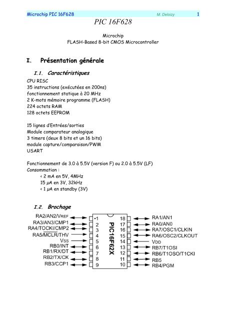
Microchip <strong>PIC</strong> <strong>16F628</strong> M. Deloizy 1<br />
<strong>PIC</strong> <strong>16F628</strong><br />
I..<br />
Microchip<br />
FLASH-Based 8-bit CMOS Microcontroller<br />
Présentation générale<br />
I.1. Caractéristiques<br />
CPU RISC<br />
35 instructions (exécutées en 200ns)<br />
fonctionnement statique à 20 MHz<br />
2 K-mots mémoire programme (FLASH)<br />
224 octets RAM<br />
128 octets EEPROM<br />
15 lignes d’Entrées/sorties<br />
Module comparateur analogique<br />
3 timers (deux 8 bits et un 16 bits)<br />
module capture/comparaison/PWM<br />
USART<br />
Fonctionnement de 3.0 à 5.5V (version F) ou 2.0 à 5.5V (LF)<br />
Consommation :<br />
< 2 mA en 5V, 4MHz<br />
15 µA en 3V, 32kHz<br />
< 1 µA en standby (3V)<br />
I.2. Brochage
Microchip <strong>PIC</strong> <strong>16F628</strong> M. Deloizy 2<br />
I.3. Description du brochage<br />
Name<br />
DIP<br />
Pin #<br />
I/O/P<br />
Type<br />
Buffer<br />
Type<br />
Description<br />
RA0/AN0 17 I/O ST Bi-directional I/O port/Analog comparator input<br />
RA1/AN1 18 I/O ST Bi-directional I/O port/Analog comparator input<br />
RA2/AN2/VREF 1 I/O ST Bi-directional I/O port/Analog comparator input/VREF out-put<br />
RA3/AN3/CMP1 2 I/O ST<br />
RA4/T0CKI/CMP2 3 I/O ST<br />
RA5/MCLR/THV 4 I ST<br />
RA6/OSC2/CLKOUT 15 I/O ST<br />
Bi-directional I/O port/Analog comparator input/comparator<br />
output<br />
Bi-directional I/O port/Can be configured as T0CKI/comparator<br />
output<br />
Input port/master clear (reset input/programming voltage input.<br />
When configured as MCLR, this pin is an active low reset to the<br />
device. Voltage on MCLR/THV must not exceed VDD during<br />
normal device operation.<br />
Bi-directional I/O port/Oscillator crystal output. Connects to<br />
crystal or resonator in crystal oscillator mode. In ER mode,<br />
OSC2 pin outputs CLKOUT which has 1/4 the frequency of OSC1,<br />
and denotes the instruction cycle rate.<br />
RA7/OSC1/CLKIN 16 I/O ST<br />
Bi-directional I/O port/Oscillator crystal input/external clock<br />
source input. ER biasing pin.<br />
RB0/INT 6 I/O<br />
(1) Bi-directional I/O port/external interrupt. Can be software<br />
TTL/ST<br />
programmed for internal weak pull-up.<br />
RB1/RX/DT 7 I/O<br />
(3) Bi-directional I/O port/ USART receive pin/synchronous data<br />
TTL/ST<br />
I/O. Can be software programmed for internal weak pull-up.<br />
RB2/TX/CK 8 I/O<br />
(3) Bi-directional I/O port/ USART transmit pin/synchronous clock<br />
TTL/ST<br />
I/O. Can be software programmed for internal weak pull-up.<br />
RB3/CCP1 9 I/O<br />
(4) Bi-directional I/O port/Capture/Compare/PWM I/O. Can be<br />
TTL/ST<br />
software programmed for internal weak pull-up.<br />
RB4/PGM 10 I/O TTL/ST (5)<br />
Bi-directional I/O port/Low voltage programming input pin.<br />
Wake-up from SLEEP on pin change. Can be software<br />
programmed for internal weak pull-up. When low voltage<br />
programming is enabled, the interrupt on pin change and weak<br />
pull-up resistor are disabled<br />
RB5 11 I/O TTL<br />
Bi-directional I/O port/Wake-up from SLEEP on pin change. Can<br />
be software programmed for internal weak pull-up.<br />
RB6/T1OSO/T1CKI 12 I/O TTL/ST (2)<br />
Bi-directional I/O port/Timer1 oscillator output/Timer1 clock<br />
input. Wake up from SLEEP on pin change. Can be software<br />
programmed for internal weak pull-up.<br />
RB7/T1OSI 13 I/O TTL/ST (2)<br />
Bi-directional I/O port/Timer1 oscillator input. Wake up from<br />
SLEEP on pin change. Can be software programmed for internal<br />
weak pull-up.<br />
VSS 5 P — Ground reference for logic and I/O pins.<br />
VDD 14 P — Positive supply for logic and I/O pins.<br />
Legend:<br />
O = output I/O = input/output P = power — = Not used<br />
I = Input ST = Schmitt Trigger input TTL = TTL input I/OD =input/open drain<br />
output<br />
Note 1: This buffer is a Schmitt Trigger input when configured as the external interrupt.<br />
Note 2: This buffer is a Schmitt Trigger input when used in serial programming mode.<br />
Note 3: This buffer is a Schmitt Trigger I/O when used in USART/Synchronous mode.<br />
Note 4: This buffer is a Schmitt Trigger I/O when used in CCP mode.<br />
Note 5: This buffer is a Schmitt Trigger input when used in low voltage program mode.
Microchip <strong>PIC</strong> <strong>16F628</strong> M. Deloizy 3<br />
II..<br />
Architecture interne<br />
→ Architecture Harvard<br />
mémoire données 8 bits<br />
mémoire programme 14 bits<br />
SFRs en mémoire de données.<br />
ALU 8 bits<br />
1 registre de travail (W : working reg.) 8 bits<br />
flags du registre STATUS associés à ALU :<br />
C (Carry)<br />
DC (Digit Carry)<br />
Z (Zero)<br />
Pile sur 8 niveaux
Microchip <strong>PIC</strong> <strong>16F628</strong> M. Deloizy 4<br />
II.1. Organisation mémoire<br />
II.1.a. Mémoire programme<br />
2 k-mots de 14 bits (0000h-07FFh)<br />
cyclique ⇒ 0800h ≈ 0000h<br />
PC 13 bits<br />
Vecteur Reset en 0000h<br />
Vecteur d’iT en 0004h<br />
II.1.b. Pile<br />
Non implantée dans les plans mémoire<br />
Accessible par instructions spécifiques<br />
→ CALL, RETURN, RETFIE, RETLW<br />
8 niveaux (structure de buffer circulaire)<br />
II.1.c. Mémoire de données<br />
→ 4 banques de 128 octets (00h-7Fh)<br />
contient SFRs (32 premiers octets de chaque banque)<br />
Registres à usage général (RAM statique) :<br />
020h-07Fh<br />
0A0h-0FFh<br />
120h-14Fh<br />
170h-17Fh<br />
1F0h-1FFh<br />
Mémoire commune (16 octets en ad. hautes) dans chaque banque<br />
→ visible en 70h-7Fh
Microchip <strong>PIC</strong> <strong>16F628</strong> M. Deloizy 5<br />
Plan mémoire :
Microchip <strong>PIC</strong> <strong>16F628</strong> M. Deloizy 6<br />
II.1.d. SFRs<br />
♦ STATUS<br />
→ registre d’état du processeur<br />
bit 7: IRP: Register Bank Select bit (used for indirect addressing)<br />
1 = Bank 2, 3 (100h - 1FFh)<br />
0 = Bank 0, 1 (00h - FFh)<br />
bit 6-5: RP1:RP0: Register Bank Select bits (used for direct addressing)<br />
11 = Bank 3 (180h - 1FFh)<br />
10 = Bank 2 (100h - 17Fh)<br />
01 = Bank 1 (80h - FFh)<br />
00 = Bank 0 (00h - 7Fh)<br />
bit 4: TO: Time-out bit<br />
1 = After power-up, CLRWDT instruction, or SLEEP instruction<br />
0 = A WDT time-out occurred<br />
bit 3: PD: Power-down bit<br />
1 = After power-up or by the CLRWDT instruction<br />
0 = By execution of the SLEEP instruction<br />
bit 2: Z: Zero bit<br />
1 = The result of an arithmetic or logic operation is zero<br />
0 = The result of an arithmetic or logic operation is not zero<br />
bit 1: DC: Digit carry/borrow bit (ADDWF, ADDLW,SUBLW,SUBWF<br />
instructions) (for borrow the polarity is reversed)<br />
1 = A carry-out from the 4th low order bit of the result occurred<br />
0 = No carry-out from the 4th low order bit of the result<br />
bit 0: C: Carry/borrow bit (ADDWF, ADDLW,SUBLW,SUBWF instructions)<br />
1 = A carry-out from the most significant bit of the result occurred<br />
0 = No carry-out from the most significant bit of the result occurred<br />
Note: For borrow the polarity is reversed. A subtraction is executed by adding<br />
the two’s complement of the second operand. For rotate (RRF, RLF) instructions,<br />
this bit is loaded with either the high or low order bit of the source register.
Microchip <strong>PIC</strong> <strong>16F628</strong> M. Deloizy 7<br />
♦ OPTION<br />
→ registre de configuration<br />
bit 7: RBPU: PORTB Pull-up Enable bit<br />
1 = PORTB pull-ups are disabled<br />
0 = PORTB pull-ups are enabled by individual port latch values<br />
bit 6: INTEDG: Interrupt Edge Select bit<br />
1 = Interrupt on rising edge of RB0/INT pin<br />
0 = Interrupt on falling edge of RB0/INT pin<br />
bit 5: T0CS: TMR0 Clock Source Select bit<br />
1 = Transition on RA4/T0CKI pin<br />
0 = Internal instruction cycle clock (CLKOUT)<br />
bit 4: T0SE: TMR0 Source Edge Select bit<br />
1 = Increment on high-to-low transition on RA4/T0CKI pin<br />
0 = Increment on low-to-high transition on RA4/T0CKI pin<br />
bit 3: PSA: Prescaler Assignment bit<br />
1 = Prescaler is assigned to the WDT<br />
0 = Prescaler is assigned to the Timer0 module<br />
bit 2-0: PS2:PS0: Prescaler Rate Select bits<br />
Bit Value TMR0 Rate WDT Rate<br />
000 1 : 2 1 : 1<br />
001 1 : 4 1 : 2<br />
010 1 : 8 1 : 4<br />
011 1 : 16 1 : 8<br />
100 1 : 32 1 : 16<br />
101 1 : 64 1 : 32<br />
110 1 : 128 1 : 64<br />
111 1 : 256 1 : 128
Microchip <strong>PIC</strong> <strong>16F628</strong> M. Deloizy 8<br />
♦ INTCON<br />
→ Autorisation des interruptions<br />
bit 7: GIE: Global Interrupt Enable bit<br />
1 = Enables all un-masked interrupts<br />
0 = Disables all interrupts<br />
bit 6: PEIE: Peripheral Interrupt Enable bit<br />
1 = Enables all un-masked peripheral interrupts<br />
0 = Disables all peripheral interrupts<br />
bit 5: T0IE: TMR0 Overflow Interrupt Enable bit<br />
1 = Enables the TMR0 interrupt<br />
0 = Disables the TMR0 interrupt<br />
bit 4: INTE: RB0/INT External Interrupt Enable bit<br />
1 = Enables the RB0/INT external interrupt<br />
0 = Disables the RB0/INT external interrupt<br />
bit 3: RBIE: RB Port Change Interrupt Enable bit<br />
1 = Enables the RB port change interrupt<br />
0 = Disables the RB port change interrupt<br />
bit 2: T0IF: TMR0 Overflow Interrupt Flag bit<br />
1 = TMR0 register has overflowed (must be cleared in software)<br />
0 = TMR0 register did not overflow<br />
bit 1: INTF: RB0/INT External Interrupt Flag bit<br />
1 = The RB0/INT external interrupt occurred (must be cleared in<br />
software)<br />
0 = The RB0/INT external interrupt did not occur<br />
bit 0: RBIF: RB Port Change Interrupt Flag bit<br />
1 = When at least one of the RB7:RB4 pins changed state (must be<br />
cleared in software)<br />
0 = None of the RB7:RB4 pins have changed state
Microchip <strong>PIC</strong> <strong>16F628</strong> M. Deloizy 9<br />
♦ PIE1<br />
→ Autorisation des interruptions<br />
bit 7: EEIE: EE Write Complete Interrupt Enable Bit<br />
1 = Enables the EE write complete interrupt<br />
0 = Disables the EE write complete interrupt<br />
bit 6: CMIE: Comparator Interrupt Enable bit<br />
1 = Enables the comparator interrupt<br />
0 = Disables the comparator interrupt<br />
bit 5: RCIE: USART Receive Interrupt Enable bit<br />
1 = Enables the USART receive interrupt<br />
0 = Disables the USART receive interrupt<br />
bit 4: TXIE: USART Transmit Interrupt Enable bit<br />
1 = Enables the USART transmit interrupt<br />
0 = Disables the USART transmit interrupt<br />
bit 3: Unimplemented: Read as ‘0’<br />
bit 2: CCP1IE: CCP1 Interrupt Enable bit<br />
1 = Enables the CCP1 interrupt<br />
0 = Disables the CCP1 interrupt<br />
bit 1: TMR2IE: TMR2 to PR2 Match Interrupt Enable bit<br />
1 = Enables the TMR2 to PR2 match interrupt<br />
0 = Disables the TMR2 to PR2 match interrupt<br />
bit 0: TMR1IE: TMR1 Overflow Interrupt Enable bit<br />
1 = Enables the TMR1 overflow interrupt<br />
0 = Disables the TMR1 overflow interrupt
Microchip <strong>PIC</strong> <strong>16F628</strong> M. Deloizy 10<br />
♦ PIR1<br />
→ Registre d’indicateurs d’interruptions reçues<br />
bit 7: EEIF: EEPROM Write Operation Interrupt Flag bit<br />
1 = The write operation completed (must be cleared in software)<br />
0 = The write operation has not completed or has not been started<br />
bit 6: CMIF: Comparator Interrupt Flag bit<br />
1 = Comparator input has changed<br />
0 = Comparator input has not changed<br />
bit 5: RCIF: USART Receive Interrupt Flag bit<br />
1 = The USART receive buffer is full<br />
0 = The USART receive buffer is empty<br />
bit 4: TXIF: USART Transmit Interrupt Flag bit<br />
1 = The USART transmit buffer is empty<br />
0 = The USART transmit buffer is full<br />
bit 3: Unimplemented: Read as ‘0’<br />
bit 2: CCP1IF: CCP1 Interrupt Flag bit<br />
Capture Mode<br />
1 = A TMR1 register capture occurred (must be cleared in software)<br />
0 = No TMR1 register capture occurred<br />
Compare Mode<br />
1 = A TMR1 register compare match occurred (must be cleared in<br />
software)<br />
0 = No TMR1 register compare match occurred<br />
PWM Mode<br />
Unused in this mode<br />
bit 1: TMR2IF: TMR2 to PR2 Match Interrupt Flag bit<br />
1 = TMR2 to PR2 match occurred (must be cleared in software)<br />
0 = No TMR2 to PR2 match occurred<br />
bit 0: TMR1IF: TMR1 Overflow Interrupt Flag bit<br />
1 = TMR1 register overflowed (must be cleared in software)<br />
0= TMR1 register did not overflow
Microchip <strong>PIC</strong> <strong>16F628</strong> M. Deloizy 11<br />
♦ PCON<br />
→ registre de configuration<br />
bit 7-4,2:Unimplemented: Read as '0'<br />
bit 3: OSCF: INTRC/ER oscillator speed<br />
1 = 4 MHz typical (1)<br />
0 = 37 KHz typical<br />
bit 1: POR: Power-on Reset Status bit<br />
1 = No Power-on Reset occurred<br />
0 = A Power-on Reset occurred (must be set in software after a Poweron<br />
Reset occurs)<br />
bit 0: BOD: Brown-out Detect Status bit<br />
1 = No Brown-out Reset occurred<br />
0 = A Brown-out Reset occurred (must be set in software after a Brownout<br />
Reset occurs)<br />
Note 1: When in ER oscillator mode, setting OSCF = 1 will cause the oscillator<br />
speed to change to the speed specified by the external resistor.<br />
♦ PCL et PCLATH<br />
→ constitution de PC (13 bits)
Microchip <strong>PIC</strong> <strong>16F628</strong> M. Deloizy 12<br />
♦ INDF et FSR<br />
→ Adressage indirect<br />
FSR contient l’adresse de la donnée<br />
L’opération de lecture ou d’écriture sur INDF porte en réalité sur la donnée<br />
pointée par FSR.<br />
Exemple : effacement de la mémoire 20h à 2Fh<br />
movlw 0x20 ;initialize pointer<br />
movwf FSR ;to RAM<br />
NEXT: clrf INDF ;clear INDF register<br />
incf FSR ;inc pointer<br />
btfss FSR,4 ;all done?<br />
goto NEXT ;no clear next<br />
;yes continue<br />
CONTINUE:
Microchip <strong>PIC</strong> <strong>16F628</strong> M. Deloizy 13<br />
II.2. Mémoire EEPROM<br />
→ Permet de sauvegarder des données (mémoire non volatile)<br />
→ Ecritures/lectures non « instantanées »<br />
II.2.a. EEDATA :<br />
→ Contient la donnée lue ou à écrire<br />
II.2.b. EEADR :<br />
→Indique l’adresse de la donnée<br />
bit 7 Unimplemented Address: Must be set to '0'<br />
bit 6:0 EEADR: Specifies one of 128 locations for EEPROM Read/Write<br />
Operation<br />
II.2.c. EECON1 :<br />
→ Indique le type d’opération à réaliser.<br />
bit 7:4 Unimplemented: Read as '0'<br />
bit 3 WRERR: EEPROM Error Flag bit<br />
1 = A write operation is prematurely terminated<br />
(any MCLR reset, any WDT reset during normal operation or<br />
BOD detect)<br />
0 = The write operation completed<br />
bit 2 WREN: EEPROM Write Enable bit<br />
1 = Allows write cycles<br />
0 = Inhibits write to the data EEPROM<br />
bit 1 WR: Write Control bit<br />
1 = initiates a write cycle. (The bit is cleared by hardware once write is<br />
complete. The WR bit can only be set (not cleared) in software.<br />
0 = Write cycle to the data EEPROM is complete<br />
bit 0 RD: Read Control bit<br />
1 = Initiates an EEPROM read (read takes one cycle. RD is cleared in<br />
hardware. The RD bit can only be set (not cleared) in software).<br />
0 = Does not initiate an EEPROM read
Microchip <strong>PIC</strong> <strong>16F628</strong> M. Deloizy 14<br />
III..<br />
Fonctionnements spéciaux<br />
III.1. Mot de configuration<br />
→ Accessible uniquement en phase de programmation (électrique)
Microchip <strong>PIC</strong> <strong>16F628</strong> M. Deloizy 15<br />
III.2. Oscillateur<br />
III.2.a. Oscillateur à quartz (ou résonateurs céramiques)<br />
III.2.b. Horloge externe<br />
III.2.c. Oscillateur externe<br />
→ Il est préférable d’utiliser un oscillateur intégré (plus stable).<br />
III.2.d. Résistance externe<br />
III.2.e. RC interne<br />
→ Pour applications ne nécessitant pas une grande<br />
précision temporelle.<br />
La résistance doit être comprise entre 38k et 1MΩ<br />
Fournit une horloge entre 10kHz et 8MHz<br />
Fournit en interne un oscillateur à 4MHz (5V / 25°C)
Microchip <strong>PIC</strong> <strong>16F628</strong> M. Deloizy 16<br />
III.3. Démarrage du système<br />
6 possibilités au démarrage du système :<br />
• Power on reset (POR)<br />
→ mise sous tension du système<br />
• MCLR activé pendant fonctionnement normal<br />
• MCLR activé pendant mode SLEEP<br />
• Watchdog pendant fonctionnement normal<br />
• Watchdog pendant le mode SLEEP<br />
• Chute de la tension d’alimentation (Brown-Out Detect)<br />
→ quand Vcc tombe en dessous de 4V.<br />
Configurations possibles (flags de STATUS & PCON)<br />
POR BOD TO PD<br />
0 x 1 1 Power-on-reset<br />
1 0 x x Brown-out Detect<br />
1 1 0 u WDT Reset<br />
1 1 0 0 WDT Wake-up<br />
1 1 u u MCLR reset during normal operation<br />
1 1 1 0 MCLR reset during SLEEP<br />
Legend: u = unchanged, x = unknown<br />
III.4. Interruptions<br />
Sources d’interruptions :<br />
Interruption externe RB0/INT Changement sur PortB (RB7 :RB4)<br />
TMR0 overflow Comparateur<br />
TMR1 overflow USART<br />
TMR2 match CCP<br />
Masquages individuals et masquage global dans INTCON.<br />
Quand iT demandée :<br />
• GIE (Global Interrupt Enable) mis à 0 (interdit autres iT)<br />
• Adresse de retour empilée<br />
• PC chargé avec 0004h<br />
• … sauvegarder W et STATUS (pas dans la pile !)<br />
• … vérification de la source d’iT<br />
• … traitement de l’iT<br />
• … acquittement de l’iT par remise à 0 des flags d’iT<br />
• RETFIE → termine la routine d’iT (et remet GIE à 1).
Microchip <strong>PIC</strong> <strong>16F628</strong> M. Deloizy 17<br />
Sauvegarde de W et STATUS en RAM :<br />
MOVWF W_TEMP ;copy W to temp register, could be in either bank<br />
SWAPF STATUS,W ;swap status to be saved into W<br />
BCF STATUS,RP0 ;change to bank 0 regardless of current bank<br />
MOVWF ST_TEMP ;save status to bank 0 register<br />
:<br />
: (ISR)<br />
:<br />
SWAPF ST_TEMP,W ;swap ST_TEMP register into W,<br />
;sets bank to original state<br />
MOVWF STATUS ;move W into STATUS register<br />
SWAPF W_TEMP,F ;swap W_TEMP<br />
SWAPF W_TEMP,W ;swap W_TEMP into W<br />
III.5. Watchdog<br />
→ compteur indépendant.<br />
Durée ≈ 18ms sans prédiviseur d’horloge (jusqu’à 2,3s avec)<br />
Activé par WDTE du mot de configuration<br />
Fonctionne même si horloge arrêtée (sur OSC1, OSC2) par SLEEP.<br />
En mode normal → déclenchement d’un RESET<br />
En mode SLEEP → réveil du µP → retour au fonctionnement normal.<br />
CLRWDT et SLEEP initialisent le watchdog<br />
III.6. Mode Power-down<br />
→ atteint par l’instruction SLEEP<br />
→ arrête le driver de l’oscillateur (arrêt de l’horloge)<br />
Réveil par :<br />
• MCLR → Réinitialisation du système<br />
• Watchdog<br />
• Interruption sur RB0/INT ou RB change ou comparateur<br />
Poursuite du<br />
programme
Microchip <strong>PIC</strong> <strong>16F628</strong> M. Deloizy 18<br />
III.7. Programmation électrique<br />
Programmation de type série<br />
- horloge<br />
- donnée<br />
- tension de programmation<br />
- alimentations (5V, GND)<br />
2 possibilités :<br />
♦ avec tension de programmation<br />
RB6 & RB7 maintenus à 0 pendant que Vpp passe de 0 à VIHH (VDD+3,5 à 13,5V)<br />
♦ en basse tension (5V)<br />
bit LVP du mot de configuration mis à 1.<br />
Mode programmation atteint quand RB4=1 (interdit utilisation de RB4 en E/S)<br />
LVP peut être mis à 1 en mode « haute tension » (ce mode est toujours<br />
disponible).
Microchip <strong>PIC</strong> <strong>16F628</strong> M. Deloizy 19<br />
IV..<br />
Programmation logicielle<br />
IV.1. Ecriture de programmes<br />
IV.1.a. Instructions sur octets<br />
'f' : registre (file register), de 0 à 7Fh<br />
'd' : destination<br />
si d=0 → résultat dans W<br />
si d=1 → résultat dans 'f'<br />
Exemples :<br />
CLRW 0 → W<br />
DECF CNT,1 CNT-1 → CNT<br />
DECF CNT,0 CNT-1 → W<br />
ENCORE DECFSZ REG,1 décrémente REG ; SKIP * si Zéro<br />
GOTO ENCORE brancher à ENCORE si REG ≠ 0<br />
SUITE<br />
f défini = 1<br />
SWAP RG1,f si RG1=F4h ⇒ RG1=4Fh<br />
SUBWF AB,W AB-W → W ; C=1 si résultat ≥ 0<br />
W défini = 0<br />
(*) : n'exécute pas l'instruction suivante.<br />
IV.1.b. Instructions sur bits<br />
'b' : numéro du bit affecté par l'opération (0 à 7)<br />
'f' : registre<br />
Exemples :<br />
BCF REG,3 met à 0 le bit 3 de REG<br />
BTFSC CNT,7 test du bit 7 de CNT ; SKIP si = 0<br />
IV.1.c. Opérations littérales et de contrôle<br />
'k' : constante de 8 ou 11 bits, ou valeur littérale<br />
Exemples :<br />
ADDLW 23 W+23 → W ; k sur 8 bits<br />
CALL TOTO appel du sous pgm TOTO ; k sur 11 bits<br />
GOTO SUITE<br />
MOVLW 0x03 03h → W<br />
CLRWDT remise à 0 du Watchdog<br />
SLEEP mise en veille (réveil par RESET, iT ou WDT)<br />
RETLW 0x12 ⇔ W=12h ; RETURN
Microchip <strong>PIC</strong> <strong>16F628</strong> M. Deloizy 20<br />
Utilisation de RETLW (lecture d'une donnée en mémoire programme) :<br />
MOVLW 5<br />
CALL TABLE<br />
………..<br />
TABLE ADDWF PC<br />
RETLW CT1 CT1 : valeur retournée si W=1<br />
RETLW CT2 CT2 : valeur retournée si W=2<br />
RETLW CT3 CT3 : valeur retournée si W=3<br />
………..
Microchip <strong>PIC</strong> <strong>16F628</strong> M. Deloizy 21<br />
IV.2. Jeu d’instructions<br />
Mnemonic, Description Cycles 14-Bit<br />
Opcode<br />
Status Notes<br />
Operands Affected<br />
MSb LSb<br />
BYTE-ORIENTED FILE REGISTER OPERATIONS<br />
ADDWF f, d Add W and f 1 00 0111 dfff ffff C,DC,Z 1,2<br />
ANDWF f, d AND W with f 1 00 0101 dfff ffff Z 1,2<br />
CLRF f Clear f 1 00 0001 lfff ffff Z 2<br />
CLRW - Clear W 1 00 0001 0xxx xxxx Z<br />
COMF f, d Complement f 1 00 1001 dfff ffff Z 1,2<br />
DECF f, d Decrement f 1 00 0011 dfff ffff Z 1,2<br />
DECFSZ f, d Decrement f, Skip if 0 1(2) 00 1011 dfff ffff 1,2,3<br />
INCF f, d Increment f 1 00 1010 dfff ffff Z 1,2<br />
INCFSZ f, d Increment f, Skip if 0 1(2) 00 1111 dfff ffff 1,2,3<br />
IORWF f, d Inclusive OR W with f 1 00 0100 dfff ffff Z 1,2<br />
MOVF f, d Move f 1 00 1000 dfff ffff Z 1,2<br />
MOVWF f Move W to f 1 00 0000 lfff ffff<br />
NOP - No Operation 1 00 0000 0xx0 0000<br />
RLF f, d Rotate Left f through Carry 1 00 1101 dfff ffff C 1,2<br />
RRF f, d Rotate Right f through Carry 1 00 1100 dfff ffff C 1,2<br />
SUBWF f, d Subtract W from f 1 00 0010 dfff ffff C,DC,Z 1,2<br />
SWAPF f, d Swap nibbles in f 1 00 1110 dfff ffff 1,2<br />
XORWF f, d Exclusive OR W with f 1 00 0110 dfff ffff Z 1,2<br />
BIT-ORIENTED FILE REGISTER OPERATIONS<br />
BCF f, b Bit Clear f 1 01 00bb bfff ffff 1,2<br />
BSF f, b Bit Set f 1 01 01bb bfff ffff 1,2<br />
BTFSC f, b Bit Test f, Skip if Clear 1 (2) 01 10bb bfff ffff 3<br />
BTFSS f, b Bit Test f, Skip if Set 1 (2) 01 11bb bfff ffff 3<br />
LITERAL AND CONTROL OPERATIONS<br />
ADDLW k Add literal and W 1 11 111x kkkk kkkk C,DC,Z<br />
ANDLW k AND literal with W 1 11 1001 kkkk kkkk Z<br />
CALL k Call subroutine 2 10 0kkk kkkk kkkk<br />
CLRWDT - Clear Watchdog Timer 1 00 0000 0110 0100 TO,PD<br />
GOTO k Go to address 2 10 1kkk kkkk kkkk<br />
IORLW k Inclusive OR literal with W 1 11 1000 kkkk kkkk Z<br />
MOVLW k Move literal to W 1 11 00xx kkkk kkkk<br />
RETFIE - Return from interrupt 2 00 0000 0000 1001<br />
RETLW k Return with literal in W 2 11 01xx kkkk kkkk<br />
RETURN - Return from Subroutine 2 00 0000 0000 1000<br />
SLEEP - Go into standby mode 1 00 0000 0110 0011 TO,PD<br />
SUBLW k Subtract W from literal 1 11 110x kkkk kkkk C,DC,Z<br />
XORLW k Exclusive OR literal with W 1 11 1010 kkkk kkkk Z
Microchip <strong>PIC</strong> <strong>16F628</strong> M. Deloizy 22<br />
V..<br />
Périphériques<br />
V.1. Ports d'entrées-sorties<br />
2 ports 8 bits : PORTA et PORTB<br />
direction contrôlée par TRISA et TRISB<br />
V.1.a. PORTA<br />
Particularités :<br />
entrées avec trigger de Schmitt<br />
RA4 sortie drain ouvert<br />
RA5 entrée seulement<br />
autres sorties avec drivers push-pull<br />
bits de TRISA :<br />
'1' : drivers de sortie en haute impédance<br />
'0' : drivers en basse impédance<br />
PORTA multiplexé avec :<br />
- comparateurs/références de tension (CMCON & VRCON)<br />
- oscillateur.<br />
- MCLR, VPP<br />
Exemple d'initialisation<br />
CLRF PORTA ;Initialize PORTA by<br />
;setting output data latches<br />
MOVLW 0x07 ;Turn comparators off and<br />
MOVWF CMCON ;enable pins for I/O functions<br />
BCF STATUS,RP1<br />
BSF STATUS,RP0 ;Select Bank1<br />
MOVLW 0x1F ;Value used to initialize<br />
;data direction<br />
MOVWF TRISA ;Set RA as inputs<br />
;TRISA always read as ‘1’.<br />
;TRISA depend on oscillator mode
Microchip <strong>PIC</strong> <strong>16F628</strong> M. Deloizy 23<br />
V.1.b. PORTB<br />
8 bits bidirectionnel<br />
Possibilité tirage haut interne (OPTION.7) (≈200µA)<br />
bits de TRISB :<br />
'1' : drivers de sortie en haute impédance<br />
'0' : drivers en basse impédance<br />
PORTB multiplexé avec :<br />
- interruption externe, USART, CCP, TIMER1 in/out<br />
Possibilité de déclencher iT sur changement d'état sur RB.7 à RB.4<br />
V.2. USART<br />
(UNIVERSAL SYNCHRONOUS/ASYNCHRONOUS RECEIVER/TRANSMITTER)<br />
Communication série synchrone ou asynchrone<br />
sur pattes RB2/TX/CK and RB1/RX/DT<br />
contrôlé par :<br />
- TXSTA : état et contrôle de la transmission<br />
- RCSTA : état et contrôle de la réception<br />
- SPBRG : générateur de bauds<br />
module d'émission :<br />
module de réception :
Microchip <strong>PIC</strong> <strong>16F628</strong> M. Deloizy 24<br />
V.2.a. TXSTA: TRANSMIT STATUS AND CONTROL REGISTER<br />
bit 7 CSRC: Clock Source Select bit<br />
Asynchronous mode : Don’t care<br />
Synchronous mode :<br />
1 = Master mode (Clock generated internally from BRG)<br />
0 = Slave mode (Clock from external source)<br />
bit 6 TX9: 9-bit Transmit Enable bit<br />
1 = Selects 9-bit transmission<br />
0 = Selects 8-bit transmission<br />
bit 5 TXEN: Transmit Enable bit(1)<br />
1 = Transmit enabled<br />
0 = Transmit disabled<br />
bit 4 SYNC: USART Mode Select bit<br />
1 = Synchronous mode<br />
0 = Asynchronous mode<br />
bit 3 Unimplemented: Read as '0'<br />
bit 2 BRGH: High Baud Rate Select bit<br />
Asynchronous mode :<br />
1 = High speed<br />
0 = Low speed<br />
Synchronous mode : Unused in this mode<br />
bit 1 TRMT: Transmit Shift Register STATUS bit<br />
1 = TSR empty<br />
0 = TSR full<br />
bit 0 TX9D: 9th bit of transmit data.<br />
Can be PARITY bit.<br />
Note 1: SREN/CREN overrides TXEN in SYNC mode.
Microchip <strong>PIC</strong> <strong>16F628</strong> M. Deloizy 25<br />
V.2.b. RCSTA: RECEIVE STATUS AND CONTROL REGISTER<br />
bit 7 SPEN: Serial Port Enable bit<br />
(Configures RB1/RX/DT and RB2/TX/CK pins as serial port pins<br />
when bits TRISB are set)<br />
1 = Serial port enabled<br />
0 = Serial port disabled<br />
bit 6 RX9: 9-bit Receive Enable bit<br />
1 = Selects 9-bit reception<br />
0 = Selects 8-bit reception<br />
bit 5 SREN: Single Receive Enable bit<br />
Asynchronous mode: Don’t care<br />
Synchronous mode :<br />
- master: (This bit is cleared after reception is complete)<br />
1 = Enables single receive<br />
0 = Disables single receive<br />
- slave: Unused in this mode<br />
bit 4 CREN: Continuous Receive Enable bit<br />
Asynchronous mode: 1 = Enables continuous receive<br />
0 = Disables continuous receive<br />
Synchronous mode: 1 = Enables continuous receive until<br />
enable bit CREN is cleared (CREN overrides SREN)<br />
0 = Disables continuous receive<br />
bit 3 ADEN: Address Detect Enable bit<br />
Asynchronous mode 9-bit (RX9 = 1):<br />
1 = Enables address detection, enable interrupt and load of<br />
the receive buffer when RSR is set<br />
0 = Disables address detection, all bytes are received, and<br />
ninth bit can be used as PARITY bit<br />
Asynchronous mode 8-bit (RX9=0) : Unused in this mode<br />
Synchronous mode : Unused in this mode<br />
bit 2 FERR: Framing Error bit<br />
1 = Framing error (Can be updated by reading RCREG<br />
register and receive next valid byte)<br />
0 = No framing error<br />
bit 1 OERR: Overrun Error bit<br />
1 = Overrun error (Can be cleared by clearing bit CREN)<br />
0 = No overrun error<br />
bit 0 RX9D: 9th bit of received data (Can be PARITY bit)
Microchip <strong>PIC</strong> <strong>16F628</strong> M. Deloizy 26<br />
V.2.c. Générateur de Bauds<br />
contrôlé par :<br />
- SPBRG (registre 8 bits) (valeurs 0 à 255)<br />
- BRGH (TXSTA.2)<br />
Mode synchrone :<br />
Fosc<br />
Baud =<br />
avec BRGH = 0<br />
4 ⋅ SPBRG +<br />
Mode asynchrone :<br />
( 1)<br />
Fosc<br />
Baud =<br />
(BRGH = 0)<br />
64 ⋅(<br />
SPBRG + 1)<br />
Fosc<br />
Baud =<br />
(BRGH = 1)<br />
16 ⋅ SPBRG + 1<br />
( )<br />
pour réduire l'erreur, il est préférable de prendre BRGH = 1<br />
Exemple :<br />
si Fosc = 4MHz<br />
On veut 9600 bauds :<br />
BRGH Baud min Baud max<br />
0 244 62 500<br />
1 977 250 000<br />
BRGH SPBRG calculé SPBRG arrondi BAUDS obtenus Erreur<br />
0 5,51 6 8928,6 7 %<br />
1 25,04 25 9615,4 0,1 %
Microchip <strong>PIC</strong> <strong>16F628</strong> M. Deloizy 27<br />
VI..<br />
Annexes<br />
VI.1. Notes d'applications<br />
Description Documentation<br />
<strong>PIC</strong>16C5x/<strong>PIC</strong>16Cxx Utility Math Routines AN526<br />
51097a<br />
Source Code<br />
Using PWM to Generate Analog Output AN538<br />
Software Implementation of I²C Bus Master AN554 Source Code<br />
Implementing a Table Read AN556<br />
Using the Port B Interrupt on Change as an External<br />
Interrupt<br />
AN566<br />
Macros for Page and Bank Switching AN586 Source Code<br />
Interfacing <strong>PIC</strong>micros to an LCD Module AN587 Source Code<br />
Adaptive Differential Pulse Code Modulation using the AN643 Source Code<br />
<strong>PIC</strong>16/17<br />
PWM, A Software Solution using the 16CXXX Devices AN654<br />
<strong>PIC</strong>18CXXX/<strong>PIC</strong>16CXXX DC Servomotor AN696 Source Code<br />
IEEE 754 Compliant Floating Point Routines AN575 Source Code<br />
Techniques to Disable Global Interrupts AN576<br />
<strong>PIC</strong>16/17 Oscillator Design Guide AN588<br />
Low Power Design Using <strong>PIC</strong>16/17 AN606<br />
Using Timer 1 in Asynchronous Clock Mode AN580<br />
Low-Power Real Time Clock AN582 Source Code<br />
A Real-Time Operating System for <strong>PIC</strong>16/17 AN585 Source Code<br />
Using the CCP Modules AN594 Source Code<br />
Improving the Susceptibility of an Application to ESD AN595<br />
Implementing Ultrasonic Ranging AN597 Source Code<br />
Power-up Trouble Shooting AN607 Source Code<br />
Fixed Point Routines AN617 Source Code<br />
D/A Conversion Using PWM and R-2R Ladders to<br />
Generate Sine and DTMF Waveforms<br />
AN655 Source Code<br />
In-Circuit Serial Programming of Calibration Parameters AN656 Source Code<br />
Using a <strong>PIC</strong>micro® Microcontroller<br />
Floating Point Routines AN660 Source Code<br />
CRC Generating and Checking AN730 Source Code<br />
Automatic Calibration of the WDT Time-out Period 91003a<br />
TechBrief: Using SRAM with a <strong>PIC</strong>16CXX 91011a<br />
How to Implement ICSP Using <strong>PIC</strong>16CXXX OTP<br />
MCUs<br />
91013b<br />
Using a <strong>PIC</strong>16F877 To Develop Code for <strong>PIC</strong>16CXXX 91033a<br />
Devices<br />
TechBrief Tranformerless Power Supply 91008b<br />
BASIC <strong>PIC</strong>16/17 OSCILLATOR DESIGN GUIDE fact001<br />
Low Frequency Magnetic Transmitter Design AN232
Microchip <strong>PIC</strong> <strong>16F628</strong> M. Deloizy 28<br />
VI.2. Fichier template<br />
Program Files\MPLAB IDE\MCHIP_Tools\TEMPLATE\Code\f628temp.asm<br />
list p=16f628 ; list directive to define processor<br />
#include ; processor specific variable definitions<br />
__CONFIG _CP_OFF & _WDT_ON & _BODEN_ON & _PWRTE_ON & _ER_OSC_CLKOUT &<br />
_MCLRE_ON & _LVP_ON<br />
; '__CONFIG' directive is used to embed configuration data within .asm file.<br />
; The lables following the directive are located in the respective .inc file.<br />
; See respective data sheet for additional information on configuration word.<br />
;***** VARIABLE DEFINITIONS<br />
w_temp EQU 0x70 ; variable used for context saving<br />
status_temp EQU 0x71 ; variable used for context saving<br />
;**********************************************************************<br />
ORG 0x000 ; processor reset vector<br />
goto main ; go to beginning of program<br />
ORG 0x004 ; interrupt vector location<br />
movwf w_temp ; save off current W register contents<br />
movf STATUS,w ; move status register into W register<br />
movwf status_temp ; save off contents of STATUS register<br />
; isr code can go here or be located as a call subroutine elsewhere<br />
main<br />
movf status_temp,w ; retrieve copy of STATUS register<br />
movwf STATUS ; restore pre-isr STATUS register contents<br />
swapf w_temp,f<br />
swapf w_temp,w ; restore pre-isr W register contents<br />
retfie ; return from interrupt<br />
; remaining code goes here<br />
END ; directive 'end of program'
Microchip <strong>PIC</strong> <strong>16F628</strong><br />
Table des matières<br />
M. Deloizy 29<br />
II. . Présentation générale ................................................................................................... 1<br />
I.1. Caractéristiques ..................................................................................................... 1<br />
I.2. Brochage................................................................................................................... 1<br />
I.3. Description du brochage ......................................................................................2<br />
IIII. . Architecture interne.................................................................................................3<br />
II.1. Organisation mémoire .......................................................................................4<br />
II.1.a. Mémoire programme......................................................................................4<br />
II.1.b. Pile .....................................................................................................................4<br />
II.1.c. Mémoire de données......................................................................................4<br />
II.1.d. SFRs ..................................................................................................................6<br />
II.2. Mémoire EEPROM ............................................................................................13<br />
II.2.a. EEDATA : .......................................................................................................13<br />
II.2.b. EEADR : ......................................................................................................13<br />
II.2.c. EECON1 :........................................................................................................13<br />
IIIIII. . Fonctionnements spéciaux .....................................................................................14<br />
III.1. Mot de configuration.......................................................................................14<br />
III.2. Oscillateur .........................................................................................................15<br />
III.2.a. Oscillateur à quartz (ou résonateurs céramiques)...........................15<br />
III.2.b. Horloge externe .......................................................................................15<br />
III.2.c. Oscillateur externe .................................................................................15<br />
III.2.d. Résistance externe..................................................................................15<br />
III.2.e. RC interne ..................................................................................................15<br />
III.3. Démarrage du système ...................................................................................16<br />
III.4. Interruptions ....................................................................................................16<br />
III.5. Watchdog...........................................................................................................17<br />
III.6. Mode Power-down.............................................................................................17<br />
III.7. Programmation électrique ..............................................................................18<br />
IIV. . Programmation logicielle.........................................................................................19<br />
IV.1. Ecriture de programmes.................................................................................19<br />
IV.1.a. Instructions sur octets ..............................................................................19<br />
IV.1.b. Instructions sur bits...................................................................................19<br />
IV.1.c. Opérations littérales et de contrôle.......................................................19<br />
IV.2. Jeu d’instructions ............................................................................................21<br />
V. . Périphériques................................................................................................................ 22<br />
V.1. Ports d'entrées-sorties..................................................................................... 22<br />
V.1.a. PORTA ........................................................................................................... 22<br />
V.1.b. PORTB............................................................................................................ 23<br />
V.2. USART................................................................................................................... 23<br />
V.2.a. TXSTA: TRANSMIT STATUS AND CONTROL REGISTER ........... 24<br />
V.2.b. RCSTA: RECEIVE STATUS AND CONTROL REGISTER ................. 25<br />
V.2.c. Générateur de Bauds.................................................................................. 26<br />
VII. . Annexes ..................................................................................................................... 27
Microchip <strong>PIC</strong> <strong>16F628</strong> M. Deloizy 30<br />
VI.1. Notes d'applications....................................................................................... 27<br />
VI.2. Fichier template.............................................................................................. 28