Drude conductivity of Dirac fermions in graphene - APS Link ...
Drude conductivity of Dirac fermions in graphene - APS Link ...
Drude conductivity of Dirac fermions in graphene - APS Link ...

You also want an ePaper? Increase the reach of your titles
YUMPU automatically turns print PDFs into web optimized ePapers that Google loves.
JASON HORNG et al. PHYSICAL REVIEW B 83, 165113 (2011)<br />
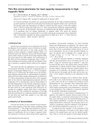
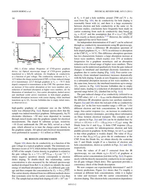
at V = 0 and a hole mobility around 2700 cm 2 /Vs.As<br />
-50 0<br />
(a)<br />
(b)<br />
5%. The sample had an <strong>in</strong>itial hole dop<strong>in</strong>g <strong>of</strong> 1.05 × 10 12 cm −2 electron dop<strong>in</strong>g. This electron-hole concentration dependence<br />
40<br />
g<br />
seen from Fig. 1(b), the dc <strong>conductivity</strong> for hole dop<strong>in</strong>g is<br />
30<br />
reasonably l<strong>in</strong>ear with |n|, and there is a large asymmetry<br />
between electron and hole <strong>conductivity</strong> at the same |n|. In<br />
20<br />
previous studies, conclusions have frequently been made on<br />
10<br />
carrier scatter<strong>in</strong>g from such dc <strong>conductivity</strong> data based on<br />
σ dc = D/πƔ and the assumption that D = (v F e 2 / ¯h) √ π|n|<br />
0<br />
holds exactly as theory predicts. 23–25 However, the validity <strong>of</strong><br />
50<br />
V g<br />
(V)<br />
100<br />
this approach has never been tested.<br />
5<br />
2E has two characteristic features: a large absorption <strong>in</strong>crease at<br />
F<br />
0<br />
lower wave numbers, which reaches over 15% at terahertz<br />
0 1500 3000 4500 6000<br />
frequencies for a <strong>graphene</strong> monolayer, and an absorption<br />
ω(cm -1 )<br />
reduction over a broad range <strong>of</strong> higher wave numbers. These<br />
(c)<br />
20<br />
(d)<br />
An <strong>in</strong>dependent determ<strong>in</strong>ation <strong>of</strong> D and Ɣ can be achieved<br />
through ac <strong>conductivity</strong> measurements us<strong>in</strong>g IR spectroscopy.<br />
15<br />
Figure 1(c) shows a difference IR absorption spectrum <strong>of</strong><br />
10<br />
hole-doped <strong>graphene</strong> (V g =−70 V) <strong>in</strong> reference to absorption<br />
at the CNP (V g = 14 V). This difference absorption spectrum<br />
features can be understood qualitatively from the gate-<strong>in</strong>duced<br />
FIG. 1. (Color onl<strong>in</strong>e) Properties <strong>of</strong> CVD-grown <strong>graphene</strong><br />
changes <strong>in</strong> <strong>in</strong>traband and <strong>in</strong>terband electronic transitions <strong>in</strong><br />
device. (a) Optical microscope image <strong>of</strong> CVD-grown <strong>graphene</strong><br />
<strong>graphene</strong> due to carrier dop<strong>in</strong>g [Fig. 1(d)]. Free-carrier <strong>conductivity</strong><br />
(from <strong>in</strong>traband transitions) <strong>in</strong>creases dramatically<br />
transferred to a SiO 2 /Si substrate. (b) Graphene dc <strong>conductivity</strong><br />
as a function <strong>of</strong> gate voltage. The <strong>conductivity</strong> m<strong>in</strong>imum at V g =<br />
with the hole dop<strong>in</strong>g. It peaks at zero frequency and gives rise<br />
14 V def<strong>in</strong>es the charge neutral po<strong>in</strong>t (CNP). (c) Gate-<strong>in</strong>duced change<br />
to a substantial absorption <strong>in</strong>crease at low wave numbers. At<br />
<strong>of</strong> ir transmittance T/T through <strong>graphene</strong> at V g =−70 V (hole<br />
doped) compared to transmittance at the CNP. The spectrum shows<br />
the same time, however, the <strong>in</strong>terband transitions up to energy<br />
an <strong>in</strong>crease <strong>of</strong> free-carrier absorption at low wave numbers and a 2E F [arrows <strong>in</strong> Fig. 1(d)] become forbidden due to empty<br />
reduction <strong>of</strong> <strong>in</strong>terband absorption at higher wave numbers. (d) An <strong>in</strong>itial states, lead<strong>in</strong>g to a reduction <strong>of</strong> absorption <strong>in</strong> the broad<br />
illustration <strong>of</strong> <strong>in</strong>traband (i.e., free-carrier absorption, dashed arrow) spectral range below 2E F [dashed l<strong>in</strong>e <strong>in</strong> Fig. 1(c)].<br />
and <strong>in</strong>terband (solid arrow) transitions <strong>in</strong> hole-doped <strong>graphene</strong>. The gate-<strong>in</strong>duced change <strong>of</strong> ac <strong>conductivity</strong> (referred to as<br />
Intraband absorption <strong>in</strong>creases with carrier dop<strong>in</strong>g, while <strong>in</strong>terband the CNP value), ˜σ = ˜σ − ˜σ CNP , can be obta<strong>in</strong>ed readily from<br />
transitions up to 2E F become forbidden due to empty <strong>in</strong>itial states, the difference IR absorption spectra (see auxiliary material).<br />
as observed <strong>in</strong> (c).<br />
Figures 2(a) and 2(b) show the real part <strong>of</strong> the ac <strong>conductivity</strong><br />
change σ ′ <strong>in</strong> the low-wave-number range (