Drude conductivity of Dirac fermions in graphene - APS Link ...
Drude conductivity of Dirac fermions in graphene - APS Link ...
Drude conductivity of Dirac fermions in graphene - APS Link ...

You also want an ePaper? Increase the reach of your titles
YUMPU automatically turns print PDFs into web optimized ePapers that Google loves.
PHYSICAL REVIEW B 83, 165113 (2011)<br />
<strong>Drude</strong> <strong>conductivity</strong> <strong>of</strong> <strong>Dirac</strong> <strong>fermions</strong> <strong>in</strong> <strong>graphene</strong><br />
Jason Horng, 1 Chi-Fan Chen, 1 Baisong Geng, 1 Caglar Girit, 1 Yuanbo Zhang, 2 Zhao Hao, 3,4 Hans A. Bechtel, 3<br />
Michael Mart<strong>in</strong>, 3 Alex Zettl, 1,5 Michael F. Crommie, 1,5 Y. Ron Shen, 1,5 and Feng Wang 1,5,*<br />
1 Department <strong>of</strong> Physics, University <strong>of</strong> California at Berkeley, Berkeley, California 94720, USA<br />
2 Department <strong>of</strong> Physics, Fudan University, Shanghai 200433, Ch<strong>in</strong>a<br />
3 Advanced Light Source Division, Lawrence Berkeley National Laboratory, Berkeley, California 94720, USA<br />
4 Earth Sciences Division, Lawrence Berkeley National Laboratory, Berkeley, California 94720, USA<br />
5 Materials Science Division, Lawrence Berkeley National Laboratory, Berkeley, California 94720, USA<br />
(Received 9 January 2011; published 15 April 2011)<br />
Electrons mov<strong>in</strong>g <strong>in</strong> <strong>graphene</strong> behave as massless <strong>Dirac</strong> <strong>fermions</strong>, and they exhibit fasc<strong>in</strong>at<strong>in</strong>g low-frequency<br />
electrical transport phenomena. Their dynamic response, however, is little known at frequencies above one<br />
terahertz (THz). Such knowledge is important not only for a deeper understand<strong>in</strong>g <strong>of</strong> the <strong>Dirac</strong> electron quantum<br />
transport, but also for <strong>graphene</strong> applications <strong>in</strong> ultrahigh-speed THz electronics and <strong>in</strong>frared (IR) optoelectronics.<br />
In this paper, we report measurements <strong>of</strong> high-frequency <strong>conductivity</strong> <strong>of</strong> <strong>graphene</strong> from THz to mid-IR at different<br />
carrier concentrations. The <strong>conductivity</strong> exhibits <strong>Drude</strong>-like frequency dependence and <strong>in</strong>creases dramatically<br />
at THz frequencies, but its absolute strength is lower than theoretical predictions. This anomalous reduction <strong>of</strong><br />
free-electron oscillator strength is corroborated by correspond<strong>in</strong>g changes <strong>in</strong> <strong>graphene</strong> <strong>in</strong>terband transitions, as<br />
required by the sum rule.<br />
DOI: 10.1103/PhysRevB.83.165113<br />
PACS number(s): 72.80.Vp, 73.50.−h, 78.20.Ci<br />
I. INTRODUCTION<br />
Graphene provides a unique material system to study <strong>Dirac</strong><br />
fermion physics <strong>in</strong> two dimensions. Researchers have demonstrated<br />
<strong>in</strong> <strong>graphene</strong> exotic <strong>Dirac</strong> fermion phenomena rang<strong>in</strong>g<br />
from anomalous quantum Hall effects 1,2 to Kle<strong>in</strong> tunnel<strong>in</strong>g 3 <strong>in</strong><br />
low-frequency (dc) electrical transport. They also observed an<br />
optical conductance def<strong>in</strong>ed by the f<strong>in</strong>e-structure constant 4,5<br />
and gate-tunable <strong>in</strong>frared (IR) absorption <strong>in</strong> <strong>Dirac</strong> fermion<br />
<strong>in</strong>terband transitions. 6,7 Situated between low-frequency electrical<br />
transport and <strong>in</strong>terband optical excitation is the spectral<br />
range dom<strong>in</strong>ated by free-carrier <strong>in</strong>traband transitions. Infrared<br />
spectroscopy study on free-carrier responses <strong>of</strong> epitaxial<br />
<strong>graphene</strong> layers has been performed by several groups and<br />
provides new <strong>in</strong>sight <strong>in</strong>to both <strong>Dirac</strong> fermion transport and<br />
<strong>in</strong>terband transitions. 8,9 This free-carrier dynamics response is<br />
also expected to play a key role <strong>in</strong> the future development <strong>of</strong><br />
ultrahigh-speed electronics at terahertz (THz) frequencies and<br />
THz-to-mid-IR optoelectronic devices. 10,11 However, despite<br />
its importance, an experimental study <strong>of</strong> free-carrier response<br />
<strong>of</strong> <strong>graphene</strong> <strong>in</strong> the the THz-to-mid-IR spectral range is still<br />
lack<strong>in</strong>g.<br />
Quantum theories <strong>of</strong> electron dynamic response <strong>in</strong> <strong>graphene</strong><br />
have been developed by several groups. 12–17 They predict that,<br />
with<strong>in</strong> the framework <strong>of</strong> Boltzmann transport theories, highfrequency<br />
<strong>conductivity</strong> <strong>of</strong> monolayer <strong>graphene</strong> has a <strong>Drude</strong><br />
form, ˜σ (ω) = [iD/π(ω + iƔ)], where ω is the frequency and<br />
Ɣthe scatter<strong>in</strong>g rate. The prefactor D, known as the <strong>Drude</strong><br />
weight, has the value D = (v F e 2 / ¯h) √ π|n| when electronelectron<br />
<strong>in</strong>teractions are neglected, with v F = 1.1 × 10 6 m/s<br />
be<strong>in</strong>g the Fermi velocity 2 and |n| the carrier density. This is dist<strong>in</strong>ctly<br />
different from classical materials where D = πne 2 /m ∗ .<br />
The predictions on <strong>graphene</strong> <strong>Dirac</strong> fermion dynamics have<br />
never been directly tested experimentally. In fact, it was<br />
suggested from measurements <strong>of</strong> <strong>in</strong>terband transitions 6 that<br />
D could deviate from the predicted value. There are also<br />
theoretical studies show<strong>in</strong>g that electron-impurity <strong>in</strong>teractions<br />
could result <strong>in</strong> carrier dynamics <strong>in</strong> <strong>graphene</strong> beyond the<br />
Boltzmann description, 18,19 and that <strong>in</strong>clusion <strong>of</strong> electronelectron<br />
<strong>in</strong>teractions could dramatically reduce the <strong>Drude</strong><br />
weight D. 20<br />
II. EXPERIMENTAL<br />
We report spectroscopic measurements <strong>of</strong> <strong>graphene</strong> <strong>conductivity</strong><br />
from terahertz to mid-IR for different electron and<br />
hole concentrations. We confirm that the <strong>conductivity</strong> from<br />
free-carrier response <strong>in</strong>deed has a <strong>Drude</strong>-like frequency dependence.<br />
In addition, we have been able to determ<strong>in</strong>e the <strong>Drude</strong><br />
weight D and scatter<strong>in</strong>g rate Ɣ <strong>of</strong> doped <strong>graphene</strong> directly<br />
and separately. We observe an electron-hole asymmetry for<br />
D, and we f<strong>in</strong>d that values <strong>of</strong> D are lower than the theoretical<br />
prediction D = (v F e 2 /¯h) √ π|n|. 12–14 This reduction <strong>of</strong> <strong>Drude</strong><br />
weight (aris<strong>in</strong>g from free-carrier <strong>in</strong>traband transitions) is<br />
connected to correspond<strong>in</strong>g changes <strong>in</strong> <strong>in</strong>terband transitions, 6<br />
and we demonstrate that the sum rule requir<strong>in</strong>g the <strong>in</strong>tegrated<br />
<strong>in</strong>traband (<strong>Drude</strong>) <strong>conductivity</strong> and <strong>in</strong>terband <strong>conductivity</strong> to<br />
be a constant is well obeyed.<br />
In our study, we used Fourier-transform <strong>in</strong>frared spectroscopy<br />
(FTIR) to measure the transmission spectra <strong>of</strong><br />
<strong>graphene</strong> samples over the range from 30 to 6000 cm −1<br />
and deduce the frequency-dependent <strong>conductivity</strong> from the<br />
spectra. Previously, <strong>in</strong>frared spectroscopy to probe a <strong>graphene</strong><br />
monolayer was limited to >1000 cm −1 (wavelength < 10 μm)<br />
because <strong>of</strong> the limited size <strong>of</strong> exfoliated <strong>graphene</strong>. 4,6,7,21 For<br />
spectroscopy at a longer wavelength up to ∼300 μm, we need<br />
a large sample size. Here we used large-area <strong>graphene</strong> grown<br />
by chemical vapor deposition (CVD).<br />
Follow<strong>in</strong>g the procedure <strong>in</strong> Ref. 22, we grew <strong>graphene</strong><br />
on copper films us<strong>in</strong>g CH 4 as the feed gas, which was then<br />
transferred with PMMA (Poly(methyl methacrylate)) support<br />
to a Si/SiO 2 wafer after wet-etch<strong>in</strong>g to remove the copper film<br />
by FeCl 3 . After dissolv<strong>in</strong>g the PMMA <strong>in</strong> acetone solution,<br />
1098-0121/2011/83(16)/165113(5) 165113-1<br />
©2011 American Physical Society
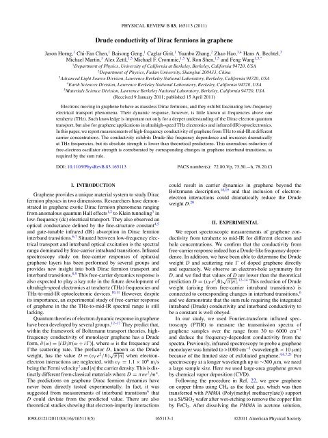
JASON HORNG et al. PHYSICAL REVIEW B 83, 165113 (2011)<br />
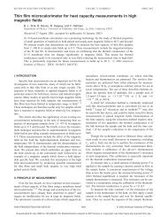
at V = 0 and a hole mobility around 2700 cm 2 /Vs.As<br />
-50 0<br />
(a)<br />
(b)<br />
5%. The sample had an <strong>in</strong>itial hole dop<strong>in</strong>g <strong>of</strong> 1.05 × 10 12 cm −2 electron dop<strong>in</strong>g. This electron-hole concentration dependence<br />
40<br />
g<br />
seen from Fig. 1(b), the dc <strong>conductivity</strong> for hole dop<strong>in</strong>g is<br />
30<br />
reasonably l<strong>in</strong>ear with |n|, and there is a large asymmetry<br />
between electron and hole <strong>conductivity</strong> at the same |n|. In<br />
20<br />
previous studies, conclusions have frequently been made on<br />
10<br />
carrier scatter<strong>in</strong>g from such dc <strong>conductivity</strong> data based on<br />
σ dc = D/πƔ and the assumption that D = (v F e 2 / ¯h) √ π|n|<br />
0<br />
holds exactly as theory predicts. 23–25 However, the validity <strong>of</strong><br />
50<br />
V g<br />
(V)<br />
100<br />
this approach has never been tested.<br />
5<br />
2E has two characteristic features: a large absorption <strong>in</strong>crease at<br />
F<br />
0<br />
lower wave numbers, which reaches over 15% at terahertz<br />
0 1500 3000 4500 6000<br />
frequencies for a <strong>graphene</strong> monolayer, and an absorption<br />
ω(cm -1 )<br />
reduction over a broad range <strong>of</strong> higher wave numbers. These<br />
(c)<br />
20<br />
(d)<br />
An <strong>in</strong>dependent determ<strong>in</strong>ation <strong>of</strong> D and Ɣ can be achieved<br />
through ac <strong>conductivity</strong> measurements us<strong>in</strong>g IR spectroscopy.<br />
15<br />
Figure 1(c) shows a difference IR absorption spectrum <strong>of</strong><br />
10<br />
hole-doped <strong>graphene</strong> (V g =−70 V) <strong>in</strong> reference to absorption<br />
at the CNP (V g = 14 V). This difference absorption spectrum<br />
features can be understood qualitatively from the gate-<strong>in</strong>duced<br />
FIG. 1. (Color onl<strong>in</strong>e) Properties <strong>of</strong> CVD-grown <strong>graphene</strong><br />
changes <strong>in</strong> <strong>in</strong>traband and <strong>in</strong>terband electronic transitions <strong>in</strong><br />
device. (a) Optical microscope image <strong>of</strong> CVD-grown <strong>graphene</strong><br />
<strong>graphene</strong> due to carrier dop<strong>in</strong>g [Fig. 1(d)]. Free-carrier <strong>conductivity</strong><br />
(from <strong>in</strong>traband transitions) <strong>in</strong>creases dramatically<br />
transferred to a SiO 2 /Si substrate. (b) Graphene dc <strong>conductivity</strong><br />
as a function <strong>of</strong> gate voltage. The <strong>conductivity</strong> m<strong>in</strong>imum at V g =<br />
with the hole dop<strong>in</strong>g. It peaks at zero frequency and gives rise<br />
14 V def<strong>in</strong>es the charge neutral po<strong>in</strong>t (CNP). (c) Gate-<strong>in</strong>duced change<br />
to a substantial absorption <strong>in</strong>crease at low wave numbers. At<br />
<strong>of</strong> ir transmittance T/T through <strong>graphene</strong> at V g =−70 V (hole<br />
doped) compared to transmittance at the CNP. The spectrum shows<br />
the same time, however, the <strong>in</strong>terband transitions up to energy<br />
an <strong>in</strong>crease <strong>of</strong> free-carrier absorption at low wave numbers and a 2E F [arrows <strong>in</strong> Fig. 1(d)] become forbidden due to empty<br />
reduction <strong>of</strong> <strong>in</strong>terband absorption at higher wave numbers. (d) An <strong>in</strong>itial states, lead<strong>in</strong>g to a reduction <strong>of</strong> absorption <strong>in</strong> the broad<br />
illustration <strong>of</strong> <strong>in</strong>traband (i.e., free-carrier absorption, dashed arrow) spectral range below 2E F [dashed l<strong>in</strong>e <strong>in</strong> Fig. 1(c)].<br />
and <strong>in</strong>terband (solid arrow) transitions <strong>in</strong> hole-doped <strong>graphene</strong>. The gate-<strong>in</strong>duced change <strong>of</strong> ac <strong>conductivity</strong> (referred to as<br />
Intraband absorption <strong>in</strong>creases with carrier dop<strong>in</strong>g, while <strong>in</strong>terband the CNP value), ˜σ = ˜σ − ˜σ CNP , can be obta<strong>in</strong>ed readily from<br />
transitions up to 2E F become forbidden due to empty <strong>in</strong>itial states, the difference IR absorption spectra (see auxiliary material).<br />
as observed <strong>in</strong> (c).<br />
Figures 2(a) and 2(b) show the real part <strong>of</strong> the ac <strong>conductivity</strong><br />
change σ ′ <strong>in</strong> the low-wave-number range (
DRUDE CONDUCTIVITY OF DIRAC FERMIONS IN GRAPHENE PHYSICAL REVIEW B 83, 165113 (2011)<br />
(a)<br />
Δσ' (e 2 /h)<br />
(c)<br />
Γ(cm -1 )<br />
(e)<br />
σ DC<br />
(e 2 /h)<br />
25<br />
20<br />
15<br />
10<br />
5<br />
0<br />
0 150 300 450<br />
ω(cm -1 )<br />
180<br />
150<br />
120<br />
90<br />
60<br />
Hole<br />
Electron<br />
30 regime regime<br />
0<br />
-100 -50 0 50<br />
V g<br />
-V cnp<br />
(V)<br />
40<br />
30<br />
20<br />
10<br />
Hole<br />
regime<br />
D/πΓ<br />
σ DC<br />
0<br />
-100 -50 0<br />
V g<br />
-V cnp<br />
(V)<br />
50<br />
V g<br />
-V cnp<br />
-80V<br />
-50V<br />
-20V<br />
0V<br />
(b)<br />
Δσ' (e 2 /h)<br />
(d)<br />
D (e 2 /h*1000cm -1 )<br />
25<br />
20<br />
15<br />
10<br />
5<br />
0<br />
0 150 300 450<br />
ω(cm -1 )<br />
15<br />
12<br />
9<br />
6<br />
3<br />
Hole<br />
regime<br />
Electron<br />
regime<br />
Theory<br />
Experiment<br />
Electron<br />
regime<br />
0<br />
-100 -50 0<br />
V g<br />
-V cnp<br />
(V)<br />
50<br />
V g<br />
-V cnp<br />
50V<br />
20V<br />
0V<br />
FIG. 2. (Color onl<strong>in</strong>e) Free-carrier responses <strong>in</strong> <strong>graphene</strong>. (a),(b)<br />
Gate-<strong>in</strong>duced change <strong>of</strong> ac <strong>conductivity</strong> σ ′ <strong>in</strong> hole- and electrondoped<br />
<strong>graphene</strong>, respectively, for 30
JASON HORNG et al. PHYSICAL REVIEW B 83, 165113 (2011)<br />
<strong>in</strong>terband absorption has also been observed previously for<br />
mechanically exfoliated <strong>graphene</strong>. 6 Based on the sum rule that<br />
we established experimentally, it <strong>in</strong>dicates that the anomalous<br />
<strong>Drude</strong> weight reduction is general for both exfoliated and CVD<br />
samples.<br />
This reduction <strong>of</strong> <strong>Drude</strong> weight cannot be easily understood.<br />
One theoretical study showed that electron-electron<br />
<strong>in</strong>teractions <strong>in</strong> <strong>graphene</strong> could lead to a reduced <strong>Drude</strong><br />
weight. 18 However, this theory predicted a much larger<br />
reduction <strong>of</strong> the <strong>Drude</strong> weight (over 80%) for <strong>graphene</strong><br />
on SiO 2 than what we have observed. It is also possible<br />
that a reduction <strong>of</strong> D is a consequence <strong>of</strong> defect-<strong>in</strong>duced<br />
electron or hole localization, which decreases the effective<br />
“free” electron or hole concentration. In addition, the electronimpurity<br />
<strong>in</strong>teractions may play a role and contribute to the<br />
observed electron-hole asymmetry. 19 Further experiments with<br />
higher-quality <strong>graphene</strong> will be required to p<strong>in</strong> down the<br />
underly<strong>in</strong>g mechanism for the <strong>Drude</strong> weight reduction.<br />
IV. SUMMARY<br />
Our <strong>in</strong>frared spectroscopy shows that the frequencydependent<br />
response <strong>of</strong> a <strong>Dirac</strong> fermion <strong>in</strong> <strong>graphene</strong> can be<br />
described by the <strong>Drude</strong> form, which becomes very strong<br />
at longer wavelengths. In the THz range (λ ∼ 300 μm),<br />
a gated <strong>graphene</strong> monolayer can absorb over 15% <strong>of</strong> the<br />
<strong>in</strong>cident radiation, suggest<strong>in</strong>g that <strong>graphene</strong> can potentially<br />
be a useful new THz material. More importantly, the <strong>in</strong>dependent<br />
determ<strong>in</strong>ation <strong>of</strong> <strong>Drude</strong> weight and scatter<strong>in</strong>g rate<br />
for the free carriers <strong>in</strong> <strong>graphene</strong> has allowed us to discover<br />
that the free-carrier <strong>Drude</strong> weight is significantly smaller than<br />
the predictions from Boltzmann transport theory, but the sum<br />
rule for <strong>in</strong>tegrated <strong>in</strong>traband and <strong>in</strong>terband oscillator strength<br />
is strictly obeyed.<br />
ACKNOWLEDGMENTS<br />
This work was supported by the US Department <strong>of</strong> Energy,<br />
Laboratory Directed Research and Development Program <strong>of</strong><br />
Lawrence Berkeley National Laboratory under Contract No.<br />
DE-AC02-05CH11231, the Office <strong>of</strong> Basic Energy Sciences<br />
under Contract No. DE-AC03-76SF0098 (Materials Science<br />
Division) and Contract No. DE-AC02-05CH11231 (Advanced<br />
Light Source), and ONR MURI Award No. N00014-09-1-<br />
1066.<br />
APPENDIX: CALCULATING THE AC CONDUCTIVITY<br />
The frequency-dependent <strong>conductivity</strong> change <strong>of</strong> <strong>graphene</strong><br />
˜σ at different gate voltages is obta<strong>in</strong>ed from the measured<br />
transmission spectra us<strong>in</strong>g a perturbation treatment, because<br />
a monolayer <strong>graphene</strong> only absorbs a small fraction <strong>of</strong> the<br />
light. With<strong>in</strong> this approximation, the complex ac <strong>conductivity</strong><br />
change is related to the difference transmission spectra by<br />
−T<br />
(ω) = 4π Re( ˜σ × L),<br />
T c (A1)<br />
where −T /T is the normalized transmission difference, L is<br />
the local field factor, and ˜σ is the gate-<strong>in</strong>duced <strong>conductivity</strong><br />
change <strong>in</strong> <strong>graphene</strong>.<br />
For suspended <strong>graphene</strong>, the local field factor is 1, and we<br />
obta<strong>in</strong> the well-known form <strong>of</strong> (−T /T )(ω) = (4π/c)σ ′ . 5<br />
In our device, the <strong>graphene</strong> is sitt<strong>in</strong>g on a SiO 2 /Si substrate<br />
and the local field factor L is uniquely def<strong>in</strong>ed by the refractive<br />
<strong>in</strong>dex <strong>of</strong> Si and SiO 2 , as well as the thickness <strong>of</strong> SiO 2 , and it can<br />
be determ<strong>in</strong>ed accurately without any adjust<strong>in</strong>g parameters.<br />
Specifically, L has the form<br />
e 2ikn gd<br />
L = 1 + r ag + t ag r gs t ga<br />
1 − e 2ikngd , (A2)<br />
r gs r ga<br />
where r ag ,r gs , and r ga are the Fresnel reflection coefficients<br />
at air-silica, silica-silicon, and silica-air <strong>in</strong>terferences, t ag and<br />
t ga are the correspond<strong>in</strong>g transmission coefficients, n g and d<br />
are the complex reflective <strong>in</strong>dex and thickness <strong>of</strong> the SiO 2<br />
layer, respectively, and k is the wave vector <strong>of</strong> the <strong>in</strong>cident<br />
light.<br />
The real and imag<strong>in</strong>ary parts <strong>of</strong> ac <strong>conductivity</strong>, σ ′ andσ ′′ ,<br />
are connected by the Kramers-Kronig (KK) relation<br />
σ ′′ (ω) = −2ω<br />
π<br />
∫ ∞<br />
0<br />
σ ′ (¯ω)d ¯ω<br />
¯ω 2 − ω 2 .<br />
(A3)<br />
Because the KK relation holds true for all the gate voltages,<br />
the gate-<strong>in</strong>duced <strong>conductivity</strong> change σ = σ ′ + iσ ′′ also<br />
satisfies the same KK relation. Mak<strong>in</strong>g use <strong>of</strong> Eq. (A1) and<br />
the KK relation, we obta<strong>in</strong> both the real and imag<strong>in</strong>ary parts<br />
<strong>of</strong> the gate-<strong>in</strong>duced ac <strong>conductivity</strong> from <strong>in</strong>frared transmission<br />
spectra.<br />
The gate-<strong>in</strong>duced <strong>in</strong>frared absorption from the p-doped Si<br />
substrate is negligible. The real part <strong>of</strong> hole ac <strong>conductivity</strong><br />
<strong>in</strong> silicon is described by σ ′ = (ne 2 /m h )[Ɣ/(Ɣ 2 + ω 2 )]. For<br />
the same carrier density, it is more than one order <strong>of</strong> magnitude<br />
smaller than <strong>graphene</strong> <strong>conductivity</strong> across the experimental<br />
spectral range (30
DRUDE CONDUCTIVITY OF DIRAC FERMIONS IN GRAPHENE PHYSICAL REVIEW B 83, 165113 (2011)<br />
8 J. M. Dawlaty, S. Shivaraman, M. Chandrashekhar, F. Rana, and<br />
M. G. Spencer, Appl. Phys. Lett. 92, 042116 (2008).<br />
9 H. Choi, F. Borondics, D. A. Siegel, S. Y. Zhou, M. C. Mart<strong>in</strong>,<br />
A. Lanzara, and R. A. Ka<strong>in</strong>dl, Appl. Phys. Lett. 94, 172102 (2009).<br />
10 V. Ryzhii, A. Satou, and T. Otsuji, J. Appl. Phys. 101, 024509<br />
(2007).<br />
11 F. Rana, IEEE Trans. Nanotechnol. 7, 91 (2008).<br />
12 T. Ando, J. Phys. Soc. Jpn. 75, 074716 (2006).<br />
13 E. H. Hwang, S. Adam, and S. Das Sarma, Phys.Rev.Lett.98,<br />
186806 (2007).<br />
14 K. Nomura and A. H. MacDonald, Phys. Rev. Lett. 98, 076602<br />
(2007).<br />
15 N. M. R. Peres, J. M. B. L. dos Santos, and T. Stauber, Phys. Rev.<br />
B 76, 073412 (2007).<br />
16 T. Stauber, N. M. R. Peres, and F. Gu<strong>in</strong>ea, Phys. Rev. B 76, 205423<br />
(2007).<br />
17 A. H. Castro Neto, F. Gu<strong>in</strong>ea, N. M. R. Peres, K. S. Novoselov, and<br />
A. K. Geim, Rev. Mod. Phys. 81, 109 (2009).<br />
18 M. M. Fogler, D. S. Novikov, and B. I. Shklovskii, Phys.Rev.B<br />
76, 233402 (2007).<br />
19 A. V. Shytov, M. I. Katsnelson, and L. S. Levitov, Phys. Rev. Lett.<br />
99, 246802 (2007).<br />
20 M. Pol<strong>in</strong>i, A. H. MacDonald, and G. Vignale, e-pr<strong>in</strong>t<br />
arXiv:0901.4528.<br />
21 Y. B. Zhang, T. T. Tang, C. Girit, Z. Hao, M. C. Mart<strong>in</strong>, A. Zettl,<br />
M. F. Crommie, Y. R. Shen, and F. Wang, Nature (London) 459,<br />
820 (2009).<br />
22 X.S.Li,W.W.Cai,J.H.An,S.Y.Kim,J.Nah,D.X.Yang,<br />
R. P<strong>in</strong>er, A. Velamakanni, I. Jung, E. Tutuc, S. K. Banerjee,<br />
L. Colombo, and R. S. Ru<strong>of</strong>f, Science 324, 1312 (2009).<br />
23 Y. W. Tan, Y. Zhang, K. Bolot<strong>in</strong>, Y. Zhao, S. Adam, E. H. Hwang,<br />
S. Das Sarma, H. L. Stormer, and P. Kim, Phys.Rev.Lett.99,<br />
246803 (2007).<br />
24 J. H. Chen, C. Jang, S. Adam, M. S. Fuhrer, E. D. Williams, and<br />
M. Ishigami, Nat. Phys. 4, 377 (2008).<br />
25 X. Hong, K. Zou, and J. Zhu, Phys.Rev.B80, 241415 (2009).<br />
26 N. M. R. Peres, T. Stauber, and A. H. C. Neto, Europhys. Lett. 86,<br />
38002 (2009).<br />
27 S. Adam, E. H. Hwang, V. M. Galitski, and S. Das Sarma, Proc.<br />
Natl. Acad. Sci. USA 104, 18392 (2007).<br />
28 T. Ando, Y. S. Zheng, and H. Suzuura, J. Phys. Soc. Jpn. 71, 1318<br />
(2002).<br />
29 N. M. R. Peres, F. Gu<strong>in</strong>ea, and A. H. C. Neto, Phys. Rev. B 73,<br />
125411 (2006).<br />
30 V. P. Gusyn<strong>in</strong> and S. G. Sharapov, Phys. Rev. B 73, 245411<br />
(2006).<br />
31 M. Vanexter and D. Grischkowsky, Phys. Rev. B 41, 12140<br />
(1990).<br />
165113-5