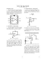
BJT and CE Amplifier - UC Davis
BJT and CE Amplifier - UC Davis
BJT and CE Amplifier - UC Davis

Create successful ePaper yourself
Turn your PDF publications into a flip-book with our unique Google optimized e-Paper software.
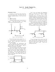
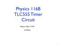
2. COMMON EMITTER AMPLIFIER<br />
In this section, you will build <strong>and</strong> analyze a<br />
common emitter amplifier, a popular transistor<br />
amplifier circuit. Build the amplifier as shown<br />
in figure 2 but don't connect the AC source yet.<br />
Just leave v in<br />
floating for now.<br />
First, find the bias conditions of the<br />
transistor. That is, find the voltages <strong>and</strong> currents<br />
in the circuit with no input signal. This is also<br />
called the "quiescent point", the "operating<br />
point", or the "DC" conditions for the circuit.<br />
To do this, measure V B<br />
, V E<br />
, <strong>and</strong> V C<br />
, use Ohm's<br />
law to calculate I E<br />
<strong>and</strong> I C<br />
, calculate IB<br />
= IC<br />
β<br />
using the β you found in section 1, <strong>and</strong> calculate<br />
V BE<br />
. The purpose of the resistors in the middle<br />
of the circuit, the "bias resistors", is to keep the<br />
transistor in its active region all the time. Is the<br />
transistor in its active region now?<br />
Now connect the function generator to v in<br />
<strong>and</strong> use a 1V peak-to-peak 10kHz sine wave as<br />
the input signal. Monitor v in<br />
<strong>and</strong> v out<br />
simultaneously with the oscilloscope <strong>and</strong> sketch<br />
them on the same set of axes. Measure the gain<br />
of this amplifier. Compare it to the calculated<br />
gain, RC<br />
RE . Note the phase difference from<br />
input to output. Most amplifiers invert the<br />
signals they amplify.<br />
Explore the behavior of the amplifier a little<br />
more by using different waveforms, frequencies,<br />
<strong>and</strong> amplitudes for v in<br />
. The output of an ideal<br />
amplifier should always look just like the input<br />
multiplied by the gain. However, real amplifiers<br />
only work correctly over a limited range of<br />
output voltages<br />
+15V<br />
<strong>and</strong> frequencies.<br />
Determining these<br />
ranges is an<br />
important part of<br />
116A's classroom<br />
100k Ω<br />
work. See if you<br />
can determine<br />
approximately the<br />
minimum <strong>and</strong> v<br />
in<br />
maximum<br />
frequencies for 0.1 µ F<br />
which the gain is<br />
constant. Also,<br />
see if you can<br />
determine the<br />
range of<br />
10k Ω<br />
acceptable output ~<br />
voltages. Try to<br />
guess what causes<br />
each of these<br />
limits.<br />
4.7 µ F<br />
(add later)<br />
For your report, include your DC<br />
measurements <strong>and</strong> calculations with a brief<br />
discussion of whether the transistor is in its<br />
active region, a sketch of v in<br />
<strong>and</strong> v out<br />
, a<br />
comparison of your measured <strong>and</strong> calculated gain,<br />
<strong>and</strong> some approximate frequency <strong>and</strong> voltage<br />
limits with guesses as to their causes.<br />
Optional: See how the gain changes when<br />
you add the 4.7µF capacitor (drawn with dashed<br />
lines). Can you explain this?<br />
V B<br />
I B<br />
I C<br />
I E<br />
+15V<br />
R = 10k Ω<br />
C<br />
V E<br />
V <strong>and</strong> v<br />
C out<br />
R = 1kΩ<br />
E<br />
Figure 2: A common emitter amplifier.<br />
9