Lab 13: Inside Digital ICs - UC Davis
Lab 13: Inside Digital ICs - UC Davis
Lab 13: Inside Digital ICs - UC Davis

Create successful ePaper yourself
Turn your PDF publications into a flip-book with our unique Google optimized e-Paper software.
<strong>Lab</strong> <strong>13</strong>: <strong>Inside</strong> <strong>Digital</strong> <strong>ICs</strong><br />
U.C. <strong>Davis</strong> Physics 116B<br />
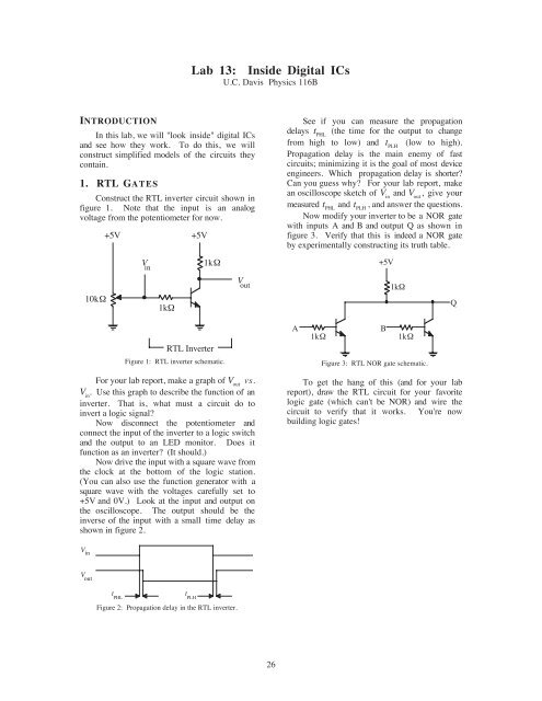
INTROD<strong>UC</strong>TION<br />
In this lab, we will "look inside" digital <strong>ICs</strong><br />
and see how they work. To do this, we will<br />
construct simplified models of the circuits they<br />
contain.<br />
1. RTL GATES<br />
Construct the RTL inverter circuit shown in<br />
figure 1. Note that the input is an analog<br />
voltage from the potentiometer for now.<br />
+5V<br />
+5V<br />
See if you can measure the propagation<br />
delays t PHL<br />
(the time for the output to change<br />
from high to low) and t PLH<br />
(low to high).<br />
Propagation delay is the main enemy of fast<br />
circuits; minimizing it is the goal of most device<br />
engineers. Which propagation delay is shorter?<br />
Can you guess why? For your lab report, make<br />
an oscilloscope sketch of V in<br />
and V out<br />
, give your<br />
measured t PHL<br />
and t PLH<br />
, and answer the questions.<br />
Now modify your inverter to be a NOR gate<br />
with inputs A and B and output Q as shown in<br />
figure 3. Verify that this is indeed a NOR gate<br />
by experimentally constructing its truth table.<br />
10kΩ<br />
V<br />
in<br />
1kΩ<br />
1kΩ<br />
V<br />
out<br />
+5V<br />
1kΩ<br />
Q<br />
RTL Inverter<br />
Figure 1: RTL inverter schematic.<br />
A<br />
B<br />
1kΩ<br />
1kΩ<br />
Figure 3: RTL NOR gate schematic.<br />
For your lab report, make a graph of V out<br />
vs.<br />
V in<br />
. Use this graph to describe the function of an<br />
inverter. That is, what must a circuit do to<br />
invert a logic signal?<br />
Now disconnect the potentiometer and<br />
connect the input of the inverter to a logic switch<br />
and the output to an LED monitor. Does it<br />
function as an inverter? (It should.)<br />
Now drive the input with a square wave from<br />
the clock at the bottom of the logic station.<br />
(You can also use the function generator with a<br />
square wave with the voltages carefully set to<br />
+5V and 0V.) Look at the input and output on<br />
the oscilloscope. The output should be the<br />
inverse of the input with a small time delay as<br />
shown in figure 2.<br />
To get the hang of this (and for your lab<br />
report), draw the RTL circuit for your favorite<br />
logic gate (which can't be NOR) and wire the<br />
circuit to verify that it works. You're now<br />
building logic gates!<br />
Vin<br />
V<br />
out<br />
t<br />
PHL<br />
t<br />
PLH<br />
Figure 2: Propagation delay in the RTL inverter.<br />
26
2. STEP-BY-STEP D FLIP FLOP<br />
You will now construct a D flip flop (a<br />
memory circuit) in several steps.<br />
First, construct the S-R (set-reset) latch<br />
shown in figure 4. Determine the truth table for<br />
this circuit and explain why Q can be either 1 or<br />
0 when A and B are both 1. Draw a timing<br />
diagram to illustrate how this circuit works as a<br />
memory device.<br />
A<br />
B<br />
Figure 4: S-R latch.<br />
Now modify the S-R latch to have a gated<br />
data input as shown in figure 5. This is the<br />
"transparent latch" circuit. Construct a truth<br />
table for this circuit and explain its operation<br />
using a timing diagram as you did for the S-R<br />
latch.<br />
D<br />
Store<br />
Figure 5: S-R latch with gated data input.<br />
Q<br />
Q<br />
D<br />
Q<br />
Clk<br />
Figure 7: Toggle flip flop circuit.<br />
Congratulations. You have now made all<br />
the basic building blocks you need to construct a<br />
computer or almost any other piece of digital<br />
equipment. In the next weeks, we will use<br />
already-built versions of these same circuits to<br />
construct ever more useful things.<br />
3. OPEN-COLLECTOR OUTPUTS<br />
IC's with "open collector outputs" still use<br />
the single transistor output of the RTL gate<br />
(without the pullup resistor). The outputs of the<br />
these gates can be wired together to make a gate<br />
like the RTL NOR. This is called "wire-<br />
ORing". (Never wire together the outputs of a<br />
normal IC!) Construct the circuit of figure 8.<br />
For your lab report, give the complete truth table<br />
and logic diagram for this circuit. For the logic<br />
diagram, you will need to determine what type of<br />
gate the wire-ORed outputs act as. Note that this<br />
technique can be used to change voltage levels;<br />
the +5V can be replaced by +15V, for example.<br />
+5V<br />
7403, open-collector outputs<br />
10kΩ<br />
Now, add the rather crude edge trigger shown<br />
in figure 6 to your transparent latch. The<br />
complete circuit you now have should function<br />
like a D flip flop. Construct a truth table for<br />
this circuit and draw a timing diagram to<br />
illustrate how it works.<br />
Clk<br />
to<br />
"Store"<br />
above<br />
Figure 6: Edge trigger for D flip flop.<br />
The entire D flip flop is usually represented<br />
by a box as used in figure 7. Use your D flip<br />
flop to construct the circuit shown in figure 7.<br />
This is a toggle circuit; each time the clock<br />
pulses, the output will toggle from 0 to 1 and<br />
then from 1 to 0. Draw a timing diagram to<br />
illustrate how this works.<br />
A<br />
B<br />
C<br />
D<br />
*<br />
Note: never short together<br />
the outputs of most <strong>ICs</strong>.<br />
*<br />
Only open-collector and<br />
tri-state outputs should be<br />
used this way.<br />
Figure 8: Wire-OR demonstration circuit.<br />
Q<br />
27