JFET VHF Amplifier MPF102
JFET VHF Amplifier MPF102
JFET VHF Amplifier MPF102

Create successful ePaper yourself
Turn your PDF publications into a flip-book with our unique Google optimized e-Paper software.
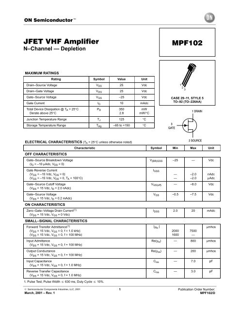
N–Channel — Depletion<br />
<br />
MAXIMUM RATINGS<br />
Rating Symbol Value Unit<br />
Drain–Source Voltage V DS 25 Vdc<br />
Drain–Gate Voltage V DG 25 Vdc<br />
Gate–Source Voltage V GS –25 Vdc<br />
Gate Current I G 10 mAdc<br />
Total Device Dissipation @ T A = 25°C<br />
Derate above 25°C<br />
P D 350<br />
2.8<br />
mW<br />
mW/°C<br />
Junction Temperature Range T J 125 °C<br />
Storage Temperature Range T stg –65 to +150 °C<br />
CASE 29–11, STYLE 5<br />
TO–92 (TO–226AA)<br />
<br />
<br />
1<br />
2<br />
3<br />
<br />
ELECTRICAL CHARACTERISTICS (T A = 25°C unless otherwise noted)<br />
Characteristic Symbol Min<br />
<br />
Max Unit<br />
OFF CHARACTERISTICS<br />
Gate–Source Breakdown Voltage<br />
(I G = –10 µAdc, V DS = 0)<br />
V (BR)GSS –25 — Vdc<br />
Gate Reverse Current<br />
(V GS = –15 Vdc, V DS = 0)<br />
(V GS = –15 Vdc, V DS = 0, T A = 100°C)<br />
Gate–Source Cutoff Voltage<br />
(V DS = 15 Vdc, I D = 2.0 nAdc)<br />
Gate–Source Voltage<br />
(V DS = 15 Vdc, I D = 0.2 mAdc)<br />
ON CHARACTERISTICS<br />
Zero–Gate–Voltage Drain Current (1)<br />
(V DS = 15 Vdc, V GS = 0 Vdc)<br />
SMALL–SIGNAL CHARACTERISTICS<br />
Forward Transfer Admittance (1)<br />
(V DS = 15 Vdc, V GS = 0, f = 1.0 kHz)<br />
(V DS = 15 Vdc, V GS = 0, f = 100 MHz)<br />
Input Admittance<br />
(V DS = 15 Vdc, V GS = 0, f = 100 MHz)<br />
Output Conductance<br />
(V DS = 15 Vdc, V GS = 0, f = 100 MHz)<br />
Input Capacitance<br />
(V DS = 15 Vdc, V GS = 0, f = 1.0 MHz)<br />
Reverse Transfer Capacitance<br />
(V DS = 15 Vdc, V GS = 0, f = 1.0 MHz)<br />
I GSS<br />
—<br />
—<br />
–2.0<br />
–2.0<br />
nAdc<br />
µAdc<br />
V GS(off) — –8.0 Vdc<br />
V GS –0.5 –7.5 Vdc<br />
I DSS 2.0 20 mAdc<br />
⎪y fs ⎟<br />
2000<br />
1600<br />
7500<br />
—<br />
mhos<br />
Re(y is ) — 800 mhos<br />
Re(y os ) — 200 mhos<br />
C iss — 7.0 pF<br />
C rss — 3.0 pF<br />
1. Pulse Test; Pulse Width 630 ms, Duty Cycle 10%.<br />
© Semiconductor Components Industries, LLC, 2001<br />
March, 2001 – Rev. 1<br />
1 Publication Order Number:<br />
<strong>MPF102</strong>/D
<strong>MPF102</strong><br />
POWER GAIN<br />
<br />
<br />
<br />
<br />
<br />
<br />
<br />
<br />
°<br />
<br />
<br />
<br />
<br />
<br />
Figure 1. Effects of Drain Current<br />
<br />
Ω<br />
<br />
<br />
Adjust V GS for<br />
I D = 50 mA<br />
V GS < 0 Volts<br />
<br />
<br />
′<br />
<br />
<br />
<br />
<br />
<br />
NOTE:<br />
<br />
<br />
<br />
<br />
<br />
<br />
<br />
<br />
<br />
<br />
Ω<br />
<br />
The noise source is a hot–cold body<br />
(AIL type 70 or equivalent) with a<br />
test receiver (AIL type 136 or equivalent).<br />
Reference<br />
VALUE<br />
Designation 100 MHz 400 MHz<br />
C1 7.0 pF 1.8 pF<br />
C2 1000 pF 17 pF<br />
C3 3.0 pF 1.0 pF<br />
C4 1–12 pF 0.8–8.0 pF<br />
C5 1–12 pF 0.8–8.0 pF<br />
C6 0.0015 µF 0.001 µF<br />
C7 0.0015 µF 0.001 µF<br />
L1 3.0 µH* 0.2 µH**<br />
L2 0.15 µH* 0.03 µH**<br />
L3 0.14 µH* 0.022 µH**<br />
*L1 17 turns, (approx. — depends upon circuit layout) AWG #28<br />
enameled copper wire, close wound on 9/32″ ceramic coil<br />
form. Tuning provided by a powdered iron slug.<br />
*L2 4–1/2 turns, AWG #18 enameled copper wire, 5/16″ long,<br />
3/8″ I.D. (AIR CORE).<br />
*L3 3–1/2 turns, AWG #18 enameled copper wire, 1/4″ long,<br />
3/8″ I.D. (AIR CORE).<br />
Figure 2. 100 MHz and 400 MHz Neutralized Test Circuit<br />
**L1 6 turns, (approx. — depends upon circuit layout) AWG #24<br />
enameled copper wire, close wound on 7/32″ ceramic coil<br />
form. Tuning provided by an aluminum slug.<br />
**L2 1 turn, AWG #16 enameled copper wire, 3/8″ I.D.<br />
(AIR CORE).<br />
**L3 1/2 turn, AWG #16 enameled copper wire, 1/4″ I.D.<br />
(AIR CORE).<br />
http://onsemi.com<br />
2
<strong>MPF102</strong><br />
NOISE FIGURE<br />
(T channel = 25°C)<br />
<br />
<br />
<br />
<br />
<br />
<br />
<br />
<br />
<br />
<br />
<br />
<br />
<br />
<br />
<br />
<br />
<br />
<br />
<br />
<br />
<br />
<br />
Figure 3. Effects of Drain–Source Voltage<br />
<br />
<br />
<br />
Figure 4. Effects of Drain Current<br />
<br />
<br />
<br />
<br />
<br />
<br />
<br />
<br />
<br />
<br />
<br />
<br />
INTERMODULATION CHARACTERISTICS<br />
<br />
<br />
<br />
<br />
<br />
<br />
<br />
<br />
<br />
<br />
<br />
<br />
<br />
Figure 5. Third Order Intermodulation Distortion<br />
http://onsemi.com<br />
3
<strong>MPF102</strong><br />
COMMON SOURCE CHARACTERISTICS<br />
ADMITTANCE PARAMETERS<br />
(V DS = 15 Vdc, T channel = 25°C)<br />
<br />
<br />
<br />
<br />
<br />
<br />
<br />
<br />
<br />
<br />
<br />
<br />
<br />
<br />
<br />
<br />
<br />
<br />
<br />
<br />
<br />
<br />
<br />
<br />
<br />
<br />
<br />
<br />
<br />
<br />
<br />
<br />
<br />
<br />
<br />
<br />
<br />
<br />
Figure 6. Input Admittance (y is ) Figure 7. Reverse Transfer Admittance (y rs )<br />
<br />
<br />
<br />
<br />
<br />
<br />
<br />
<br />
<br />
<br />
<br />
<br />
<br />
<br />
<br />
<br />
<br />
<br />
<br />
<br />
<br />
<br />
<br />
<br />
<br />
<br />
<br />
<br />
<br />
<br />
<br />
<br />
<br />
<br />
<br />
Figure 8. Forward Transadmittance (y fs ) Figure 9. Output Admittance (y os )<br />
http://onsemi.com<br />
4
<strong>MPF102</strong><br />
COMMON SOURCE CHARACTERISTICS<br />
S–PARAMETERS<br />
(V DS = 15 Vdc, T channel = 25°C, Data Points in MHz)<br />
°<br />
°<br />
°<br />
° ° ° °<br />
°<br />
°<br />
°<br />
° ° ° °<br />
°<br />
°<br />
°<br />
°<br />
°<br />
°<br />
<br />
<br />
<br />
<br />
<br />
<br />
<br />
<br />
<br />
<br />
<br />
<br />
<br />
<br />
<br />
<br />
<br />
<br />
<br />
<br />
<br />
°<br />
°<br />
°<br />
°<br />
°<br />
°<br />
°<br />
°<br />
°<br />
°<br />
°<br />
°<br />
<br />
<br />
<br />
<br />
<br />
<br />
<br />
<br />
<br />
<br />
<br />
<br />
<br />
<br />
<br />
°<br />
°<br />
°<br />
°<br />
°<br />
°<br />
°<br />
°<br />
°<br />
°<br />
°<br />
°<br />
°<br />
°<br />
°<br />
°<br />
°<br />
°<br />
°<br />
°<br />
°<br />
°<br />
°<br />
°<br />
°<br />
°<br />
°<br />
°<br />
°<br />
° ° ° °<br />
°<br />
°<br />
°<br />
° ° ° °<br />
Figure 10. S 11s<br />
Figure 11. S 12s<br />
°<br />
°<br />
°<br />
°<br />
°<br />
°<br />
° ° ° °<br />
<br />
<br />
°<br />
°<br />
°<br />
°<br />
°<br />
°<br />
°<br />
°<br />
°<br />
° ° ° °<br />
<br />
<br />
<br />
<br />
<br />
<br />
<br />
<br />
<br />
<br />
<br />
<br />
<br />
<br />
<br />
<br />
<br />
°<br />
°<br />
°<br />
°<br />
°<br />
°<br />
°<br />
°<br />
°<br />
<br />
<br />
<br />
<br />
<br />
<br />
<br />
<br />
<br />
<br />
<br />
<br />
<br />
<br />
<br />
<br />
<br />
<br />
<br />
<br />
<br />
<br />
°<br />
°<br />
°<br />
°<br />
°<br />
°<br />
°<br />
°<br />
°<br />
°<br />
°<br />
°<br />
<br />
<br />
°<br />
°<br />
°<br />
°<br />
°<br />
°<br />
°<br />
<br />
°<br />
°<br />
°<br />
°<br />
°<br />
°<br />
°<br />
°<br />
°<br />
°<br />
° ° ° °<br />
°<br />
°<br />
°<br />
° ° ° °<br />
Fi S Fi S<br />
http://onsemi.com<br />
5
<strong>MPF102</strong><br />
COMMON GATE CHARACTERISTICS<br />
ADMITTANCE PARAMETERS<br />
(V DG = 15 Vdc, T channel = 25°C)<br />
<br />
<br />
<br />
<br />
<br />
<br />
<br />
<br />
<br />
<br />
<br />
<br />
<br />
<br />
<br />
<br />
<br />
<br />
<br />
<br />
<br />
<br />
<br />
<br />
<br />
<br />
<br />
<br />
<br />
<br />
<br />
<br />
<br />
<br />
<br />
<br />
<br />
<br />
<br />
Figure 14. Input Admittance (y ig ) Figure 15. Reverse Transfer Admittance (y rg )<br />
<br />
<br />
<br />
<br />
<br />
<br />
<br />
<br />
<br />
<br />
<br />
<br />
<br />
<br />
<br />
<br />
<br />
<br />
<br />
<br />
<br />
<br />
<br />
<br />
<br />
<br />
<br />
<br />
<br />
<br />
<br />
<br />
<br />
<br />
<br />
<br />
Figure 16. Forward Transfer Admittance (y fg ) Figure 17. Output Admittance (y og )<br />
http://onsemi.com<br />
6
<strong>MPF102</strong><br />
COMMON GATE CHARACTERISTICS<br />
S–PARAMETERS<br />
(V DS = 15 Vdc, T channel = 25°C, Data Points in MHz)<br />
°<br />
°<br />
°<br />
° ° ° °<br />
°<br />
°<br />
°<br />
° ° ° °<br />
°<br />
<br />
<br />
°<br />
°<br />
<br />
°<br />
°<br />
°<br />
°<br />
°<br />
°<br />
°<br />
°<br />
°<br />
°<br />
<br />
<br />
<br />
<br />
<br />
<br />
<br />
<br />
<br />
<br />
<br />
<br />
<br />
<br />
<br />
<br />
<br />
<br />
<br />
<br />
°<br />
°<br />
°<br />
°<br />
°<br />
°<br />
°<br />
°<br />
°<br />
°<br />
°<br />
°<br />
°<br />
°<br />
°<br />
°<br />
°<br />
°<br />
<br />
<br />
<br />
<br />
<br />
<br />
<br />
<br />
<br />
<br />
<br />
<br />
<br />
<br />
<br />
<br />
<br />
<br />
<br />
°<br />
°<br />
°<br />
°<br />
°<br />
°<br />
°<br />
°<br />
°<br />
°<br />
°<br />
°<br />
<br />
°<br />
°<br />
°<br />
°<br />
° ° ° °<br />
°<br />
°<br />
°<br />
° ° ° °<br />
Figure 18. S 11g<br />
Figure 19. S 12g<br />
°<br />
°<br />
°<br />
°<br />
°<br />
°<br />
°<br />
<br />
° ° ° °<br />
° ° ° ° ° ° °<br />
<br />
° °<br />
<br />
°<br />
<br />
°<br />
<br />
<br />
<br />
° °<br />
<br />
<br />
<br />
<br />
<br />
<br />
<br />
<br />
<br />
<br />
<br />
<br />
<br />
° °<br />
°<br />
°<br />
°<br />
°<br />
°<br />
°<br />
°<br />
<br />
<br />
<br />
°<br />
°<br />
°<br />
°<br />
°<br />
°<br />
<br />
°<br />
°<br />
°<br />
°<br />
°<br />
°<br />
°<br />
°<br />
°<br />
°<br />
°<br />
°<br />
°<br />
°<br />
°<br />
°<br />
°<br />
°<br />
°<br />
°<br />
°<br />
°<br />
° ° ° °<br />
°<br />
°<br />
°<br />
° ° ° °<br />
http://onsemi.com<br />
7
<strong>MPF102</strong><br />
PACKAGE DIMENSIONS<br />
TO–92 (TO–226AB)<br />
CASE 29–11<br />
ISSUE AL<br />
A<br />
B<br />
<br />
<br />
<br />
<br />
R<br />
<br />
<br />
P<br />
<br />
<br />
L<br />
<br />
<br />
K<br />
<br />
<br />
<br />
<br />
X X<br />
D<br />
<br />
<br />
G<br />
<br />
H<br />
J<br />
<br />
<br />
<br />
V<br />
C<br />
<br />
N<br />
<br />
SECTION X–X<br />
<br />
<br />
N<br />
<br />
<br />
<br />
<br />
ON Semiconductor and are trademarks of Semiconductor Components Industries, LLC (SCILLC). SCILLC reserves the right to make changes<br />
without further notice to any products herein. SCILLC makes no warranty, representation or guarantee regarding the suitability of its products for any particular<br />
purpose, nor does SCILLC assume any liability arising out of the application or use of any product or circuit, and specifically disclaims any and all liability,<br />
including without limitation special, consequential or incidental damages. “Typical” parameters which may be provided in SCILLC data sheets and/or<br />
specifications can and do vary in different applications and actual performance may vary over time. All operating parameters, including “Typicals” must be<br />
validated for each customer application by customer’s technical experts. SCILLC does not convey any license under its patent rights nor the rights of others.<br />
SCILLC products are not designed, intended, or authorized for use as components in systems intended for surgical implant into the body, or other applications<br />
intended to support or sustain life, or for any other application in which the failure of the SCILLC product could create a situation where personal injury or<br />
death may occur. Should Buyer purchase or use SCILLC products for any such unintended or unauthorized application, Buyer shall indemnify and hold<br />
SCILLC and its officers, employees, subsidiaries, affiliates, and distributors harmless against all claims, costs, damages, and expenses, and reasonable<br />
attorney fees arising out of, directly or indirectly, any claim of personal injury or death associated with such unintended or unauthorized use, even if such claim<br />
alleges that SCILLC was negligent regarding the design or manufacture of the part. SCILLC is an Equal Opportunity/Affirmative Action Employer.<br />
PUBLICATION ORDERING INFORMATION<br />
NORTH AMERICA Literature Fulfillment:<br />
Literature Distribution Center for ON Semiconductor<br />
P.O. Box 5163, Denver, Colorado 80217 USA<br />
Phone: 303–675–2175 or 800–344–3860 Toll Free USA/Canada<br />
Fax: 303–675–2176 or 800–344–3867 Toll Free USA/Canada<br />
Email: ONlit@hibbertco.com<br />
Fax Response Line: 303–675–2167 or 800–344–3810 Toll Free USA/Canada<br />
N. American Technical Support: 800–282–9855 Toll Free USA/Canada<br />
EUROPE: LDC for ON Semiconductor – European Support<br />
German Phone: (+1) 303–308–7140 (Mon–Fri 2:30pm to 7:00pm CET)<br />
Email: ONlit–german@hibbertco.com<br />
French Phone: (+1) 303–308–7141 (Mon–Fri 2:00pm to 7:00pm CET)<br />
Email: ONlit–french@hibbertco.com<br />
English Phone: (+1) 303–308–7142 (Mon–Fri 12:00pm to 5:00pm GMT)<br />
Email: ONlit@hibbertco.com<br />
EUROPEAN TOLL–FREE ACCESS*: 00–800–4422–3781<br />
*Available from Germany, France, Italy, UK, Ireland<br />
CENTRAL/SOUTH AMERICA:<br />
Spanish Phone: 303–308–7143 (Mon–Fri 8:00am to 5:00pm MST)<br />
Email: ONlit–spanish@hibbertco.com<br />
Toll–Free from Mexico: Dial 01–800–288–2872 for Access –<br />
then Dial 866–297–9322<br />
ASIA/PACIFIC: LDC for ON Semiconductor – Asia Support<br />
Phone: 1–303–675–2121 (Tue–Fri 9:00am to 1:00pm, Hong Kong Time)<br />
Toll Free from Hong Kong & Singapore:<br />
001–800–4422–3781<br />
Email: ONlit–asia@hibbertco.com<br />
JAPAN: ON Semiconductor, Japan Customer Focus Center<br />
4–32–1 Nishi–Gotanda, Shinagawa–ku, Tokyo, Japan 141–0031<br />
Phone: 81–3–5740–2700<br />
Email: r14525@onsemi.com<br />
ON Semiconductor Website: http://onsemi.com<br />
For additional information, please contact your local<br />
Sales Representative.<br />
http://onsemi.com<br />
8<br />
<strong>MPF102</strong>/D