Smart Highside Power Switch
Smart Highside Power Switch
Smart Highside Power Switch

Create successful ePaper yourself
Turn your PDF publications into a flip-book with our unique Google optimized e-Paper software.
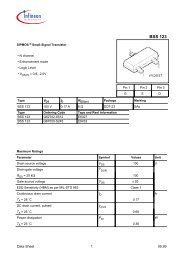
Pin Symbol Function<br />
1 GND - Logic ground<br />
BTS 410 D2<br />
2 IN I Input, activates the power switch in case of logical high signal<br />
3 Vbb + Positive power supply voltage,<br />
the tab is shorted to this pin<br />
4 ST S Diagnostic feedback, low on failure<br />
5 OUT<br />
(Load, L)<br />
O Output to the load<br />
Maximum Ratings at Tj = 25 °C unless otherwise specified<br />
Parameter Symbol Values Unit<br />
Supply voltage (overvoltage protection see page 3) V bb 65 V<br />
Load dump protection 2) V LoadDump = U A + V s , U A = 13.5 V V<br />
4) Load dump 100 V<br />
R I<br />
3)<br />
= 2 Ω, R L = 6.6 Ω, t d = 400 ms, IN= low or high<br />
Load current (Short circuit current, see page 4) I L self-limited A<br />
Operating temperature range<br />
T j<br />
-40 ...+150 °C<br />
Storage temperature range<br />
T stg -55 ...+150<br />
<strong>Power</strong> dissipation (DC), T C ≤ 25 °C P tot 50 W<br />
Inductive load switch-off energy dissipation, single pulse<br />
V bb = 12V, T j,start = 150°C, T C = 150°C const.<br />
I L = 1.8 A, Z L = 2.3 H, 0 Ω: E AS 4.5 J<br />
Electrostatic discharge capability (ESD)<br />
(Human Body Model)<br />
IN:<br />
all other pins:<br />
V ESD 1<br />
2<br />
kV<br />
acc. MIL-STD883D, method 3015.7 and ESD assn. std. S5.1-1993<br />
Input voltage (DC) V IN -0.5 ... +6 V<br />
Current through input pin (DC)<br />
I IN<br />
±5.0 mA<br />
Current through status pin (DC)<br />
I ST ±5.0<br />
see internal circuit diagrams page 6<br />
Thermal Characteristics<br />
--<br />
Parameter and Conditions Symbol Values Unit<br />
min typ max<br />
Thermal resistance<br />
chip - case: R thJC<br />
-- 2.5 K/W<br />
junction - ambient (free air): R thJA -- -- 75<br />
SMD version, device on PCB 5) : -- 35 --<br />
2) Supply voltages higher than V bb(AZ) require an external current limit for the GND and status pins, e.g. with a<br />
150 Ω resistor in the GND connection and a 15 kΩ resistor in series with the status pin. A resistor for the<br />
protection of the input is integrated.<br />
3) R I = internal resistance of the load dump test pulse generator<br />
4) V Load dump is setup without the DUT connected to the generator per ISO 7637-1 and DIN 40839<br />
5) Device on 50mm*50mm*1.5mm epoxy PCB FR4 with 6cm 2 (one layer, 70µm thick) copper area for V bb<br />
connection. PCB is vertical without blown air.<br />
Semiconductor Group 2