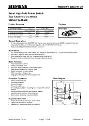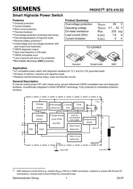
Smart Highside Power Switch
Smart Highside Power Switch
Smart Highside Power Switch

You also want an ePaper? Increase the reach of your titles
YUMPU automatically turns print PDFs into web optimized ePapers that Google loves.
<strong>Smart</strong> <strong>Highside</strong> <strong>Power</strong> <strong>Switch</strong><br />
Features<br />
• Overload protection<br />
• Current limitation<br />
• Short circuit protection<br />
• Thermal shutdown<br />
• Overvoltage protection (including load dump)<br />
• Fast demagnetization of inductive loads<br />
• Reverse battery protection 1)<br />
• Undervoltage and overvoltage shutdown with<br />
auto-restart and hysteresis<br />
• CMOS diagnostic output<br />
• Open load detection in ON-state<br />
• CMOS compatible input<br />
• Loss of ground and loss of Vbb protection<br />
• Electrostatic discharge (ESD) protection<br />
Application<br />
• µC compatible power switch with diagnostic feedback for 12 V and 24 V DC grounded loads<br />
• All types of resistive, inductive and capacitve loads<br />
• Replaces electromechanical relays, fuses and discrete circuits<br />
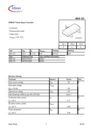
PROFET® BTS 410 D2<br />
Product Summary<br />
Overvoltage protection V bb(AZ) 65 V<br />
Operating voltage Vbb(on) 4.7 ... 42 V<br />
On-state resistance RON 220 mΩ<br />
Load current (ISO) IL(ISO) 1.8 A<br />
Current limitation IL(SCr) 5 A<br />
Standard<br />
General Description<br />
N channel vertical power FET with charge pump, ground referenced CMOS compatible input and diagnostic<br />
feedback, monolithically integrated in <strong>Smart</strong> SIPMOS® technology. Fully protected by embedded protection<br />
functions.<br />
5<br />
TO-220AB/5<br />
1<br />
Straight leads<br />
5<br />
1<br />
SMD<br />
5<br />
Voltage<br />
source<br />
Overvoltage<br />
protection<br />
Current<br />
limit<br />
Gate<br />
protection<br />
+ V bb<br />
3<br />
V Logic<br />
2<br />
IN<br />
ESD<br />
Voltage<br />
sensor<br />
Logic<br />
Charge pump<br />
Level shifter<br />
Rectifier<br />
Limit for<br />
unclamped<br />
ind. loads<br />
Open load<br />
detection<br />
Temperature<br />
sensor<br />
OUT<br />
5<br />
Load<br />
4<br />
ST<br />
1<br />
GND<br />
Signal GND<br />
Short circuit<br />
detection<br />
PROFET ®<br />
Load GND<br />
1) With external current limit (e.g. resistor R GND =150 Ω) in GND connection, resistors in series with IN and ST<br />
connections, reverse load current limited by connected load.<br />
Semiconductor Group 1 03.97
Pin Symbol Function<br />
1 GND - Logic ground<br />
BTS 410 D2<br />
2 IN I Input, activates the power switch in case of logical high signal<br />
3 Vbb + Positive power supply voltage,<br />
the tab is shorted to this pin<br />
4 ST S Diagnostic feedback, low on failure<br />
5 OUT<br />
(Load, L)<br />
O Output to the load<br />
Maximum Ratings at Tj = 25 °C unless otherwise specified<br />
Parameter Symbol Values Unit<br />
Supply voltage (overvoltage protection see page 3) V bb 65 V<br />
Load dump protection 2) V LoadDump = U A + V s , U A = 13.5 V V<br />
4) Load dump 100 V<br />
R I<br />
3)<br />
= 2 Ω, R L = 6.6 Ω, t d = 400 ms, IN= low or high<br />
Load current (Short circuit current, see page 4) I L self-limited A<br />
Operating temperature range<br />
T j<br />
-40 ...+150 °C<br />
Storage temperature range<br />
T stg -55 ...+150<br />
<strong>Power</strong> dissipation (DC), T C ≤ 25 °C P tot 50 W<br />
Inductive load switch-off energy dissipation, single pulse<br />
V bb = 12V, T j,start = 150°C, T C = 150°C const.<br />
I L = 1.8 A, Z L = 2.3 H, 0 Ω: E AS 4.5 J<br />
Electrostatic discharge capability (ESD)<br />
(Human Body Model)<br />
IN:<br />
all other pins:<br />
V ESD 1<br />
2<br />
kV<br />
acc. MIL-STD883D, method 3015.7 and ESD assn. std. S5.1-1993<br />
Input voltage (DC) V IN -0.5 ... +6 V<br />
Current through input pin (DC)<br />
I IN<br />
±5.0 mA<br />
Current through status pin (DC)<br />
I ST ±5.0<br />
see internal circuit diagrams page 6<br />
Thermal Characteristics<br />
--<br />
Parameter and Conditions Symbol Values Unit<br />
min typ max<br />
Thermal resistance<br />
chip - case: R thJC<br />
-- 2.5 K/W<br />
junction - ambient (free air): R thJA -- -- 75<br />
SMD version, device on PCB 5) : -- 35 --<br />
2) Supply voltages higher than V bb(AZ) require an external current limit for the GND and status pins, e.g. with a<br />
150 Ω resistor in the GND connection and a 15 kΩ resistor in series with the status pin. A resistor for the<br />
protection of the input is integrated.<br />
3) R I = internal resistance of the load dump test pulse generator<br />
4) V Load dump is setup without the DUT connected to the generator per ISO 7637-1 and DIN 40839<br />
5) Device on 50mm*50mm*1.5mm epoxy PCB FR4 with 6cm 2 (one layer, 70µm thick) copper area for V bb<br />
connection. PCB is vertical without blown air.<br />
Semiconductor Group 2
BTS 410 D2<br />
Electrical Characteristics<br />
Parameter and Conditions Symbol Values Unit<br />
at Tj = 25 °C, V bb = 12 V unless otherwise specified min typ max<br />
Load <strong>Switch</strong>ing Capabilities and Characteristics<br />
On-state resistance (pin 3 to 5)<br />
I L = 1.6 A<br />
T j =25 °C:<br />
T j =150 °C:<br />
R ON -- 190<br />
390<br />
Nominal load current, ISO Norm (pin 3 to 5)<br />
V ON = 0.5 V, T C = 85 °C I L(ISO) 1.6 1.8 -- A<br />
Output current (pin 5) while GND disconnected or<br />
GND pulled up, Vbb=30 V, V IN = 0, see diagram<br />
I L(GNDhigh) -- -- 1 mA<br />
page 7, Tj =-40...+150°C<br />
Turn-on time IN to 90% V OUT :<br />
Turn-off time IN to 10% V OUT :<br />
R L = 12 Ω, Tj =-40...+150°C<br />
Slew rate on<br />
10 to 30% V OUT , R L = 12 Ω, Tj =-40...+150°C<br />
Slew rate off<br />
70 to 40% V OUT , R L = 12 Ω, Tj =-40...+150°C<br />
t on<br />
12<br />
t off 5<br />
--<br />
--<br />
220<br />
440<br />
125<br />
85<br />
mΩ<br />
µs<br />
dV /dt on -- -- 3 V/µs<br />
-dV/dt off -- -- 6 V/µs<br />
Operating Parameters<br />
Operating voltage 6) Tj =-40...+150°C: V bb(on) 4.7 -- 42 V<br />
Undervoltage shutdown<br />
Tj =25°C: V bb(under) 2.9 -- 4.5 V<br />
Tj =-40...+150°C:<br />
2.7 -- 4.7<br />
Undervoltage restart Tj =-40...+150°C: V bb(u rst) -- -- 4.9 V<br />
Undervoltage restart of charge pump<br />
V bb(ucp) -- 5.6 6.0 V<br />
see diagram page 12<br />
Undervoltage hysteresis<br />
∆V bb(under) = V bb(u rst) - V bb(under)<br />
∆V bb(under) -- 0.1 -- V<br />
Overvoltage shutdown Tj =-40...+150°C: V bb(over) 42 -- 52 V<br />
Overvoltage restart Tj =-40...+150°C: V bb(o rst) 40 -- -- V<br />
Overvoltage hysteresis Tj =-40...+150°C: ∆V bb(over) -- 0.1 -- V<br />
Overvoltage protection 7) Tj =-40...+150°C: V bb(AZ) 65 70 -- V<br />
I bb =4 mA<br />
Standby current (pin 3)<br />
V IN =0, I ST ≤0,<br />
Leakage output current (included in I bb(off) )<br />
VIN=0<br />
Operating current (Pin 1) 8) , V IN =5 V,<br />
Tj =-40...+150°C<br />
T j =-40...+25°C:<br />
T j = 150°C:<br />
Semiconductor Group 3<br />
I bb(off) --<br />
--<br />
10<br />
18<br />
15<br />
25<br />
µA<br />
I L(off) -- -- 20 µA<br />
I GND -- 1 2.1 mA<br />
6) At supply voltage increase up to V bb = 5.6 V typ without charge pump, V OUT ≈V bb - 2 V<br />
7) Meassured without load. See also VON(CL) in table of protection functions and circuit diagram page 7.
BTS 410 D2<br />
Parameter and Conditions Symbol Values Unit<br />
at Tj = 25 °C, V bb = 12 V unless otherwise specified min typ max<br />
Protection Functions<br />
Initial peak short circuit current limit (pin 3 to 5) 9) ,<br />
( max 450 µs if V ON > V ON(SC) )<br />
T j =-40°C:<br />
T j =25°C:<br />
T j =+150°C:<br />
Overload shutdown current limit<br />
I L(SCp)<br />
I L(SCr)<br />
9 -- 23<br />
-- 12 --<br />
4 -- 15<br />
V ON = 8 V, T j = T jt (see timing diagrams, page 10) -- 5 -- A<br />
Short circuit shutdown delay after input pos. slope<br />
V ON > V ON(SC) ,<br />
T j =-40..+150°C: t d(SC) -- -- 450 µs<br />
min value valid only, if input "low" time exceeds 60 µs<br />
Output clamp (inductive load switch off)<br />
at V OUT = V bb - V ON(CL) I L = 40 mA, T j =-40..+150°C: V ON(CL) 61 68 73 V<br />
I L = 1 A, T j =-40..+150°C: -- -- 75<br />
Short circuit shutdown detection voltage<br />
(pin 3 to 5) V ON(SC) -- 8.5 -- V<br />
Thermal overload trip temperature T jt 150 -- -- °C<br />
Thermal hysteresis ∆T jt -- 10 -- K<br />
Reverse battery (pin 3 to 1) 10) -V bb -- -- 32 V<br />
A<br />
Diagnostic Characteristics<br />
Open load detection current<br />
(on-condition)<br />
T j =-40 ..150°C:<br />
I L (OL)<br />
2 -- 150<br />
mA<br />
8) Add I ST , if I ST > 0, add I IN , if V IN >5.5 V<br />
9) Short circuit current limit for max. duration of t d(SC) max =450 µs, prior to shutdown<br />
10) Requires 150 Ω resistor in GND connection. The reverse load current through the intrinsic drain-source<br />
diode has to be limited by the connected load. Note that the power dissipation is higher compared to normal<br />
operating conditions due to the voltage drop across the intrinsic drain-source diode. The temperature<br />
protection is not active during reverse current operation! Input and Status currents have to be limited (see<br />
max. ratings page 2 and circuit page 7).<br />
Semiconductor Group 4
BTS 410 D2<br />
Parameter and Conditions Symbol Values Unit<br />
at Tj = 25 °C, V bb = 12 V unless otherwise specified min typ max<br />
Input and Status Feedback 11)<br />
Input turn-on threshold voltage T j =-40..+150°C: V IN(T+) 1.5 -- 2.4 V<br />
Input turn-off threshold voltage T j =-40..+150°C: V IN(T-) 1.0 -- -- V<br />
Input threshold hysteresis ∆ V IN(T) -- 0.5 -- V<br />
Off state input current (pin 2), V IN = 0.4 V I IN(off) 1 -- 30 µA<br />
On state input current (pin 2), V IN = 5 V I IN(on) 10 25 70 µA<br />
Status invalid after positive input slope<br />
t d(ST SC) -- -- 450 µs<br />
(short circuit)<br />
Tj=-40 ... +150°C:<br />
Status invalid after positive input slope<br />
t d(ST) 300 -- 1400 µs<br />
(open load)<br />
Tj=-40 ... +150°C:<br />
Status output (CMOS)<br />
T j =-40...+150°C, I ST = - 50 µA:<br />
T j =-40...+150°C, I ST = +1.6 mA:<br />
Max. status current for<br />
current source (out):<br />
valid status output, current sink (in) :<br />
T j =-40...+150°C<br />
V ST(high)<br />
12)<br />
V ST(low)<br />
-I ST<br />
+I ST<br />
13)<br />
4.4<br />
--<br />
--<br />
--<br />
5.1<br />
--<br />
--<br />
--<br />
6.5<br />
0.4<br />
0.25<br />
1.6<br />
V<br />
mA<br />
11) If a ground resistor R GND is used, add the voltage drop across this resistor.<br />
12) VSt high ≈ V bb during undervoltage shutdown<br />
13) No current sink capability during undervoltage shutdown<br />
Semiconductor Group 5
BTS 410 D2<br />
Truth Table<br />
Normal<br />
operation<br />
Open load<br />
Input- Output Status<br />
level level 412<br />
B2<br />
L<br />
H<br />
L<br />
H<br />
L<br />
H<br />
L<br />
H<br />
L<br />
H<br />
L<br />
H<br />
L<br />
H<br />
L<br />
H<br />
14)<br />
H<br />
L<br />
L<br />
H<br />
H<br />
L<br />
L<br />
L<br />
L<br />
L<br />
L<br />
410<br />
D2<br />
H H<br />
H H<br />
L H<br />
H L<br />
H H<br />
L L<br />
L H<br />
H H (L 15) )<br />
L L<br />
L L<br />
L 16) L 16)<br />
L 16) L 16)<br />
L L<br />
L L<br />
410<br />
E2/F2<br />
H<br />
H<br />
H<br />
L<br />
H<br />
L<br />
H<br />
H (L 15) )<br />
L<br />
L<br />
H<br />
H<br />
H<br />
H<br />
410<br />
G2<br />
H<br />
H<br />
H<br />
L<br />
H<br />
H<br />
H<br />
H (L 15) )<br />
L<br />
L<br />
H<br />
H<br />
H<br />
H<br />
L = "Low" Level X = don't care Z = high impedance, potential depends on external circuit<br />
H = "High" Level Status signal after the time delay shown in the diagrams (see fig 5. page 11...12)<br />
Terms<br />
Status output<br />
410<br />
H2<br />
H<br />
H<br />
L<br />
H<br />
H<br />
L<br />
L<br />
H<br />
L<br />
L<br />
H<br />
H<br />
H<br />
H<br />
I bb<br />
3<br />
I IN<br />
V<br />
IN bb<br />
2<br />
I L V ON<br />
PROFET OUT<br />
I ST<br />
5<br />
ST<br />
4<br />
V V GND<br />
IN ST<br />
V 1<br />
bb I GND<br />
V OUT<br />
R GND<br />
Input circuit (ESD protection)<br />
GND<br />
V Logic<br />
ESD-<br />
ZDI1<br />
ZDI2<br />
ESD-<br />
ZD<br />
Zener diode: 6 V typ., max 5.0 mA, V Logic 5 V typ,<br />
ESD zener diodes are not to be used as voltage clamp<br />
at DC conditions. Operation in this mode may result in<br />
a drift of the zener voltage (increase of up to 1 V).<br />
ST<br />
IN<br />
R<br />
I<br />
Short circuit<br />
to GND<br />
Short circuit<br />
to V bb<br />
Overtemperature<br />
Undervoltage<br />
Overvoltage<br />
I<br />
I<br />
GND<br />
ZDI1 6 V typ., ESD zener diodes are not to be used as<br />
voltage clamp at DC conditions. Operation in this mode<br />
may result in a drift of the zener voltage (increase of up<br />
to 1 V).<br />
14) <strong>Power</strong> Transistor off, high impedance, versions BTS 410H, BTS 412B: internal pull up current source for<br />
open load detection.<br />
15) Low resistance short Vbb to output may be detected in ON-state by the no-load-detection<br />
16) No current sink capability during undervoltage shutdown<br />
Semiconductor Group 6
BTS 410 D2<br />
Short circuit detection<br />
Fault Condition: V ON > 8.5 V typ.; IN high<br />
Open-load detection<br />
ON-state diagnostic condition: V ON < R ON * I L(OL) ; IN<br />
high<br />
+ V bb<br />
+ V bb<br />
V<br />
ON<br />
ON<br />
V ON<br />
Logic<br />
unit<br />
Short circuit<br />
detection<br />
OUT<br />
Logic<br />
unit<br />
Open load<br />
detection<br />
OUT<br />
Inductive and overvoltage output clamp<br />
+ V bb<br />
V Z<br />
GND disconnect<br />
V ON<br />
3<br />
GND<br />
VON clamped to 68 V typ.<br />
PROFET<br />
OUT<br />
2<br />
4<br />
IN<br />
ST<br />
V<br />
bb<br />
PROFET<br />
GND<br />
OUT<br />
5<br />
V V V 1<br />
bb IN ST<br />
V GND<br />
Overvolt. and reverse batt. protection<br />
R IN<br />
R ST<br />
IN<br />
ST<br />
V Z1<br />
Logic<br />
R GND<br />
V Z2<br />
PROFET<br />
GND<br />
Signal GND<br />
+ V bb<br />
V Z1 = 6.2 V typ., V Z2 = 70 V typ., R GND = 150 Ω, R IN ,<br />
RST= 15 kΩ<br />
Any kind of load. In case of Input=high is V OUT ≈ V IN - V IN(T+) .<br />
Due to V GND >0, no V ST = low signal available.<br />
GND disconnect with GND pull up<br />
3<br />
V<br />
IN bb<br />
2<br />
PROFET OUT<br />
5<br />
4<br />
ST<br />
GND<br />
V V IN ST<br />
V GND<br />
1<br />
Any kind of load. If V GND > VIN - V IN(T+) device stays off<br />
Due to V GND >0, no V ST = low signal available.<br />
Semiconductor Group 7
Vbb disconnect with energized inductive<br />
load<br />
high<br />
IN<br />
ST<br />
V bb<br />
1<br />
2<br />
4<br />
3<br />
V<br />
bb<br />
PROFET<br />
GND<br />
OUT<br />
Normal load current can be handled by the PROFET<br />
itself.<br />
Vbb disconnect with charged external<br />
inductive load<br />
5<br />
with an approximate solution for R L > 0 Ω:<br />
BTS 410 D2<br />
E AS = I L· L<br />
2·R bb L·(V + |V I<br />
OUT(CL)|)· ln L·R L<br />
(1+<br />
|V OUT(CL) | )<br />
Maximum allowable load inductance for<br />
a single switch off<br />
L = f (I L ); T j,start = 150°C,T C = 150°C const.,<br />
V bb = 12 V, R L = 0 Ω<br />
L [mH]<br />
10000<br />
1000<br />
100<br />
high<br />
V bb<br />
2<br />
4<br />
S<br />
IN<br />
ST<br />
3<br />
V<br />
bb<br />
PROFET<br />
GND<br />
1<br />
OUT<br />
If other external inductive loads L are connected to the PROFET,<br />
additional elements like D are necessary.<br />
Inductive Load switch-off energy<br />
dissipation<br />
E bb<br />
5<br />
D<br />
10<br />
1<br />
1 2 3 4 5 6<br />
I L [A]<br />
Typ. transient thermal impedance chip case<br />
Z thJC = f(t p , D), D=t p /T<br />
Z thJC [K/W]<br />
10<br />
E AS<br />
IN<br />
V<br />
bb<br />
E Load<br />
1<br />
PROFET<br />
OUT<br />
=<br />
ST<br />
GND<br />
Energy stored in load inductance:<br />
L<br />
Z L { RL<br />
E<br />
L<br />
E R<br />
0.1<br />
D=<br />
0.5<br />
0.2<br />
0.1<br />
0.05<br />
0.02<br />
0.01<br />
0<br />
E L = 1 /2·L·I 2 L<br />
While demagnetizing load inductance, the energy<br />
dissipated in PROFET is<br />
E AS = E bb + E L - E R = ∫ V ON(CL)·i L (t) dt,<br />
0.01<br />
1E-5 1E-4 1E-3 1E-2 1E-1 1E0 1E1<br />
t p [s]<br />
Semiconductor Group 8
Options Overview<br />
BTS 410 D2<br />
all versions: High-side switch, Input protection, ESD protection, load dump and<br />
reverse battery protection with 150 Ω in GND connection, protection against loss of<br />
ground<br />
Type BTS 412 B2 410D2 410E2 410F2 410G2 410H2 307 308<br />
Logic version B D E F G H<br />
Overtemperature protection with hysteresis<br />
Tj >150 °C, latch function 17)18)<br />
Tj >150 °C, with auto-restart on cooling<br />
Short circuit to GND protection<br />
switches off when V ON >3.5 V typ. and V bb > 7 V<br />
typ 17) (when first turned on after approx. 150 µs)<br />
switches off when V ON >8.5 V typ. 17)<br />
(when first turned on after approx. 150 µs)<br />
Achieved through overtemperature protection<br />
Open load detection<br />
in OFF-state with sensing current 30 µA typ.<br />
in ON-state with sensing voltage drop across<br />
power transistor<br />
X<br />
X<br />
X<br />
X<br />
X X X X<br />
X<br />
X<br />
X<br />
X X X X<br />
X<br />
X<br />
X<br />
X<br />
X<br />
X<br />
X X X<br />
Undervoltage shutdown with auto restart X X X X X X X X<br />
Overvoltage shutdown with auto restart 19) X X X X X X - X<br />
Status feedback for<br />
overtemperature<br />
short circuit to GND<br />
short to V bb<br />
open load<br />
undervoltage<br />
overvoltage<br />
Status output type<br />
CMOS<br />
Open drain<br />
X<br />
X<br />
X<br />
X<br />
X<br />
X<br />
X<br />
X<br />
X<br />
- 20)<br />
X<br />
X<br />
X<br />
X<br />
X<br />
X<br />
- 20)<br />
X<br />
-<br />
-<br />
X<br />
X<br />
- 20)<br />
X<br />
-<br />
-<br />
X<br />
-<br />
- 20)<br />
X<br />
-<br />
-<br />
X<br />
X<br />
X<br />
X<br />
-<br />
-<br />
X<br />
X<br />
X<br />
X<br />
X<br />
-<br />
X X X X X X<br />
Output negative voltage transient limit<br />
(fast inductive load switch off)<br />
to V bb - V ON(CL) X X X X X X X X<br />
Load current limit<br />
high level (can handle loads with high inrush currents)<br />
low level (better protection of application)<br />
X X X<br />
X<br />
X<br />
X<br />
X<br />
-<br />
-<br />
X X X X X<br />
Protection against loss of GND X X X X X X X X<br />
17) Latch except when Vbb -V OUT < V ON(SC) after shutdown. In most cases VOUT = 0 V after shutdown (V OUT ≠<br />
0 V only if forced externally). So the device remains latched unless V bb < V ON(SC)<br />
(see page 4). No latch<br />
between turn on and t d(SC) .<br />
18) With latch function. Reseted by a) Input low, b) Undervoltage<br />
19) No auto restart after overvoltage in case of short circuit<br />
20) Low resistance short Vbb to output may be detected in ON-state by the no-load-detection<br />
Semiconductor Group 9
Timing diagrams<br />
Figure 1a: V bb turn on:<br />
Figure 2b: <strong>Switch</strong>ing an inductive load<br />
BTS 410 D2<br />
IN<br />
IN<br />
V<br />
bb<br />
t d(bb IN)<br />
ST<br />
t d(ST)<br />
*)<br />
V<br />
OUT<br />
V<br />
OUT<br />
A<br />
ST CMOS<br />
A<br />
in case of too early VIN=high the device may not turn on (curve A)<br />
t d(bb IN) approx. 150 µs<br />
Figure 2a: <strong>Switch</strong>ing a lamp,<br />
t<br />
I<br />
L<br />
I L(OL)<br />
*) if the time constant of load is too large, open-load-status may<br />
occur<br />
Figure 3a: Turn on into short circuit,<br />
t<br />
IN<br />
IN<br />
ST<br />
ST<br />
V<br />
OUT<br />
V<br />
OUT<br />
t d(SC)<br />
I<br />
L<br />
I<br />
L<br />
t<br />
t<br />
td(SC) approx. -- µs if V bb - V OUT > 8.5 V typ.<br />
Semiconductor Group 10
Figure 3b: Turn on into overload,<br />
IN<br />
Figure 4a: Overtemperature,<br />
Reset if (IN=low) and (T j
Figure 5b: Open load: detection in ON-state, open<br />
load occurs in on-state<br />
BTS 410 D2<br />
Figure 6b: Undervoltage restart of charge pump<br />
V on<br />
V ON(CL)<br />
IN<br />
ST<br />
t d(ST OL1)<br />
t d(ST OL2)<br />
V<br />
OUT<br />
off-state<br />
on-state<br />
V bb(over)<br />
off-state<br />
V bb(u rst)<br />
V bb(o rst)<br />
I<br />
L<br />
normal<br />
open<br />
normal<br />
V<br />
bb(under)<br />
V bb(u cp)<br />
t<br />
charge pump starts at V bb(ucp) =5.6 V typ.<br />
V bb<br />
t d(ST OL1) = tbd µs typ., t d(ST OL2) = tbd µs typ<br />
Figure 7a: Overvoltage:<br />
Figure 6a: Undervoltage:<br />
IN<br />
IN<br />
V<br />
bb<br />
V<br />
bb<br />
V<br />
ON(CL) V bb(over)<br />
V bb(o rst)<br />
V<br />
bb(under)<br />
Vbb(u cp)<br />
V<br />
bb(u rst)<br />
V<br />
OUT<br />
VOUT<br />
ST<br />
ST CMOS<br />
t<br />
t<br />
if V bb > V bb(AZ) increase of V ST due to GND resistor voltage.<br />
Semiconductor Group 12
Figure 9a: Overvoltage at short circuit shutdown:<br />
BTS 410 D2<br />
IN<br />
V<br />
bb<br />
V bb(o rst)<br />
V<br />
OUT<br />
Output short to GND<br />
short circuit shutdown<br />
I L<br />
ST<br />
t<br />
Overvoltage due to power line inductance. No overvoltage autorestart<br />
of PROFET after short circuit shutdown.<br />
Semiconductor Group 13
Package and Ordering Code<br />
All dimensions in mm<br />
Standard TO-220AB/5<br />
BTS 410 D2<br />
Ordering code<br />
Q67060-S6101-A2<br />
BTS 410 D2<br />
SMD TO-220AB/5, Opt. E3062 Ordering code<br />
BTS410D2 E3062A T&R: Q67060-S6101-A4<br />
TO-220AB/5, Option E3043 Ordering code<br />
BTS 410 D2 E3043<br />
Q67060-S6101-A3<br />
Semiconductor Group 14