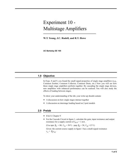
Experiment 10 - Multistage Amplifiers
Experiment 10 - Multistage Amplifiers
Experiment 10 - Multistage Amplifiers

Create successful ePaper yourself
Turn your PDF publications into a flip-book with our unique Google optimized e-Paper software.
<strong>Experiment</strong> <strong>10</strong> -<br />
<strong>Multistage</strong> <strong>Amplifiers</strong><br />
W.T. Yeung, J.C. Rudell, and R.T. Howe<br />
UC Berkeley EE <strong>10</strong>5<br />
1.0 Objective<br />
In Exps. 8 and 9, you found the small signal properties of single stage amplifiers (e.g.,<br />
Common Emitter, Common Collector, Common Drain, etc.) Now you will see how<br />
these single stage amplifiers perform together. By cascading the single stage devices,<br />
new amplifiers with enhanced performance can be realized. You will also study the<br />
effects of loading between stages.<br />
To show your understanding of the lab, your write-up should contain:<br />
• A discussion on how single stages interact together<br />
• A discussion on interstage loading based on 2-port models<br />
2.0 Prelab<br />
• H & S: Chapter 9<br />
• For the Cascode Circuit in figure 1, calculate the gain, input resistance and output<br />
resistance for a supply current of I SUP = 1 mA.<br />
(Use npn: β n = 80, V An = 50 V, - pnp: β p = 30, V Ap =15 V.)<br />
Given: the current-source supply in figure 1 has a small-signal resistance<br />
r oc = β p r op .<br />
1 of 5
Procedure<br />
FIGURE 1.<br />
Cascode Amplifier with Current Source Supply<br />
V CC<br />
I SUP<br />
<strong>10</strong>µF<br />
v OUT<br />
M3501<br />
250kΩ<br />
Q 2<br />
V BIAS<br />
1 MΩ<br />
v IN<br />
Q 1<br />
M3501<br />
3.0 Procedure<br />
3.1 The Cascode<br />
The Cascode circuit is nothing more than a Common Emitter - Common Base (or Common<br />
Source - Common Gate) cascade. Figure 1 above shows a simplified cascode with<br />
a current source load.<br />
The 2 port model for the cascode is shown below<br />
FIGURE 2.<br />
2-Port Representation of Cascode<br />
R in G m R out R in -i in2 R out<br />
R L<br />
Common Emitter Stage<br />
Common Base Stage<br />
2 of 5 <strong>Experiment</strong> <strong>10</strong> - <strong>Multistage</strong> <strong>Amplifiers</strong>
Procedure<br />
In your lab, the cascode circuit will include extra biasing circuits as shown in figure 3.<br />
These circuits make use of DC feedback (coupled through the external low-pass filter),<br />
in order to stabilize this high-gain circuit. After simplification, figure 3 reduces to the<br />
basic cascode amplifier in figure 1.<br />
1. Set up the circuit from Lab Chip 4 as shown in figure 3. Let R Bias be <strong>10</strong> kΩ.and C in<br />
be <strong>10</strong> µF. Let V CC be set at 5V. Note: The user just needs to furnish the external elements<br />
in the box. (the elements in the dashed “boxes” in figure 3).<br />
2. Determine the bias current and DC voltage at V OUT . Using figure 3, what are the<br />
maximum and minimum DC voltages that V OUT can swing to while keeping all the<br />
devices in the forward active region. Compare with measurements of output clipping<br />
levels.<br />
3. Using the oscilloscope, find the gain v out /v in . Use a 5 kHz sine wave with an amplitude<br />
of 200 mV. If the signal at the output is clipped, decrease the input amplitude<br />
until no clipping occurs.<br />
4. Calculate the input resistance and output resistance for the cascode. Using the calculated<br />
value of the input resistance, you can calculate how much of the input voltage<br />
is attenuated. Determine the gain of the cascode v out /v in . How does the cascode compare<br />
to the Common Emitter in terms of input resistance, output resistance and voltage<br />
gain? Optional: measure the input and the output resistances.<br />
FIGURE 3. Bipolar Cascode with DC Feedback Biasing (Lab Chip 4)<br />
Off-chip components: input signal, setting DC<br />
operating point of cascode<br />
VCC<br />
PIN 28<br />
Q 5 Q<br />
M3511<br />
6<br />
M3511<br />
I BIAS R Bias<br />
R 5<br />
M3511<br />
250Ω<br />
Q 4<br />
PIN 17<br />
v OUT R 4<br />
Q 7<br />
M3501<br />
R 250Ω<br />
S = 1 MΩ C<br />
PIN 16 v in<br />
in M3501<br />
M 9<br />
Q 3<br />
R<br />
R lp = 5MegΩ PIN 15<br />
v 3<br />
IN<br />
250Ω<br />
PIN 19<br />
M<br />
Q 2<br />
2 Q 1<br />
PIN 18<br />
M3501<br />
C<br />
R R 2 = 90kΩ<br />
1 = 90kΩ<br />
M3501<br />
lp = <strong>10</strong>u<br />
R 6 = 3.75kΩ<br />
GND<br />
PIN 14<br />
<strong>Experiment</strong> <strong>10</strong> - <strong>Multistage</strong> <strong>Amplifiers</strong> 3 of 5
Procedure<br />
Lab Tip<br />
Find the DC voltage at v OUT (PIN 17) and make sure that Q 3 and Q 4 are not saturated. If<br />
they are, get a new chip.The circuit takes about <strong>10</strong> - 20 seconds to stabilize. Be patient.<br />
5. Perform a SPICE analysis on the Cascode in figure 1 (figure 3 is extra credit) and<br />
compare your results with simulation.<br />
3.2 Cascading Stages<br />
1. While leaving the Cascode intact, build the common emitter as shown in figure 4.<br />
Set R BIAS (CEBIASP) to be a potentiometer and adjust it until the output is at 2.5V.<br />
(This is merely the same procedure as the common emitter circuit in Exp. 8.) Find<br />
the bias current through R BIAS . Does the DC voltage at V OUT confirm the fact that I C =<br />
I BIAS ? Find the gain of the Common Emitter.<br />
2. Now cascade the two stages together with the use of the <strong>10</strong> µF coupling capacitor.<br />
What is its function? (Hint: look at the DC voltage at both sides of the capacitor)<br />
What would happen if the capacitor were not present? Change the amplitude of the<br />
sinusoid to 50 mV.<br />
3. Find the gain for the cascade. Measure the gain v out1 / v in . Why is it reduced?<br />
FIGURE 4.<br />
Cascode - Common Emitter Cascade<br />
Lab Chip 4<br />
PIN 28<br />
V CC<br />
=<br />
5V<br />
PIN 28<br />
V CC = 5 V<br />
I SUP<br />
v OUT1<br />
PIN 26<br />
R C<br />
= <strong>10</strong>kΩ<br />
v OUT2<br />
PIN 25<br />
I C is controlled by<br />
R BIAS between CE_BIAS<br />
(PIN 27) and V CC .<br />
M3501<br />
Q 2<br />
PIN 17<br />
<strong>10</strong> µF<br />
v b<br />
Ground = PIN 14<br />
PIN 19<br />
V BIAS<br />
v in<br />
+ _<br />
v IN<br />
Q 1<br />
M3501<br />
Lab Chip 3<br />
4 of 5 <strong>Experiment</strong> <strong>10</strong> - <strong>Multistage</strong> <strong>Amplifiers</strong>
Optional <strong>Experiment</strong>s<br />
4. Draw the 2 port models for the cascaded amplifier in Fig. 4. Comment on the overall<br />
gain and the loading between stages.<br />
4.0 Optional <strong>Experiment</strong>s<br />
4.1 Common Collector as a Buffering Stage<br />
1. Leaving the cascode and common emitter circuit intact, we now insert a Common<br />
Collector as an intermediate stage between the Cascode and Common Emitter. Find<br />
the gain of this new circuit. For the Common Collector, set R BIAS = <strong>10</strong>0 kΩ. For measuring<br />
input attenuation, the source resistance may have to be increased over the<br />
value in figure 3. Lower the amplitude of the input sinusoid and reduce the source<br />
resistance as necessary to avoid clipping at the output.<br />
2. Draw the 2-port models for this Cascode-CC-CE configuration. Comment on the<br />
gain and the interstage loading.<br />
FIGURE 5. Common Collector (Emitter Follower) Voltage Buffer (Lab Chip 4)<br />
V CC<br />
=<br />
5V<br />
I BIAS is controlled by R BIAS<br />
between EF_BIAS (PIN 25)<br />
and V CC (PIN 28) on Lab<br />
Chip 4<br />
PIN 23<br />
v b<br />
PIN 24<br />
PIN 26<br />
(chip 3)<br />
R C<br />
=<br />
<strong>10</strong>kΩ<br />
v OUT<br />
PIN 25 (chip 3)<br />
I BIAS<br />
<strong>10</strong> µF<br />
v in3<br />
Ground = PIN 14<br />
<strong>Experiment</strong> <strong>10</strong> - <strong>Multistage</strong> <strong>Amplifiers</strong> 5 of 5