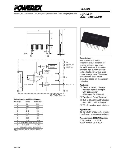
Hybrid IC IGBT Gate Driver VLA504 - Powerex
Hybrid IC IGBT Gate Driver VLA504 - Powerex
Hybrid IC IGBT Gate Driver VLA504 - Powerex

Create successful ePaper yourself
Turn your PDF publications into a flip-book with our unique Google optimized e-Paper software.
<strong>VLA504</strong><br />
<strong>Powerex</strong>, Inc., 173 Pavilion Lane, Youngwood, Pennsylvania 15697-1800 (724) 925-7272<br />
<strong>Hybrid</strong> <strong>IC</strong><br />
<strong>IGBT</strong> <strong>Gate</strong> <strong>Driver</strong><br />
A<br />
C<br />
B<br />
K<br />
14<br />
13<br />
180Ω<br />
D<br />
Outline Drawing and Circuit Diagram<br />
Dimensions Inches Millimeters<br />
A 2.0 51.0<br />
B 1.02 26.0<br />
C 0.4 10.0<br />
D 0.45 11.5<br />
E 0.12 3.0<br />
F 0.3 7.5<br />
G 0.25 6.5<br />
H 0.10 2.54<br />
J 0.02+0.006/-0.004 0.5+0.15/-0.1<br />
K 0.18±0.06 4.5±1.5<br />
L 0.01+0.01/-0.004 0.25+0.2/-0.1<br />
Note: All dimensions listed are maximums except H, J,<br />
K, and L.<br />
1<br />
OPTO COUPLER<br />
J<br />
INTERFACE<br />
H<br />
LATCH<br />
14<br />
TIMER AND<br />
RESET<br />
CIRCUIT<br />
GATE<br />
SHUTDOWN<br />
CIRCUIT<br />
G<br />
DETECT<br />
CIRCUIT<br />
E<br />
L<br />
F<br />
3 , 7 , 9 , 10 PIN : NC<br />
4<br />
2<br />
1<br />
5<br />
8<br />
6<br />
V CC<br />
CONTROL PIN<br />
FOR t trip<br />
DETECT PIN<br />
V O<br />
FAULT OUTPUT<br />
V EE<br />
Description:<br />
The <strong>VLA504</strong> is a hybrid<br />
integrated circuit designed to<br />
provide optimum gate drive<br />
for <strong>IGBT</strong> modules. This device<br />
provides high current optically<br />
isolated gate drive with a large<br />
output voltage swing. The driver<br />
also provides short circuit<br />
protection based on desaturation<br />
detection.<br />
Features:<br />
£ Electrical Isolation Voltage<br />
Between Input and Output<br />
with Opto-coupler<br />
(2500 Vrms for 1 Minute)<br />
£ Two Supply <strong>Driver</strong> Topology<br />
£ Built-in Short-Circuit Protection<br />
(With a Pin for Fault Output)<br />
£ TTL Compatible Input Interface<br />
Application:<br />
To drive <strong>IGBT</strong> modules for inverter<br />
or AC servo systems applications<br />
Recommended <strong>IGBT</strong> Modules:<br />
600V module up to 200A<br />
1200V module up to 100A<br />
Rev. 2/06<br />
1
<strong>Powerex</strong>, Inc., 173 Pavilion Lane, Youngwood, Pennsylvania 15697-1800 (724) 925-7272<br />
<strong>VLA504</strong><br />
<strong>Hybrid</strong> <strong>IC</strong> <strong>IGBT</strong> <strong>Gate</strong> <strong>Driver</strong><br />
Absolute Maximum Ratings, T a = 25°C unless otherwise specified<br />
Characteristics Symbol <strong>VLA504</strong> Units<br />
Supply Voltage, DC V CC 18 Volts<br />
V EE -15 Volts<br />
Input Signal Voltage (Applied between Pin 13 - 14, 50% Duty Cycle, Pulse Width 1ms) V i -1 ~ +7 Volts<br />
Output Voltage (When the Output Voltage is "H") V O V CC Volts<br />
Output Current I OHP -3 Amperes<br />
(Pulse Width 2µs, f ≤ 20kHz) I OLP 3 Amperes<br />
Isolation Voltage (Sine Wave Voltage 60Hz, for 1 Minute) V ISO 2500 V rms<br />
Case Temperature T C 85 °C<br />
Operating Temperature (No Condensation Allowable) T opr -20 ~ +60 °C<br />
Storage Temperature (No Condensation Allowable)* T stg -25 ~ +100 °C<br />
Fault Output Current (Applied Pin 8) I FO 20 mA<br />
Input Voltage at Pin 1 (Applied Pin 1) V R1 50 Volts<br />
*Differs from H/C condition.<br />
Electrical and Mechanical Characteristics, T a = 25°C unless otherwise specified, V CC = 15V, V EE = -10V)<br />
Characteristics Symbol Test Conditions Min. Typ. Max. Units<br />
Supply Voltage V CC Recommended Range 14 15 — Volts<br />
V EE Recommended Range -7 — -10 Volts<br />
Pull-up Voltage on Primary Side V IN Recommended Range 4.75 5 5.25 Volts<br />
"H" Input Current I IH Recommended Range 15.2 16 19 mA<br />
Switching Frequency f Recommended Range — — 20 kHz<br />
<strong>Gate</strong> Resistance R G Recommended Range 3 — — Ω<br />
"H" Input Current I IH V IN = 5V — 16 — mA<br />
"H" Output Voltage V OH 13 14 — Volts<br />
"L" Output Voltage V OL -8 -9 — Volts<br />
"L-H" Propagation Time t PLH I IH = 16mA — 0.4 1 µs<br />
"L-H" Rise Time t r I IH = 16mA — 0.3 1 µs<br />
"H-L" Propagation Time t PHL I IH = 16mA — 1 1.3 µs<br />
"H-L" Fall Time t f I IH = 16mA — 0.3 1 µs<br />
Timer t timer Between Start and Cancel 1 — 2 ms<br />
(Under Input Sign "L")<br />
Fault Output Current I FO Applied 8 Pin, R = 4.7kΩ — 5 — mA<br />
Controlled Time Detect Short-Circuit 1 t trip1 Pin 1: 15V and More, Pin 2: Open — 2.6 — µs<br />
Controlled Time Detect Short-Circuit 2** t trip2 Pin 1: 15V and More, Pins 2-4: 10pF — 3 — µs<br />
(Connective Capacitance)<br />
SC Detect Voltage V SC Collector Voltage of Module 15 — — Volts<br />
**Length of wiring capacitor controlled time detect short-circuit is within 5cm from Pin 2 and Pin 4 coming and going.<br />
2 Rev. 2/06
<strong>Powerex</strong>, Inc., 173 Pavilion Lane, Youngwood, Pennsylvania 15697-1800 (724) 925-7272<br />
<strong>VLA504</strong><br />
<strong>Hybrid</strong> <strong>IC</strong> <strong>IGBT</strong> <strong>Gate</strong> <strong>Driver</strong><br />
Application Circuit<br />
<strong>VLA504</strong><br />
+5V<br />
14 13 10 9 8 6 5 4 3 2 1<br />
+<br />
D1<br />
CONTROL<br />
FAULT<br />
B1<br />
PS2501<br />
+ C1<br />
+<br />
C2<br />
C trip<br />
30V<br />
+<br />
V CC<br />
4.7k<br />
R G<br />
18V<br />
18V<br />
G<br />
<strong>IGBT</strong><br />
MODULE<br />
C<br />
+<br />
V EE<br />
E<br />
E<br />
Component Selection:<br />
Design Description<br />
V CC , V EE +15V/-10V Typical, See data sheet for usable limits<br />
R G<br />
Adjust for application requirements. See <strong>IGBT</strong> module application notes<br />
for recommendations and power rating<br />
C1, C2 10µF-100µF 25V low impedance electrolytic<br />
D1<br />
Ultra fast recovery t rr V ces (<strong>IGBT</strong>)<br />
C trip 0-200pF adjusts desaturation trip time (t trip )<br />
B1<br />
CMOS Buffer 74HC04 or similar – Must actively pull high to maintain noise immunity<br />
Single Supply Operation<br />
Notes:<br />
(1) Power supply decoupling capacitors C1 and C2 should be connected as close as possible to the pins of the<br />
gate driver and must be sized to have appropriate ESR and ripple current capability for the <strong>IGBT</strong> being driven.<br />
(2) C trip should be connected as close as possible to the pins of the gate driver to avoid noise pick-up.<br />
(3) All zener diodes 1W, all resistors 0.25W unless otherwise noted.<br />
<strong>VLA504</strong><br />
+5V<br />
14 13 10 9 8 6 5 4 3 2 1<br />
+<br />
D1<br />
CONTROL<br />
FAULT<br />
B1<br />
PS2501<br />
+ C1<br />
+<br />
C2<br />
C trip<br />
30V<br />
+<br />
2.7k<br />
4.7k<br />
R G<br />
18V<br />
18V<br />
G<br />
<strong>IGBT</strong><br />
MODULE<br />
C<br />
V CC<br />
8.2V<br />
E<br />
E<br />
Rev. 2/06<br />
3
<strong>Powerex</strong>, Inc., 173 Pavilion Lane, Youngwood, Pennsylvania 15697-1800 (724) 925-7272<br />
<strong>VLA504</strong><br />
<strong>Hybrid</strong> <strong>IC</strong> <strong>IGBT</strong> <strong>Gate</strong> <strong>Driver</strong><br />
PROPAGATION DELAY TIME “L-H”, t PLH , (µs)<br />
PROPAGATION DELAY TIME “H-L”, t PHL , (µs)<br />
1.6<br />
1.4<br />
1.2<br />
1.0<br />
0.8<br />
0.6<br />
0.4<br />
PROPAGATION DELAY TIME VS.<br />
AMBIENT CHARACTERIST<strong>IC</strong>S<br />
(TYP<strong>IC</strong>AL)<br />
V CC = 15V<br />
V EE = 10V<br />
R G = 12Ω<br />
V IN = 5.0V<br />
t PHL<br />
t PLH<br />
0.2<br />
LOAD: CM200DY-12<br />
0<br />
0 20 40 60 80<br />
AMBIENT TEMPERATURE, T a , (°C)<br />
PROPAGATION DELAY TIME “L-H”, t PLH , (µs)<br />
PROPAGATION DELAY TIME “H-L”, t PHL<br />
, (µs)<br />
1.6<br />
1.4<br />
1.2<br />
1.0<br />
0.8<br />
0.6<br />
0.4<br />
0.2<br />
PROPAGATION DELAY TIME VS.<br />
INPUT VOLTAGE CHARACTERIST<strong>IC</strong>S<br />
(TYP<strong>IC</strong>AL)<br />
V CC = 15V<br />
V EE = 10V<br />
R G = 12Ω<br />
T a = 25°C<br />
LOAD: CM200DY-12<br />
t PHL<br />
t PLH<br />
0<br />
3.5 4.0 4.5 5.0 5.5 6.0<br />
INPUT SIGNAL VOLTAGE, V i , (VOLTS)<br />
CONTROLLED TIME SHORT-CIRCUIT<br />
DETECT, t trip1 , t trip2 , (µs)<br />
PROPAGATION DELAY TIME<br />
AMBIENT TEMPERATURE CHARACTERIST<strong>IC</strong>S<br />
VS.<br />
(TYP<strong>IC</strong>AL)<br />
6<br />
V CC = 15V<br />
V<br />
5 EE = -10V<br />
4<br />
3<br />
2<br />
1<br />
0<br />
t trip2 : C trip = 10pF<br />
t trip1 : C trip = 0pF<br />
0 20 40 60 80<br />
AMBIENT TEMPERATURE, T a , (°C)<br />
CONTROLLED TIME SHORT-CIRCUIT<br />
DETECT, t trip , (µs)<br />
CONTROLLED TIME SHORT-CIRCUIT DETECT VS.<br />
CONNECTIVE CAPACITANCE CHARACTERIST<strong>IC</strong>S<br />
(TYP<strong>IC</strong>AL)<br />
9<br />
V<br />
8 CC = 15V<br />
V EE = -10V<br />
7 T a = 25°C<br />
6<br />
5<br />
4<br />
3<br />
2<br />
1<br />
POWER DISSIPATION, P D , (WATTS)<br />
POWER DISSIPATION VS. AMBIENT TEMPERATURE<br />
CHARACTERIST<strong>IC</strong>S (MAXIMUM RATING)<br />
(TYP<strong>IC</strong>AL)<br />
3.0<br />
2.5<br />
2.0<br />
1.5<br />
1.0<br />
0.5<br />
QUIESCENT CURRENT, I D , (mAMPERES)<br />
QUIESCENT CURRENT VS. SUPPLY VOLTAGE<br />
CHARACTERIST<strong>IC</strong>S (PIN: 4 – 6)<br />
INPUT SIGNAL “L” (TYP<strong>IC</strong>AL)<br />
25<br />
T a = 25°C<br />
20<br />
15<br />
10<br />
5<br />
0<br />
0 25 50 75 100 125 150<br />
CONNECTIVE CAPACITANCE, C trip , (p F )<br />
(PIN: 2 – 4)<br />
0<br />
0 20 40 60 80<br />
AMBIENT TEMPERATURE, T a , (°C)<br />
0<br />
0 10 20 30 40<br />
SUPPLY VOLTAGE, V CC , (VOLTS)<br />
(PIN: 4 – 6)<br />
SWITCHING TIME DEFINITIONS<br />
V IN<br />
(PIN 14 TO 13)<br />
t r<br />
tf<br />
V O<br />
(PIN 5 TO 6)<br />
90%<br />
50%<br />
10%<br />
t PLH t PHL<br />
4 Rev. 2/06
<strong>Powerex</strong>, Inc., 173 Pavilion Lane, Youngwood, Pennsylvania 15697-1800 (724) 925-7272<br />
<strong>VLA504</strong><br />
<strong>Hybrid</strong> <strong>IC</strong> <strong>IGBT</strong> <strong>Gate</strong> <strong>Driver</strong><br />
General Description<br />
The <strong>VLA504</strong> is a hybrid integrated circuit designed<br />
to provide gate drive for high power <strong>IGBT</strong> modules.<br />
This circuit has been optimized for use with <strong>Powerex</strong><br />
NF-Series and A-Series <strong>IGBT</strong> modules. However, the<br />
output characteristics are compatible with most MOS<br />
gated power devices. The <strong>VLA504</strong> features a compact<br />
single-in-line package design. The upright mounting<br />
minimizes required printed circuit board space to allow<br />
efficient and flexible layout. The <strong>VLA504</strong> converts logic<br />
level control signals into fully isolated +15V/-8V gate<br />
drive with up to 5A of peak drive current. Control signal<br />
isolation is provided by an integrated high speed optocoupler.<br />
Short circuit protection is provided by means of<br />
destauration detection.<br />
Short Circuit Protection<br />
Figure 1 shows a block diagram of a typical desaturation<br />
detector. In this circuit, a high voltage fast recovery<br />
diode (D1) is connected to the <strong>IGBT</strong>’s collector to monitor<br />
the collector to emitter voltage. When the <strong>IGBT</strong> is<br />
in the off state, V CE is high and D1 is reverse biased.<br />
With D1 off the (+) input of the comparator is pulled up<br />
to the positive gate drive power supply (V+) which is<br />
normally +15V. When the <strong>IGBT</strong> turns on, the comparators<br />
(+) input is pulled down by D1 to the <strong>IGBT</strong>’s<br />
V CE(sat) . The (-) input of the comparator is supplied with<br />
a fixed voltage (V TRIP ). During a normal on-state condition<br />
the comparator’s (+) input will be less than V TRIP<br />
and it’s output will be low. During a normal off-state<br />
condition the comparator’s (+) input will be larger than<br />
INPUT<br />
DELAY<br />
t trip<br />
AND<br />
GATE<br />
DRIVE<br />
COMPARE<br />
SHUTDOWN<br />
R G<br />
V+<br />
D1<br />
V trip<br />
<strong>IGBT</strong><br />
MODULE<br />
Figure 1. Desaturation Detector<br />
+<br />
G<br />
E<br />
C<br />
E<br />
V TRIP and it’s output will be high. If the <strong>IGBT</strong> turns on<br />
into a short circuit, the high current will cause the <strong>IGBT</strong>’s<br />
collector-emitter voltage to rise above V TRIP even<br />
though the gate of the <strong>IGBT</strong> is being driven on. This<br />
abnormal presence of high VCE when the <strong>IGBT</strong> is<br />
supposed to be on is often called desaturation. Desaturation<br />
can be detected by a logical AND of the driver’s<br />
input signal and the comparator output. When the output<br />
of the AND goes high a short circuit is indicated. The<br />
output of the AND can be used to command the <strong>IGBT</strong><br />
to shut down in order to protect it from the short circuit.<br />
A delay (t TRIP ) must be provided after the comparator<br />
output to allow for the normal turn on time of the <strong>IGBT</strong>.<br />
The tTRIP delay is set so that the <strong>IGBT</strong>s Vce has<br />
enough time to fall below V TRIP during normal turn on<br />
switching. If t TRIP is set too short, erroneous desaturation<br />
detection will occur. The maximum allowable t TRIP<br />
delay is limited by the <strong>IGBT</strong>’s short circuit withstanding<br />
capability. In typical applications using <strong>Powerex</strong> <strong>IGBT</strong><br />
modules the recommended limit is 10µs.<br />
Operation of the <strong>VLA504</strong> Desaturation Detector<br />
The <strong>Powerex</strong> <strong>VLA504</strong> incorporates short circuit protection<br />
using desaturation detection as described above.<br />
A flow chart for the logical operation of the short-circuit<br />
protection is shown in Figure 2. When a desaturation<br />
is detected the hybrid gate driver performs a soft shut<br />
down of the <strong>IGBT</strong> and starts a timed (t timer ) 1.5ms lock<br />
out. The soft turn-off helps to limit the transient voltage<br />
that may be generated while interrupting the large short<br />
circuit current flowing in the <strong>IGBT</strong>. During the lock out<br />
the driver pulls Pin 8 low to indicate the fault status.<br />
Normal operation of the driver will resume after the lockout<br />
time has expired and the control input signal returns<br />
to its off state.<br />
Adjustment of Trip Time<br />
The <strong>VLA504</strong> has a default short-circuit detection<br />
time delay (t TRIP ) of approximately 2.5µs. This will<br />
prevent erroneous detection of short-circuit conditions<br />
as long as the series gate resistance (R G ) is near the<br />
minimum recommended value for the module being<br />
used. The 2.5µs delay is appropriate for most applications<br />
so adjustment will not be necessary. However, in<br />
some low frequency applications it may be desirable<br />
to use a larger series gate resistor to slow the switching<br />
of the <strong>IGBT</strong>, reduce noise, and limit turn-off transient<br />
voltages. When RG is increased, the switching<br />
delay time of the <strong>IGBT</strong> will also increase. If the delay<br />
Rev. 2/06<br />
5
<strong>Powerex</strong>, Inc., 173 Pavilion Lane, Youngwood, Pennsylvania 15697-1800 (724) 925-7272<br />
<strong>VLA504</strong><br />
<strong>Hybrid</strong> <strong>IC</strong> <strong>IGBT</strong> <strong>Gate</strong> <strong>Driver</strong><br />
START<br />
IS<br />
V CE > V SC<br />
YES<br />
IS<br />
INPUT<br />
SIGNAL<br />
ON<br />
NO<br />
NO<br />
becomes long enough so that the voltage on the detect<br />
Pin 1 is greater than V SC at the end of the t TRIP delay<br />
the driver will erroneously indicate that a short circuit<br />
has occurred. To avoid this condition the <strong>VLA504</strong> has<br />
provisions for extending the t TRIP delay by connecting a<br />
capacitor (C TRIP ) between Pin 2 and V CC (Pins 4). The<br />
effect of adding C TRIP on trip time is shown in Figure 3.<br />
If t TRIP is extended care must be exercised not to exceed<br />
the short-circuit withstanding capability of the <strong>IGBT</strong><br />
module. Normally this will be satisfied for <strong>Powerex</strong> NF and<br />
A-Series <strong>IGBT</strong> modules as long as the total shut-down<br />
time does not exceed 10µs.<br />
YES<br />
DELAY<br />
t trip<br />
FAULT SIGNAL<br />
(PIN 28)<br />
10V<br />
t timer<br />
10V<br />
YES<br />
t trip<br />
IS<br />
V CE > V SC<br />
NO<br />
YES<br />
SLOW SHUTDOWN<br />
DISABLE OUTPUT<br />
SET FAULT SIGNAL<br />
WAIT t timer<br />
-5V<br />
V O<br />
(PIN 23)<br />
Figure 3. Adjustment of ttrip<br />
YES<br />
IS<br />
INPUT<br />
SIGNAL<br />
OFF<br />
NO<br />
YES<br />
CLEAR FAULT<br />
SIGNAL<br />
ENABLE OUTPUT<br />
Figure 2. <strong>VLA504</strong>-01 Desaturation Detector<br />
6 Rev. 2/06