Mega Power Dual IGBTMOD⢠CM900DUC-24NF - Powerex
Mega Power Dual IGBTMOD⢠CM900DUC-24NF - Powerex
Mega Power Dual IGBTMOD⢠CM900DUC-24NF - Powerex

You also want an ePaper? Increase the reach of your titles
YUMPU automatically turns print PDFs into web optimized ePapers that Google loves.
<strong>Power</strong>ex, Inc., 173 Pavilion Lane, Youngwood, Pennsylvania 15697 (724) 925-7272 www.pwrx.com<br />
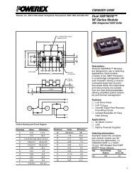
<strong>CM900DUC</strong>-<strong>24NF</strong><br />
<strong>Mega</strong> <strong>Power</strong> <strong>Dual</strong> IGBTMOD<br />
900 Amperes/1200 Volts<br />
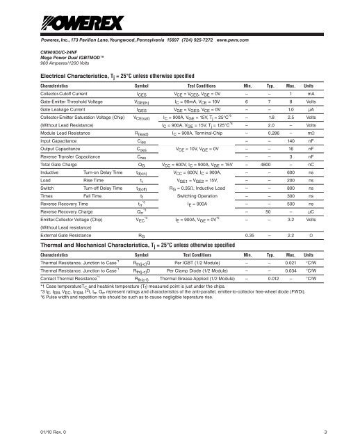
Electrical Characteristics, T j = 25°C unless otherwise specified<br />
Characteristics Symbol Test Conditions Min. Typ. Max. Units<br />
Collector-Cutoff Current I CES V CE = V CES , V GE = 0V – – 1 mA<br />
Gate-Emitter Threshold Voltage V GE(th) I C = 90mA, V CE = 10V 6 7 8 Volts<br />
Gate Leakage Current I GES V GE = V GES , V CE = 0V – – 1.0 µA<br />
Collector-Emitter Saturation Voltage (Chip) V CE(sat) I C = 900A, V GE = 15V, T j = 25°C *6 – 1.8 2.5 Volts<br />
(Without Lead Resistance) I C = 900A, V GE = 15V, T j = 125°C *6 – 2.0 – Volts<br />
Module Lead Resistance R (lead) I C = 900A, Terminal-Chip – 0.286 – mΩ<br />
Input Capacitance C ies – – 140 nF<br />
Output Capacitance C oes V CE = 10V, V GE = 0V – – 16 nF<br />
Reverse Transfer Capacitance C res – – 3 nF<br />
Total Gate Charge Q G V CC = 600V, I C = 900A, V GE = 15V – 4800 – nC<br />
Inductive Turn-on Delay Time t d(on) V CC = 600V, I C = 900A, – – 600 ns<br />
Load Rise Time t r V GE1 = V GE2 = 15V, – – 200 ns<br />
Switch Turn-off Delay Time t d(off) R G = 0.35Ω, Inductive Load – – 800 ns<br />
Times Fall Time t f Switching Operation – – 300 ns<br />
Reverse Recovery Time t rr<br />
*3<br />
Reverse Recovery Charge Q rr<br />
*3<br />
Emitter-Collector Voltage (Chip) V EC<br />
*3<br />
(Without Lead resistance)<br />
I E = 900A – – 500 ns<br />
– 50 – µC<br />
I E = 900A, V GE = 0V *6 – – 3.2 Volts<br />
External Gate Resistance R G 0.35 – 2.2 Ω<br />
Thermal and Mechanical Characteristics, T j = 25°C unless otherwise specified<br />
Characteristics Symbol Test Conditions Min. Typ. Max. Units<br />
Thermal Resistance, Junction to Case *1 R th(j-c) Q Per IGBT (1/2 Module) – – 0.021 °C/W<br />
Thermal Resistance, Junction to Case *1 R th(j-c) D Per Clamp Diode (1/2 Module) – – 0.034 °C/W<br />
Contact Thermal Resistance *1 R th(c-f) Thermal Grease Applied (1/2 Module) – 0.012 – °C/W<br />
*1 Case temperatureT C and heatsink temperature (T f ) measured point is just under the chips.<br />
*3 I E , I EM , V EC , I FSM , I 2 t, t rr , Q rr represent ratings and characteristics of the anti-parallel, emitter-to-collector free-wheel diode (FWDi).<br />
*6 Pulse width and repetition rate should be such as to cause negligible teperature rise.<br />
01/10 Rev. 0<br />
3