TxRx Designing tunable resonators and filters with constant bandwidth
TxRx Designing tunable resonators and filters with constant bandwidth
TxRx Designing tunable resonators and filters with constant bandwidth

Create successful ePaper yourself
Turn your PDF publications into a flip-book with our unique Google optimized e-Paper software.
<strong>TxRx</strong><br />
<strong>Designing</strong> <strong>tunable</strong><br />
<strong>resonators</strong> <strong>and</strong><br />
<strong>filters</strong> <strong>with</strong> <strong>constant</strong><br />
b<strong>and</strong>width<br />
Implementing step-impedance planar<br />
structures to increase performance in<br />
L- <strong>and</strong> T- types of coupling sections.<br />
By Boris Kapilevich<br />
<strong>and</strong> Roman Lukjanets<br />
As the number of wireless communications<br />
devices continues to increase logarithmically, a<br />
natural by-product is a crowded spectrum. One<br />
method of addressing this crowded spectrum integrates<br />
<strong>tunable</strong> <strong>filters</strong> in systems.<br />
<strong>with</strong> L <strong>and</strong> T - coupling sections. It will also introduce<br />
an active device for loss compensation.<br />
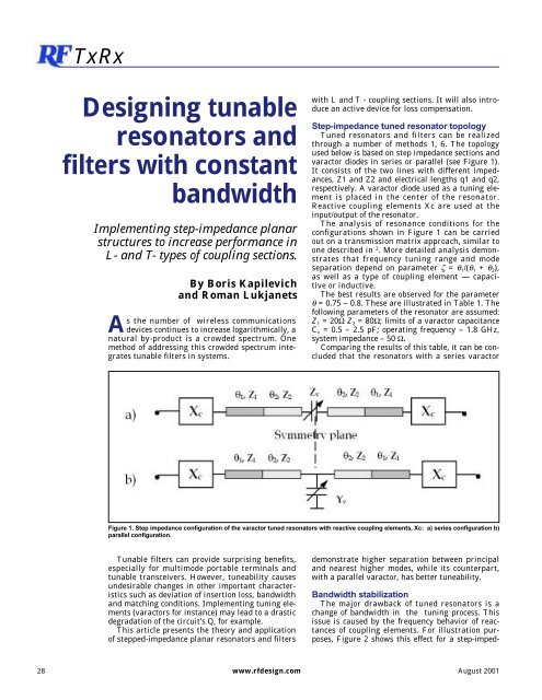
Step-impedance tuned resonator topology<br />
Tuned <strong>resonators</strong> <strong>and</strong> <strong>filters</strong> can be realized<br />
through a number of methods 1, 6. The topology<br />
used below is based on step impedance sections <strong>and</strong><br />
varactor diodes in series or parallel (see Figure 1).<br />
It consists of the two lines <strong>with</strong> different impedances,<br />
Z1 <strong>and</strong> Z2 <strong>and</strong> electrical lengths q1 <strong>and</strong> q2,<br />
respectively. A varactor diode used as a tuning element<br />
is placed in the center of the resonator.<br />
Reactive coupling elements Xc are used at the<br />
input/output of the resonator.<br />
The analysis of resonance conditions for the<br />
configurations shown in Figure 1 can be carried<br />
out on a transmission matrix approach, similar to<br />
one described in 2 . More detailed analysis demonstrates<br />
that frequency tuning range <strong>and</strong> mode<br />
separation depend on parameter ζ = θ 1 /(θ 1 + θ 2 ),<br />
as well as a type of coupling element — capacitive<br />
or inductive.<br />
The best results are observed for the parameter<br />
θ = 0.75 – 0.8. These are illustrated in Table 1. The<br />
following parameters of the resonator are assumed:<br />
Z 1 = 20Ω Z 2 = 80Ω; limits of a varactor capacitance<br />
C v = 0.5 – 2.5 pF; operating frequency – 1.8 GHz,<br />
system impedance – 50 Ω.<br />
Comparing the results of this table, it can be concluded<br />
that the <strong>resonators</strong> <strong>with</strong> a series varactor<br />
Figure 1. Step impedance configuration of the varactor tuned <strong>resonators</strong> <strong>with</strong> reactive coupling elements, Xc: a) series configuration b)<br />
parallel configuration.<br />
Tunable <strong>filters</strong> can provide surprising benefits,<br />
especially for multimode portable terminals <strong>and</strong><br />
<strong>tunable</strong> transceivers. However, tuneability causes<br />
undesirable changes in other important characteristics<br />
such as deviation of insertion loss, b<strong>and</strong>width<br />
<strong>and</strong> matching conditions. Implementing tuning elements<br />
(varactors for instance) may lead to a drastic<br />
degradation of the circuit’s Q, for example.<br />
This article presents the theory <strong>and</strong> application<br />
of stepped-impedance planar <strong>resonators</strong> <strong>and</strong> <strong>filters</strong><br />
demonstrate higher separation between principal<br />
<strong>and</strong> nearest higher modes, while its counterpart,<br />
<strong>with</strong> a parallel varactor, has better tuneability.<br />
B<strong>and</strong>width stabilization<br />
The major drawback of tuned <strong>resonators</strong> is a<br />
change of b<strong>and</strong>width in the tuning process. This<br />
issue is caused by the frequency behavior of reactances<br />
of coupling elements. For illustration purposes,<br />
Figure 2 shows this effect for a step-imped-<br />
28 www.rfdesign.com August 2001
Table 1. Comparison of step-impedance resonator characteristics.<br />
ance resonator <strong>with</strong> a varactor in<br />
series. An approximated a 50% widening<br />
in b<strong>and</strong>width has taken place from<br />
20 MHz to 32 MHz.<br />
The following resonator parameters<br />
are assumed: Z 1 = 20Ω; Z 2 = 80Ω; limits<br />
of a varactor capacitance C v = 0.5 – 2.5<br />
pF; operating frequency – 1.5 GHz; system<br />
impedance – 50Ω; coupling capacitor<br />
– 0.5 pF. The resonator is designed<br />
on the basis of microstrip line <strong>with</strong> substrate<br />
ε r = 2.6, h = 2 mm, <strong>and</strong> loss tangent<br />
tgδ = 0.001.<br />
The first step in stabilizing b<strong>and</strong>width<br />
uses proper reactive coupling<br />
elements to compensate for b<strong>and</strong>width<br />
change. One such element is the L-section<br />
3 . Among eight available configurations,<br />
the capacitor-based L-section is<br />
preferable when taking into account<br />
fabricating facilities. Table 2 <strong>and</strong><br />
Figure 3 present the effects of b<strong>and</strong>width<br />
stabilization when L-type coupling<br />
elements are used instead of a<br />
single capacitor. B<strong>and</strong>width stabilizing<br />
factor is about 50.<br />
To verify the b<strong>and</strong>width stabilization<br />
effect, the experimental version of the<br />
step-impedance resonator was fabricated<br />
<strong>with</strong> specifications shown in Table 3.<br />
Figure 2. Illustration of changing b<strong>and</strong>width in a tuning process.<br />
30 www.rfdesign.com August 2001
Table 2. Changing b<strong>and</strong>width comparison.<br />
The comparison of the calculated <strong>and</strong><br />
measured transmission coefficients, S 21 ,<br />
are presented in Figure 4. Taking into<br />
account the biasing circuit, an agreement<br />
between calculated <strong>and</strong> measured<br />
data is observed.<br />
B<strong>and</strong>width stabilization <strong>with</strong> L-type<br />
capacitor coupling elements at<br />
input/output of the step impedance<br />
resonator.<br />
Figure 3. B<strong>and</strong>width stabilization <strong>with</strong> L-type capacitor coupling elements at input/output of the stepimpedance<br />
resonator.<br />
Passively coupled <strong>resonators</strong><br />
The same approach can be applied to<br />
the design of passively coupled tuned<br />
<strong>resonators</strong> <strong>with</strong> <strong>constant</strong> b<strong>and</strong>width. In<br />
this case, choose both the external <strong>and</strong><br />
internal coupling elements to compensate<br />
for a change of coupling coefficients<br />
in the process of tuning. Figure 5<br />
demonstrates the transformation of a<br />
single resonator to its coupled counterpart<br />
based on capacitive L-type sections.<br />
As a result, the coupling element<br />
between <strong>resonators</strong> can be formed using<br />
a T-type capacitive section. The configuration<br />
of a tuned step-impedance filter of<br />
the second order is shown in Figure 6.<br />
Optimization, based on the simplex<br />
search technique, finds a specification<br />
of the T-section providing <strong>constant</strong><br />
b<strong>and</strong>width of the second-order tuned<br />
filter. Table 4 demonstrates characteristics<br />
of such a filter before <strong>and</strong> after<br />
internal coupling elements are optimized.<br />
The frequency response of the<br />
tuned second-order filter is shown in<br />
Figure 7. The b<strong>and</strong>width stabilization<br />
factor is 12, but the insertion loss has<br />
increased to 10 dB. Thus, a measurement<br />
must be undertaken for loss<br />
compensation.<br />
An experiment was carried out <strong>with</strong><br />
the microstrip second-order tuned filter.<br />
Its specifications are given in Table<br />
5. A comparison of calculated <strong>and</strong> measured<br />
filter performance is depicted in<br />
Figure 8, which takes biasing circuits<br />
into account.<br />
Active tuned filter<br />
Having chosen the topology of uncoupled<br />
<strong>and</strong> coupled tuned <strong>resonators</strong> <strong>with</strong><br />
near-<strong>constant</strong> b<strong>and</strong>width, a proper filter<br />
of higher order can be built up.<br />
However, insertion losses are increased<br />
drastically. As a result, special measures<br />
for their compensation must be<br />
suggested in a practice.<br />
One way to do this is to transform a<br />
passive tuned filter to its active counterpart<br />
by adding an active device. A<br />
variety of microwave active filter configurations<br />
are available for practice 4 .<br />
Recently, an idea based on actively coupled<br />
<strong>resonators</strong> was presented 5 . Such<br />
<strong>resonators</strong> are almost non-interactive<br />
because of the use of a transistor as a<br />
coupling element between <strong>resonators</strong>.<br />
Therefore, the circuit sensitivity to fabricating<br />
tolerances is reduced by applying<br />
them in a cascade arrangement.<br />
Different combinations of <strong>resonators</strong><br />
can then be applied to achieve the<br />
desired filter characteristic. The two<br />
passively coupled <strong>resonators</strong> are actively<br />
coupled in a cascade configuration<br />
shown in Figure 9 to form the equivalent<br />
active filter of the fourth order.<br />
The b<strong>and</strong>width is almost <strong>constant</strong>, but<br />
insertion loss is increased about 5 dB<br />
when the filter is tuned toward higher<br />
frequencies. Therefore, an active device<br />
must provide a gain of 9 dB at low, <strong>and</strong><br />
14 dB at high frequencies of the tuning<br />
32 www.rfdesign.com August 2001
tuned. This drawback can be eliminated<br />
by more careful design of the matching<br />
elements of the active device.<br />
Figure 4. Calculated <strong>and</strong> measured results for the step impedance resonator. Tuning range: 48%; insertion<br />
losses 4 to 6 dB; b<strong>and</strong>width: 50 MHz at 3dB level; minimum separation between principal <strong>and</strong> nearest<br />
higher mode: 1010 MHz; b<strong>and</strong>width changing: 2.3%<br />
Conclusion<br />
When designing <strong>tunable</strong> <strong>resonators</strong><br />
<strong>and</strong> <strong>filters</strong> <strong>with</strong> <strong>constant</strong> b<strong>and</strong>width,<br />
implement L-<strong>and</strong> T-types of coupling<br />
elements to achieve the stabilization of<br />
b<strong>and</strong>width in the tuning process. An<br />
active device <strong>with</strong> predicted slope of<br />
the gain can be used for a loss compensation.<br />
The final active filter layout<br />
<strong>and</strong> performance has been verified in<br />
experiments carried out <strong>with</strong> fourthorder<br />
filter in a cascade configuration.<br />
range for a loss compensation <strong>and</strong><br />
amplitude equalization. The above<br />
requirement has been realized using<br />
commercial, off-the-shelf (COTS) transistors.<br />
The matching elements of the<br />
amplifier have been designed to provide<br />
the required slope of the gain.<br />
The active filter consists of two Al 2 O 3<br />
substrates 48 x 60 mm 2 , having h = 1<br />
Table 3. The characteristics of an experimental step-impedance resonator.<br />
Figure 5. Transformation of L-type section of uncoupled resonator into T-section of coupled counterpart.<br />
Figure 6. Configuration of the tuned step-impedance 2 nd order filter.<br />
Acknowledgment<br />
This work has been supported by EC<br />
INTAS Project 96-0851, <strong>and</strong> the<br />
authors would like to thank the project<br />
coordinators Prof. B. Jarry (I.R.C.O.M.,<br />
France) <strong>and</strong> Prof. M.Guflielmi (ESA<br />
ESTEC, The Netherl<strong>and</strong>s) for their<br />
useful advice <strong>and</strong> discussions of some<br />
problems associated <strong>with</strong> the topics<br />
considered, as well as engineer V.<br />
Smirnoff (SibSUTI, Russia) for his help<br />
in experiments.<br />
References<br />
[1] F.E. Van Vliet, “Modern Very<br />
Narrow B<strong>and</strong> MMIC Filters <strong>and</strong> Tuning<br />
Methods”, Paris EuMW’2000 -<br />
Workshop (WS8) - “New Techniques<br />
<strong>and</strong> New Technologies for RF <strong>and</strong><br />
Microwave Filters”<br />
mm, ε r = 9.6. Each is used for arranging<br />
passively coupled <strong>resonators</strong> <strong>and</strong><br />
matching circuits of the active device<br />
on its input <strong>and</strong> output. The active<br />
device is placed between them. Figure<br />
10 demonstrates the final performance<br />
of the active tuned filter of the fourth<br />
order <strong>with</strong> the <strong>constant</strong> b<strong>and</strong>width.<br />
By implementing an active device,<br />
the full compensation of the insertion<br />
loss is achieved. However, the change of<br />
return loss takes place when the filter is<br />
Table 4. The coupled resonator components before <strong>and</strong> after optimization.<br />
34 www.rfdesign.com August 2001
Figure 7. The frequency response of the tuned step-impedance filter of the second order <strong>with</strong> near-<strong>constant</strong><br />
b<strong>and</strong>width.<br />
[2] B.Kapilevich, R.Lukyanets, “B.<br />
Kapilevich, R.Lukyanets, “Modeling<br />
Varactor Tunable Microstrip Resonators<br />
for Wireless Applications,”<br />
Applied Microwave & Wireless, Vol.10,<br />
no.7, September 1998, pp.32 - 44; Vol.<br />
13, no. 5, May 2001, pp. 54-64.<br />
[3] P.H.Smith, “Electronic Applications<br />
of the Smith Chart in Waveguide,<br />
Circuits <strong>and</strong> Component Analysis”,<br />
McGraw Hill Book Co., 1969.<br />
[4] B. Kapilevich, “Microwave Active<br />
Filters for Wireless Applications”, Paris<br />
EuMW’2000 - Workshop (WS8) - “New<br />
Techniques <strong>and</strong> New Technologies for<br />
RF <strong>and</strong> Microwave Filters.”<br />
[5] F. Sabouri-S, C.Christensen,<br />
T.Larsen, “A Single-Chip GaAs MMIC<br />
Image-Rejection Front-End for Digital<br />
European Cordless Telecommunications”,<br />
IEEE Trans. on MTT, vol.48,<br />
no.8, August, 2000, pp.1318 - 1325.<br />
[6] K. Jeganathan, “Design of Simple<br />
Tunable/Switchable B<strong>and</strong>pass Filter”<br />
Applied Microwave & Wireless, March<br />
2000, pp.32 - 40.<br />
36 www.rfdesign.com August 2001
Table 5. The specifications of microstrip second-order filter.<br />
Figure 8. Calculated <strong>and</strong> measured results for the step-impedance coupled resonator: Tuning range:<br />
33%; insertion losses: 7 to 8 dB; b<strong>and</strong>width: 30 MHz at 3 dB level; minimum separation between principal<br />
<strong>and</strong> nearest higher mode: 695 MHz; b<strong>and</strong>width changing; 3%.<br />
Figure 9. Configuration of actively coupled <strong>resonators</strong> forming the equivalent active filter of fourth<br />
order.<br />
About the authors<br />
Boris Kapilevich is a professor at<br />
Siberia State University of<br />
Telecommunication & Informatics,<br />
Novosibirsk, Russia. He received his<br />
M.S. degree from Tomsk State<br />
University in 1961, a Ph.D. in 1969<br />
from Novosibirsk State Technical<br />
University <strong>and</strong> a Dr.Sc.(technol.) in<br />
1986 from Moscow Power Energy<br />
University. He has more than 30<br />
years of experience in analysis <strong>and</strong><br />
design of various microwave/RF<br />
components <strong>and</strong> devices for the communications<br />
industry. His teaching<br />
<strong>and</strong> research interests are in areas<br />
of microwave <strong>and</strong> RF components for<br />
mobile <strong>and</strong> space communications.<br />
He can be reached at his office by<br />
tel.: +007-3832-660943, by fax: +007-<br />
3832-222581 or by e-mail:<br />
boris@neic.nsk.su .<br />
Roman Lukjanets is a Ph.D. student<br />
at Siberia State University of<br />
Telecommunication & Informatics,<br />
Novosibirsk, Russia. He received his<br />
M.S. degree from Siberia State<br />
University of Telecommunication &<br />
Informatics in 1996. His research<br />
interests are focused in microwave<br />
<strong>and</strong> RF components for mobile communications,<br />
including microwave<br />
active filter. Contact the authors at:<br />
Siberia State University of<br />
Telecommunications <strong>and</strong> Informatics<br />
86 Kirova str., Novosibirsk, Russia –<br />
630102.<br />
Figure 10. The calculated performance of passively coupled <strong>resonators</strong> shown in Figure 9.<br />
38 www.rfdesign.com August 2001